TSL251中文资料
- 格式:pdf
- 大小:150.91 KB
- 文档页数:7
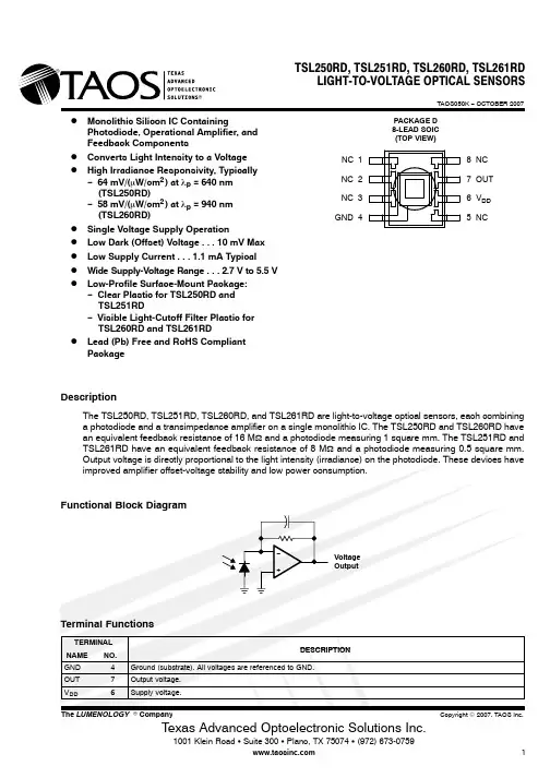
D Monolithic Silicon IC Containing Photodiode, Operational Amplifier, and Feedback ComponentsD Converts Light Intensity to a Voltage DHigh Irradiance Responsivity, Typically − 64 mV/(m W/cm 2) at l p = 640 nm (TSL250RD)− 58 mV/(m W/cm 2) at l p = 940 nm (TSL260RD)D Single Voltage Supply OperationD Low Dark (Offset) Voltage ...10 mV Max D Low Supply Current ...1.1 mA TypicalD Wide Supply-Voltage Range ...2.7 V to 5.5 V DLow-Profile Surface-Mount Package:− Clear Plastic for TSL250RD and TSL251RD− Visible Light-Cutoff Filter Plastic for TSL260RD and TSL261RDDLead (Pb) Free and RoHS Compliant PackageDescriptionThe TSL250RD, TSL251RD, TSL260RD, and TSL261RD are light-to-voltage optical sensors, each combining a photodiode and a transimpedance amplifier on a single monolithic IC. The TSL250RD and TSL260RD have an equivalent feedback resistance of 16 M Ω and a photodiode measuring 1 square mm. The TSL251RD and TSL261RD have an equivalent feedback resistance of 8 M Ω and a photodiode measuring 0.5 square mm.8 NC 7 OUT 6 V DD 5 NCPACKAGE D 8-LEAD SOIC (TOP VIEW)NC 1NC 2NC 3GND 4TSL250RD, TSL251RD, TSL260RD, TSL261RD LIGHT-TO-VOLTAGE OPTICAL SENSORSAbsolute Maximum Ratings over operating free-air temperature range (unless otherwise noted)†Supply voltage, V DD (see Note 1) 6 V . . . . . . . . . . . . . . . . . . . . . . . . . . . . . . . . . . . . . . . . . . . . . . . . . . . . . . . . . . . . . Output current, I O ±10 mA . . . . . . . . . . . . . . . . . . . . . . . . . . . . . . . . . . . . . . . . . . . . . . . . . . . . . . . . . . . . . . . . . . . . . . Duration of short-circuit current at (or below) 25°C (see Note 2) 5 s . . . . . . . . . . . . . . . . . . . . . . . . . . . . . . . . . . . Operating free-air temperature range, T A −25°C to 85°C . . . . . . . . . . . . . . . . . . . . . . . . . . . . . . . . . . . . . . . . . . . . Storage temperature range, T stg −25°C to 85°C . . . . . . . . . . . . . . . . . . . . . . . . . . . . . . . . . . . . . . . . . . . . . . . . . . . . Solder conditions in accordance with JEDEC J −STD −020A, maximum temperature (see Note 3) 260°C. . . †Stresses beyond those listed under “absolute maximum ratings” may cause permanent damage to the device. These are stress ratings only, and functional operation of the device at these or any other conditions beyond those indicated under “recommended operating conditions” is not implied. Exposure to absolute-maximum-rated conditions for extended periods may affect device reliability.NOTES: 1.All voltages are with respect to GND.2.Output may be shorted to supply.3.The device may be hand soldered provided that heat is applied only to the solder pad and no contact is made between the tip ofthe solder iron and the device lead. The maximum time heat should be applied to the device is 5 seconds.Recommended Operating ConditionsMINNOMMAX UNIT Supply voltage, V DD2.7 5.5V Operating free-air temperature, T A70°CElectrical Characteristics at V DD = 5 V, T A = 25°C, R L = 10 k Ω (unless otherwise noted) (see Notes 3, 4, 5, and 6)Sλp = 640 nmλp = 940 nmTEST CONDITIONS TSL250RD TSL251RDTSL260RDTSL261RDPARAMETERMIN TYP MAX MIN TYP MAX MIN TYP MAX MIN TYP MAX UNITV D Dark voltage E e = 00510051005100510mV V OMMaximum output voltageV DD = 4.5 V 3 3.333.333.333.3V E e = 31 μW/cm 21.522.5Output E e = 124 μW/cm 2 1.522.5V OvoltageE e = 34 μW/cm 2123VE e = 132 μW/cm 2123R eIrradiance responsivitySee Note 764165815mV/(μW/cm 2)Temperature V O = 2 V @ 25°C, 0°C to 702288mV/°C coefficient ofoutput voltage (V O )T A = 0°C (see Note 8)0.10.10.40.4%/°C E e = 31 μW/cm 21.11.7Supply E e = 124 μW/cm 2 1.11.7I DDcurrentE e = 34 μW/cm 2 1.11.7mAE e = 132 μW/cm 21.11.7NOTES: 4.Measurements are made with R L = 10 k Ω between output and ground.5.Optical measurements are made using small-angle incident radiation from an LED optical source.6.The 640 nm input irradiance E e is supplied by an Al I nGaP LED with peak wavelength λp = 640 nm.7.The 940 nm input irradiance E e is supplied by a GaAs LED with peak wavelength λp = 940 nm.8.Irradiance responsivity is characterized over the range V O = V D to 3 V. The best-fit straight line of Output Voltage V O versus irradiance E e over this range will typically have a positive extrapolated V O value for E e = 0.9.The temperature coefficient of output voltage measurement is made by adjusting irradiance such that V O is approximately 2 V at25°C and then with irradiance held constant, measuring V O while varying the temperature between 0°C and 70°C.TSL250RD, TSL251RD, TSL260RD, TSL261RDLIGHT-TO-VOLTAGE OPTICAL SENSORSTAOS050K − OCTOBER 2007Dynamic Characteristics at V DD = 5 V , T A = 25°C, R L = 10 k Ω (unless otherwise noted) (see Figure 1)Sλp = 640 nmλp = 940 nmTEST TSL250RD TSL251RDTSL260RDTSL261RDPARAMETERCONDITIONSMINTYP MAXMINTYP MAXMINTYP MAXMINTYP MAXUNITt r Output pulse rise time V O(peak) = 2 V2607026070μs tf Output pulse fall time VO(peak) = 2 V 2607026070μsV nOutput noise voltageE e = 0, f = 1000 Hz0.80.70.80.7μV/(√(Hz))VOLTAGE WAVEFORMTEST CIRCUITOutput (see Note B)V OutputfNOTES: A.The input irradiance is supplied by a pulsed light-emitting diode with t r < 1 μs, t f < 1 μs.B.The output waveform is monitored on an oscilloscope with the following characteristics: t r < 100 ns, Z i ≥ 1 M Ω, C i ≤ 20 pF.Figure 1. Switching TimesTSL250RD, TSL251RD, TSL260RD, TSL261RD LIGHT-TO-VOLTAGE OPTICAL SENSORSTAOS050K − OCTOBER 2007TYPICAL CHARACTERISTICSOUTPUT VOLTAGEvsIRRADIANCEFigure 20.11101001000O u t p u t V o l t a g e (V O − V D ) — VE e — Irradiance — m W/cm 20.010.1110OUTPUT VOLTAGEvsIRRADIANCEFigure 30.11101001000E e — Irradiance — m W/cm 20.010.1110O u t p u t V o l t a g e (V O − V D ) —VFigure 430040050060070010008009001100λ − Wavelength − nmR e l a t i v e R e s p o n s i v i t y00.20.40.60.81.01.2PHOTODIODE SPECTRAL RESPONSIVITYFigure 5PHOTODIODE SPECTRAL RESPONSIVITYλ − Wavelength − nm7008009001000110060000.20.40.60.81R e l a t i v e R e s p o n s i v i t yTSL250RD, TSL251RD, TSL260RD, TSL261RDLIGHT-TO-VOLTAGE OPTICAL SENSORSTAOS050K − OCTOBER 2007TYPICAL CHARACTERISTICSFigure 6MAXIMUM OUTPUT VOLTAGEvsSUPPLY VOLTAGEV DD − Supply Voltage − V0123452.533.544.555.5V O M — Ma x i m u m O u t p u t V o l t a g e — VFigure 701234V O − Output Voltage − VSUPPLY CURRENTvsOUTPUT VOLTAGEI D D — S u p p l y C u r r e n t — m A0.40.60.811.21.4Figure 8NORMALIZED OUTPUT VOLTAGEvs.ANGULAR DISPLACEMENTQ − Angular Displacement − °V O — O ut p u t V o l t a g e — N o r m a l i z e d00.20.40.60.81−90−60−300306090TSL250RD, TSL251RD, TSL260RD, TSL261RD LIGHT-TO-VOLTAGE OPTICAL SENSORSTAOS050K − OCTOBER 2007APPLICATION INFORMATIONPower Supply ConsiderationsFor optimum device performance, power-supply lines should be decoupled by a 0.01-μF to 0.1-μF capacitor with short leads connected between VDD and GND mounted close to the device package.Device Operational DetailsThe voltage developed at the output pin (OUT) is given by:V O = V D + (R e ) (E e )where:V O is the output voltageV D is the output voltage for dark condition (E e = 0)R e is the device responsivity for a given wavelength of light given in mV/(μW/cm 2)E eis the incident irradiance in μW/cm 2V D is a fixed offset voltage resulting primarily from the input offset voltage of the internal op amp. As shown in the equation above, this voltage represents a constant, light-independent term in the total output voltage V O .At low light levels, this offset voltage can be a significant percentage of V O . For optimum performance of any given device over the full output range, the value of V D should be measured (in the absence of light) and later subtracted from all subsequent light measurements (see Figures 2 and 3).PCB Pad LayoutSuggested PCB pad layout guidelines for the D package is shown in Figure 9.NOTES: A.All linear dimensions are in millimeters.B.This drawing is subject to change without notice.Figure 9. Suggested D Package PCB LayoutTSL250RD, TSL251RD, TSL260RD, TSL261RDLIGHT-TO-VOLTAGE OPTICAL SENSORSTAOS050K − OCTOBER 2007MECHANICAL DATAThis SOIC package consists of an integrated circuit mounted on a lead frame and encapsulated with an electrically nonconductive clear plastic compound. The photodiode area is typically 1.02 mm 2 for the TSL250RD and TSL260RD,and is typically 0.514 mm 2 for the TSL251RD and TSL261RD.PACKAGE DPLASTIC SMALL-OUTLINENOTES: A.All linear dimensions are in millimeters.B.The center of the photo-active area is referenced to the upper left corner tip of the lead frame (Pin 1).C.Package is molded with an electrically nonconductive clear plastic compound having an index of refraction of 1.55.D.This drawing is subject to change without notice.Figure 10. Package D — Plastic Small Outline IC Packaging ConfigurationTSL250RD, TSL251RD, TSL260RD, TSL261RD LIGHT-TO-VOLTAGE OPTICAL SENSORSTAOS050K − OCTOBER 2007MECHANICAL DATASIDE VIEWDETAIL B6.45 + 0.10[0.254 + 0.004]5.13 + 0.10[0.202 + 0.004]DETAIL A NOTES: A.All linear dimensions are in millimeters [inches].B.The dimensions on this drawing are for illustrative purposes only. Dimensions of an actual carrier may vary slightly.C.Symbols on drawing A o , B o , and K o are defined in ANSI EIA Standard 481−B 2001.D.Each reel is 178 millimeters in diameter and contains 1000 parts.E.TAOS packaging tape and reel conform to the requirements of EIA Standard 481−B.F.This drawing is subject to change without notice.Figure 11. Package D Carrier TapeTSL250RD, TSL251RD, TSL260RD, TSL261RDLIGHT-TO-VOLTAGE OPTICAL SENSORSTAOS050K − OCTOBER 2007MANUFACTURING INFORMATIONThe Plastic Small Outline IC package (D) has been tested and has demonstrated an ability to be reflow soldered to a PCB substrate.The solder reflow profile describes the expected maximum heat exposure of components during the solder reflow process of product on a PCB. Temperature is measured on top of component. The component should be limited to a maximum of three passes through this solder reflow profile.Table 1. TSL2xxRD Solder Reflow ProfilePARAMETERREFERENCETSL2xxRD Average temperature gradient in preheating 2.5°C/sec Soak time t soak 2 to 3 minutes Time above 217°C t 1Max 60 sec Time above 230°C t 2Max 50 sec Time above T peak −10°C t 3Max 10 sec Peak temperature in reflow T peak 260° C (−0°C/+5°C)Temperature gradient in coolingMax −5°C/secT Figure 12. TSL2xxRD Solder Reflow Profile GraphTSL250RD, TSL251RD, TSL260RD, TSL261RD LIGHT-TO-VOLTAGE OPTICAL SENSORSTAOS050K − OCTOBER 2007Moisture SensitivityOptical characteristics of the device can be adversely affected during the soldering process by the release and vaporization of moisture that has been previously absorbed into the package molding compound. To prevent these adverse conditions, all devices shipped in carrier tape have been pre-baked and shipped in a sealed moisture-barrier bag. No further action is necessary if these devices are processed through solder reflow within 24 hours of the seal being broken on the moisture-barrier bag.However, for all devices shipped in tubes or if the seal on the moisture barrier bag has been broken for 24 hours or longer, it is recommended that the following procedures be used to ensure the package molding compound contains the smallest amount of absorbed moisture possible.For devices shipped in tubes:1.Remove devices from tubes2.Bake devices for 4 hours, at 90°C3.After cooling, load devices back into tubes4.Perform solder reflow within 24 hours after bakeBake only a quantity of devices that can be processed through solder reflow in 24 hours. Devices can be re-baked for 4 hours, at 90°C for a cumulative total of 12 hours (3 bakes for 4 hours at 90°C).For devices shipped in carrier tape:1.Bake devices for 4 hours, at 90°C in the tape2.Perform solder reflow within 24 hours after bakeBake only a quantity of devices that can be processed through solder reflow in 24 hours. Devices can be re −baked for 4 hours in tape, at 90°C for a cumulative total of 12 hours (3 bakes for 4 hours at 90°C).TSL250RD, TSL251RD, TSL260RD, TSL261RD LIGHT-TO-VOLTAGE OPTICAL SENSORSTAOS050K − OCTOBER 2007PRODUCTION DATA — information in this document is current at publication date. Products conform to specifications in accordance with the terms of Texas Advanced Optoelectronic Solutions, Inc. standard warranty. Production processing does not necessarily include testing of all parameters.LEAD-FREE (Pb-FREE) and GREEN STATEMENTPb-Free (RoHS) TAOS’ terms Lead-Free or Pb-Free mean semiconductor products that are compatible with the current RoHS requirements for all 6 substances, including the requirement that lead not exceed 0.1% by weight in homogeneous materials. Where designed to be soldered at high temperatures, TAOS Pb-Free products are suitable for use in specified lead-free processes.Green (RoHS & no Sb/Br) TAOS defines Green to mean Pb-Free (RoHS compatible), and free of Bromine (Br) and Antimony (Sb) based flame retardants (Br or Sb do not exceed 0.1% by weight in homogeneous material).Important Information and Disclaimer The information provided in this statement represents TAOS’ knowledge and belief as of the date that it is provided. TAOS bases its knowledge and belief on information provided by third parties,and makes no representation or warranty as to the accuracy of such information. Efforts are underway to better integrate information from third parties. TAOS has taken and continues to take reasonable steps to provide representative and accurate information but may not have conducted destructive testing or chemical analysis on incoming materials and chemicals. TAOS and TAOS suppliers consider certain information to be proprietary, and thus CAS numbers and other limited information may not be available for release.NOTICETexas Advanced Optoelectronic Solutions, Inc. (TAOS) reserves the right to make changes to the products contained in this document to improve performance or for any other purpose, or to discontinue them without notice. Customers are advised to contact TAOS to obtain the latest product information before placing orders or designing TAOS products into systems.TAOS assumes no responsibility for the use of any products or circuits described in this document or customer product design, conveys no license, either expressed or implied, under any patent or other right, and makes no representation that the circuits are free of patent infringement. TAOS further makes no claim as to the suitability of its products for any particular purpose, nor does TAOS assume any liability arising out of the use of any product or circuit, and specifically disclaims any and all liability, including without limitation consequential or incidental damages.TEXAS ADVANCED OPTOELECTRONIC SOLUTIONS, INC. PRODUCTS ARE NOT DESIGNED OR INTENDED FOR USE IN CRITICAL APPLICATIONS IN WHICH THE FAILURE OR MALFUNCTION OF THE TAOS PRODUCT MAY RESULT IN PERSONAL INJURY OR DEATH. USE OF TAOS PRODUCTS IN LIFE SUPPORT SYSTEMS IS EXPRESSLY UNAUTHORIZED AND ANY SUCH USE BY A CUSTOMER IS COMPLETELY AT THE CUSTOMER’S RISK.LUMENOLOGY, TAOS, the TAOS logo, and Texas Advanced Optoelectronic Solutions are registered trademarks of Texas Advanced Optoelectronic Solutions Incorporated.TSL250RD, TSL251RD, TSL260RD, TSL261RD LIGHT-TO-VOLTAGE OPTICAL SENSORSTAOS050K − OCTOBER 2007。
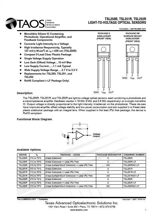
D Monolithic Silicon IC Containing Photodiode, Operational Amplifier, and Feedback ComponentsD Converts Light Intensity to a Voltage D High Irradiance Responsivity, Typically 137 mV/(m W/cm 2) at l p = 635 nm (TSL250R)D Compact 3-Lead Clear Plastic Package D Single Voltage Supply OperationD Low Dark (Offset) Voltage....10 mV Max D Low Supply Current......1.1 mA TypicalD Wide Supply-Voltage Range.... 2.7 V to 5.5 V D Replacements for TSL250, TSL251, and TSL252DRoHS Compliant (−LF Package Only)DescriptionThe TSL250R, TSL251R, and TSL252R are light-to-voltage optical sensors, each combining a photodiode and a transimpedance amplifier (feedback resistor = 16 M Ω, 8 M Ω, and 2.8 M Ω respectively) on a single monolithic IC. Output voltage is directly proportional to the light intensity (irradiance) on the photodiode. These devices have improved amplifier offset-voltage stability and low power consumption and are supplied in a 3-lead clear plastic sidelooker package with an integral lens. When supplied in the lead (Pb) free package, the device is RoHS compliant.Functional Block DiagramPACKAGE S SIDELOOKER (FRONT VIEW)1GND2V DD3OUTPACKAGE SM SURFACE MOUNT SIDELOOKER (FRONT VIEW)1GND2V DD3OUTTSL250R, TSL251R, TSL252RLIGHT-TO-VOLTAGE OPTICAL SENSORSTerminal FunctionsTERMINAL NAME NO.DESCRIPTIONGND 1Ground (substrate). All voltages are referenced to GND.OUT 3Output voltage V DD2Supply voltageAbsolute Maximum Ratings over operating free-air temperature range (unless otherwise noted)†Supply voltage, V DD (see Note 1) 6 V . . . . . . . . . . . . . . . . . . . . . . . . . . . . . . . . . . . . . . . . . . . . . . . . . . . . . . . . . . . . . Output current, I O ±10 mA . . . . . . . . . . . . . . . . . . . . . . . . . . . . . . . . . . . . . . . . . . . . . . . . . . . . . . . . . . . . . . . . . . . . . . Duration of short-circuit current at (or below) 25°C (see Note 2) 5 s . . . . . . . . . . . . . . . . . . . . . . . . . . . . . . . . . . . Operating free-air temperature range, T A −25°C to 85°C . . . . . . . . . . . . . . . . . . . . . . . . . . . . . . . . . . . . . . . . . . . . Storage temperature range, T stg −25°C to 85°C . . . . . . . . . . . . . . . . . . . . . . . . . . . . . . . . . . . . . . . . . . . . . . . . . . . . Lead temperature 1,6 mm (1/16 inch) from case for 10 seconds (S Package) 260°C . . . . . . . . . . . . . . . . . . . . Reflow solder, in accordance with J-STD-020C or J-STD-020D (SM Package) 260°C. . . . . . . . . . . . . . . . . . . †Stresses beyond those listed under “absolute maximum ratings” may cause permanent damage to the device. These are stress ratings only, and functional operation of the device at these or any other conditions beyond those indicated under “recommended operating conditions” is not implied. Exposure to absolute-maximum-rated conditions for extended periods may affect device reliability.NOTES: 1.All voltages are with respect to GND.2.Output may be shorted to supply.Recommended Operating ConditionsMINNOMMAX UNIT Supply voltage, V DD2.7 5.5V Operating free-air temperature, T A70°CTSL250R, TSL251R, TSL252RLIGHT-TO-VOLTAGE OPTICAL SENSORSTAOS028H − SEPTEMBER 2007Electrical Characteristics at V DD = 5 V , T A = 25°C, λp = 635 nm, R L = 10 k Ω (unless otherwise noted)(see Notes 3, 4, and 5)TEST TSL250R TSL251RTSL252RPARAMETER CONDITIONS MIN TYP MAX MIN TYP MAX MIN TYP MAX UNIT V D Dark voltage E e = 0041004100410mV V OMMaximum output voltage V DD = 4.5 V 3.0 3.3 3.03.33.03.3VE e = 14.6 μW/cm 21.522.5E e = 38.5 μW/cm 2 1.522.5V OOutput voltageE e = 196 μW/cm 2 1.522.5VE 2 1.6mV/°C Temperature e = 14.6 μW/cm ,T A = 0°C to 70°C 0.08%/°C E 2 1.6mV/°C αvocoefficient of output voltage )e = 38.5 μW/cm ,T A = 0°C to 70°C 0.08%/°C p g (V O E 2 1.6mV/°C e = 196 μW/cm ,T A = 0°C to 70°C 0.08%/°C Irradiance λp = 635 nm,See Notes 5 and 71375210.2N eresponsivityλp = 880 nm,See Notes 6 and 7127489.4mV/(μW/cm 2)E e = 14.6 μW/cm 21.11.7I Supply current E e = 38.5 μW/cm 2 1.11.7mADDpp yE e = 196 μW/cm 21.11.7NOTES: 3.Measurements are made with R L = 10 k Ω between output and ground.4.Optical measurements are made using small-angle incident radiation from an LED optical source.5.The input irradiance E e is supplied by an Al I nGaP LED with peak wavelength λp = 635 nm6.The input irradiance E e is supplied by a GaAlAs LED with peak wavelength λp = 880 nm7.Irradiance responsivity is characterized over the range V O = 0.05 to 2.9 V. The best-fit straight line of Output Voltage V O versus irradiance E e over this range will typically have a positive extrapolated V O value for E e = 0.Dynamic Characteristics at T A = 25°C (see Figure 1)TSL250R TSL251R TSL252R PARAMETERTEST CONDITIONS MINTYP MAXMINTYP MAXMINTYP MAXUNIT t r Output pulse rise time V DD = 5 V,λp = 635 nm 260707μs t f Output pulse fall time V DD = 5 V,λp = 635 nm 260707μs V nOutput noise voltageV DD = 5 V,f = 1000 HzE e = 0,0.80.70.6μV/√TSL250R, TSL251R, TSL252RLIGHT-TO-VOLTAGE OPTICAL SENSORSTAOS028H − SEPTEMBER 2007PARAMETER MEASUREMENT INFORMATIONVOLTAGE WAVEFORMTEST CIRCUITOutput (see Note B)OutputfNOTES: A.The input irradiance is supplied by a pulsed Al I nGaP light-emitting diode with the following characteristics: λp = 635 nm,t r < 1 μs, t f < 1 μs.B.The output waveform is monitored on an oscilloscope with the following characteristics: t r < 100 ns, Z i ≥ 1 M Ω, C i ≤20 pF.Figure 1. Switching Times0.4N o r m a l i z e d O u t p u t V o l t a g e 10.80.60.2θ − Angular Displacement80°60°40°20°0°80°60°40°20°NORMALIZED OUTPUT VOLTAGEvsANGULAR DISPLACEMENTV −OFigure 2TSL250R, TSL251R, TSL252RLIGHT-TO-VOLTAGE OPTICAL SENSORSTAOS028H − SEPTEMBER 2007TYPICAL CHARACTERISTICS0.010.1110100− O u t pu t V o l t a g e − VOUTPUT VOLTAGEvsIRRADIANCE0.1110O V E e − Irradiance − μW/cm 2Figure 3Figure 430040050060070010008009001100λ − Wavelength − nmR e l a t i v e R e s p o n s i v i t y00.20.40.60.81.01.2PHOTODIODE SPECTRAL RESPONSIVITYFigure 542105MAXIMUM OUTPUT VOLTAGEvsSUPPLY VOLTAGE− M a x i m u m O u t p u t V o l t a g e − VV O M 3V DD − Supply Voltage − VFigure 610.601231.641.41.20.8V O − Output Voltage − V− S u p p l y C u r r e n t − m AI D D SUPPLY CURRENTvsOUTPUT VOLTAGETSL250R, TSL251R, TSL252RLIGHT-TO-VOLTAGE OPTICAL SENSORSTAOS028H − SEPTEMBER 2007APPLICATION INFORMATIONPCB Pad LayoutSuggested PCB pad layout guidelines for the SM surface mount package are shown in Figure 7.NOTES: A.All linear dimensions are in millimeters.B.This drawing is subject to change without notice.Figure 7. Suggested SM Package PCB LayoutTSL250R, TSL251R, TSL252RLIGHT-TO-VOLTAGE OPTICAL SENSORSTAOS028H − SEPTEMBER 2007MECHANICAL INFORMATIONThe devices are supplied in a clear plastic three-lead package (S). The integrated photodiode active area istypically 1,0 mm 2 (0.0016 in 2) for TSL250R, 0,5 mm 2 (0.00078 in 2) for the TSL251R, and 0,26 mm 2 (0.0004 in 2)for the TSL252R.PACKAGE S PLASTIC SINGLE-IN-LINE SIDE-LOOKER PACKAGE0.422TOP VIEWSIDE VIEWFRONT VIEWLead Free AvailablePbNOTES: A.All linear dimensions are in millimeters; tolerance is ± 0.25 mm unless otherwise stated.B.Dimension is to center of lens arc, which is located below the package face.C.The integrated photodiode active area is typically located in the center of the lens and 0.97 mm below the top of the lens surface.D.Index of refraction of clear plastic is 1.55.E.Lead finish for TSL25xR: solder dipped, 63% Sn/37% Pb. Lead finish for TSL25xR −LF: solder dipped, 100% Sn.F.This drawing is subject to change without notice.Figure 8. Package ConfigurationTSL250R, TSL251R, TSL252RLIGHT-TO-VOLTAGE OPTICAL SENSORSTAOS028H − SEPTEMBER 2007MECHANICAL DATAPACKAGE SM PLASTIC SURFACE MOUNT SIDE-LOOKER PACKAGETOP VIEWSIDE VIEWFRONT VIEWNOTES: A.All linear dimensions are in millimeters; tolerance is ± 0.25 mm unless otherwise stated.B.Dimension is to center of lens arc, which is located below the package face.C.The integrated photodiode active area is typically located in the center of the lens and 0.97 mm below the top of the lens surface.D.Index of refraction of clear plastic is 1.55.E.Lead finish for TSL25xRSM −LF: solder dipped, 100% Sn.F.This drawing is subject to change without notice.Figure 9. Package SM — Surface Mount Side-Looker Package ConfigurationTSL250R, TSL251R, TSL252RLIGHT-TO-VOLTAGE OPTICAL SENSORSTAOS028H − SEPTEMBER 2007PRODUCTION DATA — information in this document is current at publication date. Products conform to specifications in accordance with the terms of Texas Advanced Optoelectronic Solutions, Inc. standard warranty. Production processing does not necessarily include testing of all parameters.LEAD-FREE (Pb-FREE) and GREEN STATEMENTPb-Free (RoHS) TAOS’ terms Lead-Free or Pb-Free mean semiconductor products that are compatible with the current RoHS requirements for all 6 substances, including the requirement that lead not exceed 0.1% by weight in homogeneous materials. Where designed to be soldered at high temperatures, TAOS Pb-Free products are suitable for use in specified lead-free processes.Green (RoHS & no Sb/Br) TAOS defines Green to mean Pb-Free (RoHS compatible), and free of Bromine (Br) and Antimony (Sb) based flame retardants (Br or Sb do not exceed 0.1% by weight in homogeneous material).Important Information and Disclaimer The information provided in this statement represents TAOS’ knowledge and belief as of the date that it is provided. TAOS bases its knowledge and belief on information provided by third parties,and makes no representation or warranty as to the accuracy of such information. Efforts are underway to better integrate information from third parties. TAOS has taken and continues to take reasonable steps to provide representative and accurate information but may not have conducted destructive testing or chemical analysis on incoming materials and chemicals. TAOS and TAOS suppliers consider certain information to be proprietary, and thus CAS numbers and other limited information may not be available for release.NOTICETexas Advanced Optoelectronic Solutions, Inc. (TAOS) reserves the right to make changes to the products contained in this document to improve performance or for any other purpose, or to discontinue them without notice. Customers are advised to contact TAOS to obtain the latest product information before placing orders or designing TAOS products into systems.TAOS assumes no responsibility for the use of any products or circuits described in this document or customer product design, conveys no license, either expressed or implied, under any patent or other right, and makes no representation that the circuits are free of patent infringement. TAOS further makes no claim as to the suitability of its products for any particular purpose, nor does TAOS assume any liability arising out of the use of any product or circuit, and specifically disclaims any and all liability, including without limitation consequential or incidental damages.TEXAS ADVANCED OPTOELECTRONIC SOLUTIONS, INC. PRODUCTS ARE NOT DESIGNED OR INTENDED FOR USE IN CRITICAL APPLICATIONS IN WHICH THE FAILURE OR MALFUNCTION OF THE TAOS PRODUCT MAY RESULT IN PERSONAL INJURY OR DEATH. USE OF TAOS PRODUCTS IN LIFE SUPPORT SYSTEMS IS EXPRESSLY UNAUTHORIZED AND ANY SUCH USE BY A CUSTOMER IS COMPLETELY AT THE CUSTOMER’S RISK.LUMENOLOGY, TAOS, the TAOS logo, and Texas Advanced Optoelectronic Solutions are registered trademarks of Texas Advanced Optoelectronic Solutions Incorporated.TSL250R, TSL251R, TSL252RLIGHT-TO-VOLTAGE OPTICAL SENSORS TAOS028H − SEPTEMBER 2007。

D Monolithic Silicon IC Containing Photodiode, Operational Amplifier, and Feedback ComponentsD Converts Light Intensity to a Voltage D High Irradiance Responsivity, Typically 137 mV/(m W/cm 2) at l p = 635 nm (TSL250R)D Compact 3-Lead Clear Plastic Package D Single Voltage Supply OperationD Low Dark (Offset) Voltage....10 mV Max D Low Supply Current......1.1 mA TypicalD Wide Supply-Voltage Range.... 2.7 V to 5.5 V D Replacements for TSL250, TSL251, and TSL252DRoHS Compliant (−LF Package Only)DescriptionThe TSL250R, TSL251R, and TSL252R are light-to-voltage optical sensors, each combining a photodiode and a transimpedance amplifier (feedback resistor = 16 M Ω, 8 M Ω, and 2.8 M Ω respectively) on a single monolithic IC. Output voltage is directly proportional to the light intensity (irradiance) on the photodiode. These devices have improved amplifier offset-voltage stability and low power consumption and are supplied in a 3-lead clear plastic sidelooker package with an integral lens. When supplied in the lead (Pb) free package, the device is RoHS compliant.Functional Block DiagramPACKAGE S SIDELOOKER (FRONT VIEW)1GND2V DD3OUTPACKAGE SM SURFACE MOUNT SIDELOOKER (FRONT VIEW)1GND2V DD3OUTTSL250R, TSL251R, TSL252RLIGHT-TO-VOLTAGE OPTICAL SENSORSTerminal FunctionsTERMINAL NAME NO.DESCRIPTIONGND 1Ground (substrate). All voltages are referenced to GND.OUT 3Output voltage V DD2Supply voltageAbsolute Maximum Ratings over operating free-air temperature range (unless otherwise noted)†Supply voltage, V DD (see Note 1) 6 V . . . . . . . . . . . . . . . . . . . . . . . . . . . . . . . . . . . . . . . . . . . . . . . . . . . . . . . . . . . . . Output current, I O ±10 mA . . . . . . . . . . . . . . . . . . . . . . . . . . . . . . . . . . . . . . . . . . . . . . . . . . . . . . . . . . . . . . . . . . . . . . Duration of short-circuit current at (or below) 25°C (see Note 2) 5 s . . . . . . . . . . . . . . . . . . . . . . . . . . . . . . . . . . . Operating free-air temperature range, T A −25°C to 85°C . . . . . . . . . . . . . . . . . . . . . . . . . . . . . . . . . . . . . . . . . . . . Storage temperature range, T stg −25°C to 85°C . . . . . . . . . . . . . . . . . . . . . . . . . . . . . . . . . . . . . . . . . . . . . . . . . . . . Lead temperature 1,6 mm (1/16 inch) from case for 10 seconds (S Package) 260°C . . . . . . . . . . . . . . . . . . . . Reflow solder, in accordance with J-STD-020C or J-STD-020D (SM Package) 260°C. . . . . . . . . . . . . . . . . . . †Stresses beyond those listed under “absolute maximum ratings” may cause permanent damage to the device. These are stress ratings only, and functional operation of the device at these or any other conditions beyond those indicated under “recommended operating conditions” is not implied. Exposure to absolute-maximum-rated conditions for extended periods may affect device reliability.NOTES: 1.All voltages are with respect to GND.2.Output may be shorted to supply.Recommended Operating ConditionsMINNOMMAX UNIT Supply voltage, V DD2.7 5.5V Operating free-air temperature, T A70°CTSL250R, TSL251R, TSL252RLIGHT-TO-VOLTAGE OPTICAL SENSORSTAOS028H − SEPTEMBER 2007Electrical Characteristics at V DD = 5 V , T A = 25°C, λp = 635 nm, R L = 10 k Ω (unless otherwise noted)(see Notes 3, 4, and 5)TEST TSL250R TSL251RTSL252RPARAMETER CONDITIONS MIN TYP MAX MIN TYP MAX MIN TYP MAX UNIT V D Dark voltage E e = 0041004100410mV V OMMaximum output voltage V DD = 4.5 V 3.0 3.3 3.03.33.03.3VE e = 14.6 μW/cm 21.522.5E e = 38.5 μW/cm 2 1.522.5V OOutput voltageE e = 196 μW/cm 2 1.522.5VE 2 1.6mV/°C Temperature e = 14.6 μW/cm ,T A = 0°C to 70°C 0.08%/°C E 2 1.6mV/°C αvocoefficient of output voltage )e = 38.5 μW/cm ,T A = 0°C to 70°C 0.08%/°C p g (V O E 2 1.6mV/°C e = 196 μW/cm ,T A = 0°C to 70°C 0.08%/°C Irradiance λp = 635 nm,See Notes 5 and 71375210.2N eresponsivityλp = 880 nm,See Notes 6 and 7127489.4mV/(μW/cm 2)E e = 14.6 μW/cm 21.11.7I Supply current E e = 38.5 μW/cm 2 1.11.7mADDpp yE e = 196 μW/cm 21.11.7NOTES: 3.Measurements are made with R L = 10 k Ω between output and ground.4.Optical measurements are made using small-angle incident radiation from an LED optical source.5.The input irradiance E e is supplied by an Al I nGaP LED with peak wavelength λp = 635 nm6.The input irradiance E e is supplied by a GaAlAs LED with peak wavelength λp = 880 nm7.Irradiance responsivity is characterized over the range V O = 0.05 to 2.9 V. The best-fit straight line of Output Voltage V O versus irradiance E e over this range will typically have a positive extrapolated V O value for E e = 0.Dynamic Characteristics at T A = 25°C (see Figure 1)TSL250R TSL251R TSL252R PARAMETERTEST CONDITIONS MINTYP MAXMINTYP MAXMINTYP MAXUNIT t r Output pulse rise time V DD = 5 V,λp = 635 nm 260707μs t f Output pulse fall time V DD = 5 V,λp = 635 nm 260707μs V nOutput noise voltageV DD = 5 V,f = 1000 HzE e = 0,0.80.70.6μV/√TSL250R, TSL251R, TSL252RLIGHT-TO-VOLTAGE OPTICAL SENSORSTAOS028H − SEPTEMBER 2007PARAMETER MEASUREMENT INFORMATIONVOLTAGE WAVEFORMTEST CIRCUITOutput (see Note B)OutputfNOTES: A.The input irradiance is supplied by a pulsed Al I nGaP light-emitting diode with the following characteristics: λp = 635 nm,t r < 1 μs, t f < 1 μs.B.The output waveform is monitored on an oscilloscope with the following characteristics: t r < 100 ns, Z i ≥ 1 M Ω, C i ≤20 pF.Figure 1. Switching Times0.4N o r m a l i z e d O u t p u t V o l t a g e 10.80.60.2θ − Angular Displacement80°60°40°20°0°80°60°40°20°NORMALIZED OUTPUT VOLTAGEvsANGULAR DISPLACEMENTV −OFigure 2TSL250R, TSL251R, TSL252RLIGHT-TO-VOLTAGE OPTICAL SENSORSTAOS028H − SEPTEMBER 2007TYPICAL CHARACTERISTICS0.010.1110100− O u t pu t V o l t a g e − VOUTPUT VOLTAGEvsIRRADIANCE0.1110O V E e − Irradiance − μW/cm 2Figure 3Figure 430040050060070010008009001100λ − Wavelength − nmR e l a t i v e R e s p o n s i v i t y00.20.40.60.81.01.2PHOTODIODE SPECTRAL RESPONSIVITYFigure 542105MAXIMUM OUTPUT VOLTAGEvsSUPPLY VOLTAGE− M a x i m u m O u t p u t V o l t a g e − VV O M 3V DD − Supply Voltage − VFigure 610.601231.641.41.20.8V O − Output Voltage − V− S u p p l y C u r r e n t − m AI D D SUPPLY CURRENTvsOUTPUT VOLTAGETSL250R, TSL251R, TSL252RLIGHT-TO-VOLTAGE OPTICAL SENSORSTAOS028H − SEPTEMBER 2007APPLICATION INFORMATIONPCB Pad LayoutSuggested PCB pad layout guidelines for the SM surface mount package are shown in Figure 7.NOTES: A.All linear dimensions are in millimeters.B.This drawing is subject to change without notice.Figure 7. Suggested SM Package PCB LayoutTSL250R, TSL251R, TSL252RLIGHT-TO-VOLTAGE OPTICAL SENSORSTAOS028H − SEPTEMBER 2007MECHANICAL INFORMATIONThe devices are supplied in a clear plastic three-lead package (S). The integrated photodiode active area istypically 1,0 mm 2 (0.0016 in 2) for TSL250R, 0,5 mm 2 (0.00078 in 2) for the TSL251R, and 0,26 mm 2 (0.0004 in 2)for the TSL252R.PACKAGE S PLASTIC SINGLE-IN-LINE SIDE-LOOKER PACKAGE0.422TOP VIEWSIDE VIEWFRONT VIEWLead Free AvailablePbNOTES: A.All linear dimensions are in millimeters; tolerance is ± 0.25 mm unless otherwise stated.B.Dimension is to center of lens arc, which is located below the package face.C.The integrated photodiode active area is typically located in the center of the lens and 0.97 mm below the top of the lens surface.D.Index of refraction of clear plastic is 1.55.E.Lead finish for TSL25xR: solder dipped, 63% Sn/37% Pb. Lead finish for TSL25xR −LF: solder dipped, 100% Sn.F.This drawing is subject to change without notice.Figure 8. Package ConfigurationTSL250R, TSL251R, TSL252RLIGHT-TO-VOLTAGE OPTICAL SENSORSTAOS028H − SEPTEMBER 2007MECHANICAL DATAPACKAGE SM PLASTIC SURFACE MOUNT SIDE-LOOKER PACKAGETOP VIEWSIDE VIEWFRONT VIEWNOTES: A.All linear dimensions are in millimeters; tolerance is ± 0.25 mm unless otherwise stated.B.Dimension is to center of lens arc, which is located below the package face.C.The integrated photodiode active area is typically located in the center of the lens and 0.97 mm below the top of the lens surface.D.Index of refraction of clear plastic is 1.55.E.Lead finish for TSL25xRSM −LF: solder dipped, 100% Sn.F.This drawing is subject to change without notice.Figure 9. Package SM — Surface Mount Side-Looker Package ConfigurationTSL250R, TSL251R, TSL252RLIGHT-TO-VOLTAGE OPTICAL SENSORSTAOS028H − SEPTEMBER 2007PRODUCTION DATA — information in this document is current at publication date. Products conform to specifications in accordance with the terms of Texas Advanced Optoelectronic Solutions, Inc. standard warranty. Production processing does not necessarily include testing of all parameters.LEAD-FREE (Pb-FREE) and GREEN STATEMENTPb-Free (RoHS) TAOS’ terms Lead-Free or Pb-Free mean semiconductor products that are compatible with the current RoHS requirements for all 6 substances, including the requirement that lead not exceed 0.1% by weight in homogeneous materials. Where designed to be soldered at high temperatures, TAOS Pb-Free products are suitable for use in specified lead-free processes.Green (RoHS & no Sb/Br) TAOS defines Green to mean Pb-Free (RoHS compatible), and free of Bromine (Br) and Antimony (Sb) based flame retardants (Br or Sb do not exceed 0.1% by weight in homogeneous material).Important Information and Disclaimer The information provided in this statement represents TAOS’ knowledge and belief as of the date that it is provided. TAOS bases its knowledge and belief on information provided by third parties,and makes no representation or warranty as to the accuracy of such information. Efforts are underway to better integrate information from third parties. TAOS has taken and continues to take reasonable steps to provide representative and accurate information but may not have conducted destructive testing or chemical analysis on incoming materials and chemicals. TAOS and TAOS suppliers consider certain information to be proprietary, and thus CAS numbers and other limited information may not be available for release.NOTICETexas Advanced Optoelectronic Solutions, Inc. (TAOS) reserves the right to make changes to the products contained in this document to improve performance or for any other purpose, or to discontinue them without notice. Customers are advised to contact TAOS to obtain the latest product information before placing orders or designing TAOS products into systems.TAOS assumes no responsibility for the use of any products or circuits described in this document or customer product design, conveys no license, either expressed or implied, under any patent or other right, and makes no representation that the circuits are free of patent infringement. TAOS further makes no claim as to the suitability of its products for any particular purpose, nor does TAOS assume any liability arising out of the use of any product or circuit, and specifically disclaims any and all liability, including without limitation consequential or incidental damages.TEXAS ADVANCED OPTOELECTRONIC SOLUTIONS, INC. PRODUCTS ARE NOT DESIGNED OR INTENDED FOR USE IN CRITICAL APPLICATIONS IN WHICH THE FAILURE OR MALFUNCTION OF THE TAOS PRODUCT MAY RESULT IN PERSONAL INJURY OR DEATH. USE OF TAOS PRODUCTS IN LIFE SUPPORT SYSTEMS IS EXPRESSLY UNAUTHORIZED AND ANY SUCH USE BY A CUSTOMER IS COMPLETELY AT THE CUSTOMER’S RISK.LUMENOLOGY, TAOS, the TAOS logo, and Texas Advanced Optoelectronic Solutions are registered trademarks of Texas Advanced Optoelectronic Solutions Incorporated.TSL250R, TSL251R, TSL252RLIGHT-TO-VOLTAGE OPTICAL SENSORS TAOS028H − SEPTEMBER 2007。
TSL2561是光-数字转换器,它将光强转换成数字信号输出,具有直接I2C接口或者SMBus接口。
每个设备都连接一个带宽的光敏二极管和在单独CMOS集成电路上的一个红外响应的光敏二极管,这个集成电路具有提供20bit动态范围的近-适光响应的能力。
两个集成的ADCs将光敏电流转换成一个数字输出,这个数字输出表示测量每一个通道的发光。
这个数字输出可以是一个微处理器的输入。
在这个微处理器里亮度(周围光的水平)使用试验化公式来得到。
TSL2560设备允许SNBTSL256x是TAOS公司推出的一种高速、低功耗、宽量程、可编程灵活配置的光强传感器芯片。
本文简要介绍了TSL256x的基本特点、引脚功能、内部结构和工作原理,给出了TSL2561的实用电路、软件设计流程连同核心程式。
关键词光强传感器 TSL256x I2C总线积分式A/D转换器1TSL256x简介TSL2560和TSL2561是TAOS公司推出的一种高速、低功耗、宽量程、可编程灵活配置的光强度数字转换芯片。
该芯片可广泛应用于各类显示屏的监控,目的是在多变的光照条件下,使得显示屏提供最好的显示亮度并尽可能降低电源功耗;还能够用于街道光照控制、安全照明等众多场合。
该芯片的主要特点如下:◇可编程配置许可的光强度上下阈值,当实际光照度超过该阈值时给出中断信号;◇数字输出符合标准的SMBus(TSL2560)和I2C(TSL2561)总线协议;◇模拟增益和数字输出时间可编程控制;◇1.25 mm×1.75 mm超小封装,在低功耗模式下,功耗仅为0.75 mW;◇自动抑制50 Hz/60 Hz的光照波动。
2TSL256x的引脚功能TSL256x有2种封装形式: 6LEAD CHIPSCALE和6LEAD TMB。
封装形式不同,相应的光照度计算公式也不同。
图1为这两种封装形式的引脚分布图。
图1TSL256x封装各引脚的功能如下:脚1和脚3:分别是电源引脚和信号地。
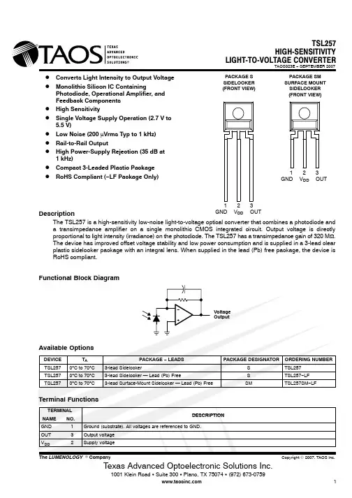
D Converts Light Intensity to Output Voltage D Monolithic Silicon IC Containing Photodiode, Operational Amplifier, and Feedback Components D High SensitivityD Single Voltage Supply Operation (2.7 V to 5.5 V)D Low Noise (200 μVrms Typ to 1 kHz)D Rail-to-Rail OutputD High Power-Supply Rejection (35 dB at 1 kHz)D Compact 3-Leaded Plastic Package DRoHS Compliant (−LF Package Only)DescriptionThe TSL257 is a high-sensitivity low-noise light-to-voltage optical converter that combines a photodiode and a transimpedance amplifier on a single monolithic CMOS integrated circuit. Output voltage is directly proportional to light intensity (irradiance) on the photodiode. The TSL257 has a transimpedance gain of 320 M Ω.The device has improved offset voltage stability and low power consumption and is supplied in a 3-lead clear plastic sidelooker package with an integral lens. When supplied in the lead (Pb) free package, the device is RoHS compliant.Functional Block DiagramPACKAGE S SIDELOOKER (FRONT VIEW)1GND2V DD3OUTPACKAGE SM SURFACE MOUNT SIDELOOKER (FRONT VIEW)1GND2V DD3OUTTSL257HIGH-SENSITIVITYLIGHT-TO-VOLTAGE CONVERTERAbsolute Maximum Ratings over operating free-air temperature range (unless otherwise noted)†Supply voltage, V DD (see Note 1) 6 V . . . . . . . . . . . . . . . . . . . . . . . . . . . . . . . . . . . . . . . . . . . . . . . . . . . . . . . . . . . . . Output current, I O ±10 mA. . . . . . . . . . . . . . . . . . . . . . . . . . . . . . . . . . . . . . . . . . . . . . . . . . . . . . . . . . . . . . . . . . . . . . Duration of short-circuit current at (or below) 25°C 5 s . . . . . . . . . . . . . . . . . . . . . . . . . . . . . . . . . . . . . . . . . . . . . . Operating free-air temperature range, T A −25°C to 85°C . . . . . . . . . . . . . . . . . . . . . . . . . . . . . . . . . . . . . . . . . . . . Storage temperature range, T stg −25°C to 85°C . . . . . . . . . . . . . . . . . . . . . . . . . . . . . . . . . . . . . . . . . . . . . . . . . . . . Lead temperature 1,6 mm (1/16 inch) from case for 10 seconds (S Package) 260°C . . . . . . . . . . . . . . . . . . . . Reflow solder, in accordance with J-STD-020C or J-STD-020D (SM Package) 260°C. . . . . . . . . . . . . . . . . . . †Stresses beyond those listed under “absolute maximum ratings” may cause permanent damage to the device. These are stress ratings only, and functional operation of the device at these or any other conditions beyond those indicated under “recommended operating conditions” is not implied. Exposure to absolute-maximum-rated conditions for extended periods may affect device reliability.NOTE 1:All voltages are with respect to GND.Recommended Operating ConditionsMINMAX UNIT Supply voltage, V DD2.7 5.5V Operating free-air temperature, T A70°CElectrical Characteristics at V DD = 5 V , T A = 25°C, λp = 470 nm, R L = 10 k Ω (unless otherwise noted)(see Notes 2 and 3)PARAMETERTEST CONDITIONSMIN TYPMAX UNIT V D Dark voltageE e = 0015mV V DD = 4.5 V,No Load 4.49V OM Maximum output voltage swing V DD = 4.5 V,R L = 10 k Ω4 4.2V V O Output voltageE e = 1.54 μW/cm 2, λp = 470 nm, Note 51.62 2.4V αVDTemperature coefficient of dark voltage (V D )T A = 0°C to 70°C−15μV/°Cλp = 428 nm, see Notes 4 and 81.18λp = 470 nm, see Notes 5 and 8 1.30N eIrradiance responsivityλp = 565 nm, see Notes 6 and 8 1.58V/(μW/cm 2)λp = 645 nm, see Notes 7 and 81.68PSRR Power supply rejection ratio f ac = 100 Hz, see Note 955dB pp y j f ac = 1 kHz, see Note 935dB I DDSupply currentE e = 1.54 μW/cm 2, λp = 470 nm, Note 51.93.5mA NOTES: 2.Measured with R L = 10 k Ω between output and ground.3.Optical measurements are made using small-angle incident radiation from a light-emitting diode (LED) optical source.4.The input irradiance is supplied by a GaN/SiC light-emitting diode with the following characteristics: peak wavelength λp = 428 nm,spectral halfwidth Δλ½ = 65 nm.5.The input irradiance is supplied by an InGaN light-emitting diode with the following characteristics: peak wavelength λp = 470 nm,spectral halfwidth Δλ½ = 35 nm.6.The input irradiance is supplied by a GaP light-emitting diode with the following characteristics: peak wavelength λp = 565 nm,spectral halfwidth Δλ½ = 28 nm.7.The input irradiance is supplied by an AlGaAs light-emitting diode with the following characteristics: peak wavelength λp = 645 nm,spectral halfwidth Δλ½ = 25 nm.8.Irradiance responsivity is characterized over the range V O = 0.1 V to 4.5 V. The best-fit straight line of Output Voltage V O versusIrradiance E e over this range will typically have a positive extrapolated V O value for E e = 0.9.Power supply rejection ratio PSRR is defined as 20 log (ΔV DD (f)/ΔV O (f)) with V DD (f = 0) = 5 V and V O (f = 0) = 2 V.TSL257HIGH-SENSITIVITYLIGHT-TO-VOLTAGE CONVERTERTAOS023E − SEPTEMBER 2007Switching Characteristics at V DD = 5 V , T A = 25°C, λp = 470 nm, R L = 10 k Ω (unless otherwise noted)PARAMETERTEST CONDITIONS MINTYP MAXUNIT t r Output pulse rise time, 10% to 90% of final value See Note 10 and Figure 1160250μs t f Output pulse fall time, 10% to 90% of final value See Note 10 and Figure 1150250μs t sOutput settling time to 1% of final value See Note 10 and Figure 1330μs Integrated noise voltage f = dc to 1 kHz E e = 0200μVrmsf = 10 Hz E e= 06V Output noise voltage, rms f = 100 Hz E e = 06V/√Hz rmsnp g ,f = 1 kHzE e = 07μ/NOTE 10:Switching characteristics apply over the range V O = 0.1 V to 4.5 V.VOLTAGE WAVEFORMTEST CIRCUITInputE e 10%90%Output (see Note B)t r Outputt f90%10%NOTES: A.The input irradiance is supplied by a pulsed InGaN light-emitting diode with the following characteristics: λp = 470 nm,t r < 1 μs, t f < 1 μs.B.The output waveform is monitored on an oscilloscope with the following characteristics: t r < 100 ns, Z i ≥ 1 M Ω, C i ≤ 20 pF.Figure 1. Switching TimesTSL257HIGH-SENSITIVITYLIGHT-TO-VOLTAGE CONVERTERTAOS023E − SEPTEMBER 2007TYPICAL CHARACTERISTICSFigure 20.60300500700900R e l a t i v e R e s p o n s i v i t y1.211001.00.80.4λ − Wavelength − nm0.21.41.6PHOTODIODE SPECTRAL RESPONSIVITYFigure 320080604010 f − Frequency − Hz10102106105104103P o w e r S u p p l y R e j e c t i o n R a ti o — d B307050POWER SUPPLY REJECTION RATIOvsFREQUENCYFigure 4421010DARK VOLTAGEvsFREE-AIR TEMPERATURE− D a r k V o l t a g e − m VV D 3T A − Free-Air Temperature − °C97658Figure 50NORMALIZED RESPONSEvsANGULAR DISPLACEMENT−90−70−50−3010305070900.10.20.30.40.50.60.70.80.91.0N o r m a l i z e d R e s p o n s e−10Angular Displacement − 5TSL257HIGH-SENSITIVITYLIGHT-TO-VOLTAGE CONVERTERTAOS023E − SEPTEMBER 2007APPLICATION INFORMATIONPCB Pad LayoutSuggested PCB pad layout guidelines for the SM surface mount package are shown in Figure 6.NOTES: A.All linear dimensions are in millimeters.B.This drawing is subject to change without notice.Figure 6. Suggested SM Package PCB LayoutTSL257HIGH-SENSITIVITYLIGHT-TO-VOLTAGE CONVERTERTAOS023E − SEPTEMBER 2007MECHANICAL DATAThe device is supplied in a clear plastic three-lead sidelooker through-hole package (S). PACKAGE S PLASTIC SINGLE-IN-LINE SIDE-LOOKER PACKAGE2TOP VIEWSIDE VIEWFRONT VIEWLead Free AvailablePbNOTES: A.All linear dimensions are in millimeters; tolerance is ± 0.25 mm unless otherwise stated.B.Dimension is to center of lens arc, which is located below the package face.C.The integrated photodiode active area is round with a typical diameter of 0.75 mm and is typically located in the center of the lensand 0.97 mm below the top of the lens surface.D.Index of refraction of clear plastic is 1.55.E.Lead finish for TSL257: solder dipped, 63% Sn/37% Pb. Lead finish for TSL257−LF: solder dipped, 100% Sn.F.This drawing is subject to change without notice.Figure 7. Package S — Single-In-Line Side-Looker Package ConfigurationTSL257HIGH-SENSITIVITYLIGHT-TO-VOLTAGE CONVERTERTAOS023E − SEPTEMBER 2007MECHANICAL DATAPACKAGE SM PLASTIC SURFACE MOUNT SIDE-LOOKER PACKAGETOP VIEWSIDE VIEWFRONT VIEWNOTES: A.All linear dimensions are in millimeters; tolerance is ± 0.25 mm unless otherwise stated.B.Dimension is to center of lens arc, which is located below the package face.C.The integrated photodiode active area is typically located in the center of the lens and 0.97 mm below the top of the lens surface.D.Index of refraction of clear plastic is 1.55.E.Lead finish for TSL257SM −LF: solder dipped, 100% Sn.F.This drawing is subject to change without notice.Figure 8. Package SM — Surface Mount Side-Looker Package ConfigurationTSL257HIGH-SENSITIVITYLIGHT-TO-VOLTAGE CONVERTERTAOS023E − SEPTEMBER 2007PRODUCTION DATA — information in this document is current at publication date. Products conform to specifications in accordance with the terms of Texas Advanced Optoelectronic Solutions, Inc. standard warranty. Production processing does not necessarily include testing of all parameters.LEAD-FREE (Pb-FREE) and GREEN STATEMENTPb-Free (RoHS) TAOS’ terms Lead-Free or Pb-Free mean semiconductor products that are compatible with the current RoHS requirements for all 6 substances, including the requirement that lead not exceed 0.1% by weight in homogeneous materials. Where designed to be soldered at high temperatures, TAOS Pb-Free products are suitable for use in specified lead-free processes.Green (RoHS & no Sb/Br) TAOS defines Green to mean Pb-Free (RoHS compatible), and free of Bromine (Br) and Antimony (Sb) based flame retardants (Br or Sb do not exceed 0.1% by weight in homogeneous material).Important Information and Disclaimer The information provided in this statement represents TAOS’ knowledge and belief as of the date that it is provided. TAOS bases its knowledge and belief on information provided by third parties,and makes no representation or warranty as to the accuracy of such information. Efforts are underway to better integrate information from third parties. TAOS has taken and continues to take reasonable steps to provide representative and accurate information but may not have conducted destructive testing or chemical analysis on incoming materials and chemicals. TAOS and TAOS suppliers consider certain information to be proprietary, and thus CAS numbers and other limited information may not be available for release.NOTICETexas Advanced Optoelectronic Solutions, Inc. (TAOS) reserves the right to make changes to the products contained in this document to improve performance or for any other purpose, or to discontinue them without notice. Customers are advised to contact TAOS to obtain the latest product information before placing orders or designing TAOS products into systems.TAOS assumes no responsibility for the use of any products or circuits described in this document or customer product design, conveys no license, either expressed or implied, under any patent or other right, and makes no representation that the circuits are free of patent infringement. TAOS further makes no claim as to the suitability of its products for any particular purpose, nor does TAOS assume any liability arising out of the use of any product or circuit, and specifically disclaims any and all liability, including without limitation consequential or incidental damages.TEXAS ADVANCED OPTOELECTRONIC SOLUTIONS, INC. PRODUCTS ARE NOT DESIGNED OR INTENDED FOR USE IN CRITICAL APPLICATIONS IN WHICH THE FAILURE OR MALFUNCTION OF THE TAOS PRODUCT MAY RESULT IN PERSONAL INJURY OR DEATH. USE OF TAOS PRODUCTS IN LIFE SUPPORT SYSTEMS IS EXPRESSLY UNAUTHORIZED AND ANY SUCH USE BY A CUSTOMER IS COMPLETELY AT THE CUSTOMER’S RISK.LUMENOLOGY, TAOS, the TAOS logo, and Texas Advanced Optoelectronic Solutions are registered trademarks of Texas Advanced Optoelectronic Solutions Incorporated.。
TSPL2指令集中文肯定Revise History目錄表DOCUMENT CONVENTIONS................................................................................................. .................. I SETUP AND SYSTEM COMMANDS.. (1)SIZE (1)GAP (2)BLINE (4)OFFSET (5)SPEED (6)DENSITY (7)DIRECTION AND MIRROR IMAGE (8)REFERENCE (9)COUNTRY (10)CODEPAGE (11)CLS (12)FEED (13)BACKFEED (14)FORMFEED (15)HOME (16)PRINT (17)SOUND (18)CUT (19)LIMITFEED (20)SELFTEST (21)CONFIG (22)LABEL FORMATTING COMMANDS (23) BAR (23)BARCODE (24)BITMAP (28)BOX (30)DMATRIX (31)ERASE (32)MAXICODE (33)PDF417 (35)PUTBMP (39)PUTPCX (40)QRCODE (41)REVERSE (44)TEXT (45)STATUS POLLING COMMANDS (RS-232) (47) !? (47)!R (48)~!@ (49)~!A (50)~!C (51)~!D (52)~!F (53)~!I (54)~!T (55)MESSAGE TRANSLATION PROTOCOLS (56) ~# (56)COMMANDS FOR WINDOWS DRIVER (57) !B (57)!J (58)!N (59)FILE MANAGEMENT COMMANDS (60) EOP (62)FILES (63)KILL (64)MOVE (65)RUN (66)BASIC COMMANDS AND FUNCTIONS (67) ABS( ) (67)ASC( ) (68)CHR$( ) (69)END (70)EOF( ) (71)OPEN (72)READ (74)SEEK (76)LOF( ) (77)FREAD$( ) (78)FOR...NEXT .. (79)IF...THEN...ELSE...ENDIF. (80) GOSUB...RETURN .. (83)GOTO (84)INP$( ) (85)INPUT (86)REM (87)OUT (88)GETKEY( ) (89)INT( ) (90)LEFT$( ) (91)LEN( ) (92)MID$( ) (93)RIGHT$( ) (94)STR$( ) (95)VAL( ) (96)BEEP (97)DEVICE RECONFIGURATION COMMANDS (98) SET COUNTER (98)SET CUTTER (99)SET PARTIAL_CUTTER (100)SET BACK (101)SET KEY1, SET KEY2, SET KEY3 (102)SET LED1, SET LED2, SET LED3 (104)SET PEEL (105)SET TEAR (106)SET GAP (107)SET HEAD (109)SET RIBBON (110)SET COM1 (111)SET PRINTKEY (112)SET REPRINT (114)PEEL (115)LED1, LED2, LED3 (116)KEY1, KEY2, KEY3 (117)PRINTER GLOBAL VARIABLES (118)@LABEL (118)YEAR (119)MONTH (120)DATE (121)HOUR (123)MINUTE (124)SECOND (125)@YEAR (126)@MONTH (127)@DATE (128)@DAY (129)@HOUR (130)@MINUTE (131)@SECOND (132)文件中的习惯用法此手冊中出現的习惯用法。
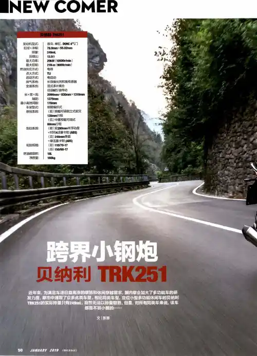
■NEW COMER制动系统:轮胎规格:燃油箱容积:净质量:长X宽X高:轴距:最小离地间隙:车架鹹 悬挂系统:贝纳利发动缸径X 冲程:排量: 压缩比: 最大功率: 最大扭矩: 燃油供应方式:点火旗: 启动丑: 排气磁 变速系统:液冷,单缸 78.0mmx<249mL 12.0:12OkW (1O5 21N-m (90 电喷TU电启动 长效催化帛 世多片帝 越殆铤 2090mm x 1375mm 170mm 钢管编织丘(前)预载135nwn^^(后)中置60mm^(前)双2C +对触活(后)240! +单活塞V(前)112 (后)150/18L 160kgNEW COMER车海领航高离地间隙41mm和中器揺臂你即差路况从开启新世界仅从排量来看,称TRR251为“入门级”是正确的,但这款源于贝纳利的特色车型绝对不是一款简单的入门级多功能车,哪怕是大哥rRK502也无法遮蔽它的光芒。
此车搭载了源于"小黄龙”的单缸液冷DOHC4气门高压缩比发动机,设置了内置平衡轴,采用可靠的电喷系统、TLI点火,爆发力强、运转平稳,国四排放、往返式6挡变速,而最大功率20.0k\\(105()0r/min)、最大扭矩21.0N-m (9000r/min)极速超ill30km/h的性能表现,也让同级别对手无法骄傲。
52JANUARY2019《摩托车杂志》NEW COMER车海领航TRK251的车型定位是“轻量级”,厂家在车身规格、自重等方面掌握着尺度,尽可能地让这款面向新手的车型轻灵而易于掌控,2090m m的整车长度和1375m m的轴距设定显然是适中的。
在整体框架上,该车仍沿用已在之前车款上得到验证的钢管编织车架,整车的刚性值得信赖。
整体压铸的轻量化轮網配前11()7()-17>后15060-17规格的真空胎,具有较强的路况适应能力。
在悬挂系统,前悬挂4limn的直径属于同级别之最了,再加上120mm的有效行程,完全能够胜任整车“全地形”的性能需求。

Two Hardworking Chain Saws Promoted to Legendary BOSSStatusNext Generation of STIHL Boss Chain Saws Packed with ProfessionallyInspired FeaturesRelease Date: 3/12/2015Press Inquiries:Lindsy Shrewsberry(757) 4869286All other inquiries:STIHL Incorporated(757) 4869100VIRGINIA BEACH, Va. – For years, the legendary Boss name has been synonymous with premium quality at an affordable price with the power to get the job done. Two of the most popular STIHL chain saws, the STIHL MS 251 WOOD BOSS® and MS 271 FARM BOSS®, are the latest to bear the Boss titles.“These chain saws are built in America* and include some of our latest innovations,” said Kent Hall, senior product manager at STIHL Inc. “These two hardworking saws have the power and performance features that our customers want, at a price point that fits their budget.”MS 251 WOOD BOSS®Power meets high efficiency to make quick work of felling small trees, pruning, thinning and cutting firewood. Packed with 45.6 cc of legendary STIHL quality and dependability, the MS 251 WOOD BOSS® makes work go faster so homeowners and professionals can move on to the next project on their list. Boasting up to 20 percent better fuel efficiency,** this affordablypriced workhorse also saves money at the pump.Its preseparation air filtration technology boosts the efficiency of the engine’s filter system resulting in less frequent cleaning and replacement. In cold temperatures, the winter/summer shutter can be switched to “winter” to help the saw operate at optimum temperature and prevent carburetor icing.MS 271 FARM BOSS®A true powerhouse, the 50.2 cc MS 271 FARM BOSS® takes charge when it comes time for felling, cutting firewood, or storm cleanup. It tackles cutting jobs with a lowemission, fuelefficient engine that gets the job done with lower fuel costs. A powerful legend in the making, the FARM BOSS® produces 50 percent lower emissions, reduces fuel consumption and delivers up to 20 percent longer run times on a tank of fuel as compared to similar traditional 2stroke STIHL chain saws. Its preseparation air filtration system can extend filter life up to five times longer.Designed with comfort in mind for farmers, rural landowners, and tree farmers, the FARM BOSS® is equipped with a compact design providing optimum control when working. An advanced antivibration system provides comfortable operation and reduces fatigue.For more information on the STIHL MS 251 WOOD BOSS® and MS 271 FARM BOSS® visit:.*A majority of STIHL powerheads are built in the United States from domestic and foreign parts and components.**As compared to previous STIHL models in the same range.About STIHL Inc.STIHL Inc. manufactures the number one selling brand of gasolinepowered handheld outdoor power equipment in America,* as well as the number one selling brand of chain saws in the world. STIHL products are sold through servicing power equipment retailers from coast to coast – not mass merchants. Located in Virginia Beach, Va., STIHL Inc., the headquarters for U.S. operations for the worldwide STIHL Group, exports to over 90 countries around the world; and the majority of STIHL products sold in America are also built in America.* STIHL products sold through U.S. STIHL dealers are for distribution in the United States only. For more information or for the name of a local STIHL retailer, call toll free 1800GO STIHL (18004678445), visit or text your zip code to 78445.*A majority of STIHL powerheads are built in the United States from domestic and foreign parts and components. "Number one selling brand" is based on syndicated Irwin Broh Research as well as independent consumer research of 20092014 U.S. sales and market share data for the gasolinepowered handheld outdoor power equipment category combined sales to consumers and commercial landscapers.STIHL is pleased to support the work of Independent We Stand, the Tree Research and Education Endowment Fund (TREE Fund), International Society of Arboriculture (ISA), the Tree Care Industry Association (TCIA), National FFA, National Association of Landscape Professionals, the National Recreation and Parks Association, the National Association of State Park Directors and the North American Retail Hardware Association.For information on job opportunities with STIHL Inc., please go to . STIHL is an EEO and drugfree work environment.# # #MS 271 FARM BOSS® Specifications MidRange Use DISPLACEMENT50.2 cc (3.06 cu. in.) ENGINE POWER 2.6 kW (3.49 bhp) POWERHEAD WEIGHT 5.6 kg (12.3 lbs.) FUEL CAPACITY500 cc (16.9 oz.) CHAIN OIL CAPACITY240 cc (8.12 oz.) OILOMATIC® CHAIN26 RM3GUIDE BAR LENGTHS* (Recommended ranges)40 to 50 cm (16" to 20") STIHL ROLLOMATIC®POWER SOURCE GasSTIHL recommends #3634 (26 RM3 67) OILOMATIC® saw chain and 16" 3003 812 6813 Ematic™ guide bar combination. The actual listed guide bar length can vary from the effective cutting length depending upon which powerhead it is installed.。
采用光强传感器J N5139和T S L2561的光强传感器节点设计农业生产、气象环保等工作中,光照强度是环境监测中的重要参数;尤其是在温室大棚中,光强对作物有着决定性的作用。
为了实现对光强的监测,本文选用高速、可编程芯片T S L2561作为光强传感器,对光照强度进行测量。
微处理器采用英国J e n n i c公司推出的高性能、低功耗、高速率无线芯片J N5139。
该芯片集处理器、收发器于一体,通过无阻塞设计大大提高了C P U利用率,与传统的有线设备相比,具有灵活性高、成本低、可维护性高等优点。
1T S L2561的内部结构及工作原理T S L2561[1]是T A O S公司推出的第二代光强数字转换芯片,具有高速、低功耗、宽量程、可编程灵活配置等优点。
T S L2561具有直接I2C 接口,用于将光照强度转换成数字信号输出。
其内部结构如图1[2]所示。
T S L2561内部连接一个光敏二极管(通道0)和一个红外响应光敏二极管(通道1)。
这个集成电路具有提供20位动态范围内近适光响应的能力。
两个集成的积分式A/D转换器,可将光敏电流转换成一个数字输出,并存入芯片内部通道0和通道1各自的寄存器中。
数字输出表示测量每一个通道的光强,可以是微处理器的输入。
T S L2561可直接通过I2C总线协议由微控制器访问,微控制器则通过对其内部的16个寄存器的读写来实现对T S L2561的控制。
图1T S L2561内部结构图2硬件设计微处理器采用J e n n i c公司推出的高速率、低功耗、低成本J N5139无线S o C芯片[3]。
该芯片集成了一个32位R I S C处理器,可充分兼容2.4G H z I E E E802.15.4收发器,具有192K B的R O M和8~96K B内可选的R A M,提供丰富的模拟量和数字外围设备接口。
J N5139芯片带有I2C总线控制器,只需将该总线的时钟线和数据线直接与T S L2561的I2C总线的S C L和S D A线分别相连。
ISO5211-2001中⽂版通⽤阀门-部分回转阀门驱动装置Reference number ISO 5211:2001(E)ISO 2001INTERNATIONAL STANDARD ISO 5211First edition 2001-02-15Industrial valves —Part-turn actuator attachmentRobinetterie industrielle — Raccordement des actionneurs à fraction de tour--`,,`,-`-`,,`,,`,`,,`---ISO5211:2001(E)PDF disclaimerThis PDF file may contain embedded typefaces.In accordance with Adobe's licensing policy,this file may be printed or viewed but shall not be edited unless the typefaces which are embedded are licensed to and installed on the computer performing the editing.In downloading this file,parties accept therein the responsibility of not infringing Adobe's licensing policy.The ISO Central Secretariat accepts no liability in this area.Adobe is a trademark of Adobe Systems Incorporated.Details of the software products used to create this PDF file can be found in the General Info relative to the file;the PDF-creation parameters were optimized for printing.Every care has been taken to ensure that the file is suitable for use by ISO member bodies.In the unlikely event that a problem relating to it is found,please inform the Central Secretariat at the address given below.--`,,`,-`-`,,`,,`,`,,`---ISO2001All rights reserved.Unless otherwise specified,no part of this publication may be reproduced or utilized in any form or by any means,electronic or mechanical,including photocopying and microfilm,without permission in writing from either ISO at the address below or ISO's member body in the country of the requester.ISO copyright officeCase postale56·CH-1211Geneva20Tel.+41227490111Fax+41227490947E-mail copyright@iso.chWeb www.iso.chPrinted in SwitzerlandISO5211:2001(E)ForewordISO(the International Organization for Standardization)is a worldwide federation of national standards bodies(ISO member bodies).The work of preparing International Standards is normally carried out through ISO technical committees.Each member body interested in a subject for which a technical committee has been established has the right to be represented on that committee.International organizations,governmental and non-governmental,in liaison with ISO,also take part in the work.ISO collaborates closely with the International Electrotechnical Commission(IEC)on all matters of electrotechnical standardization.International Standards are drafted in accordance with the rules given in the ISO/IEC Directives,Part3.Draft International Standards adopted by the technical committees are circulated to the member bodies for voting. Publication as an International Standard requires approval by at least75%of member bodies casting a vote. Attention is drawn to the possibility that some of the elements of this International Standard may be the subject of patent rights.ISO shall not be held responsible for identifying any or all such patent rights.International Standard ISO5211was prepared by the European Committee for Standardization(CEN)in collaboration with ISO Technical Committee TC153,Valves,Subcommittee SC2,Valve actuator attachment,in accordance with the Agreement on technical cooperation between ISO and CEN(Vienna Agreement). Throughout the text of this standard,read"...this European Standard..."to mean"...this International Standard...".This first edition of ISO5211cancels and replaces ISO5211-1:1977,ISO5211-2:1979and ISO5211-3:1982, which have been technically revised.ISO5211:2001(E)--`,,`,-`-`,,`,,`,`,,`---ContentsPage Foreword (v)1Scope (1)2Normative references (2)3Terms and definitions (2)4Maximum flange torques (2)5Flange dimensions (3)6Designation (5)7Dimensions and torques (6)7.1General (6)7.2Drive by key(s) (6)7.3Drive by parallel or diagonal square head (9)7.4Drive by flat head (10)8Position of driven components at interface below part-turn actuator (11)8.1Drive by key(s) (11)8.2Drive by parallel or diagonal square head (12)8.3Drive by flat head (13)Bibliography (14)ISO5211:2001(E)ForewordThe text of EN ISO5211:2001has been prepared by Technical Committee CEN/TC69"Industrial valves",the secretariat of which is held by AFNOR,in collaboration with Technical Committee ISO/TC153"Valves".This European Standard shall be given the status of a national standard,either by publication of an identical text or by endorsement,at the latest by August2001,and conflicting national standards shall be withdrawn at the latest by August2001.This European Standard currently includes actuators with key(s),square and flat drives.Other types of drives may be included in the future.--`,,`,-`-`,,`,,`,`,,`---This European Standard has been prepared under a mandate given to CEN by the European Commission and the European Free Trade Association.This European Standard is considered to be a supporting standard to those application and product standards which in themselves support an essential safety requirement of a New Approach Directive and which make reference to this European Standard.According to the CEN/CENELEC Internal Regulations,the national standards organizations of the following countries are bound to implement this European Standard:Austria,Belgium,Czech Republic,Denmark,Finland,France,Germany,Greece,Iceland,Ireland,Italy,Luxembourg,Netherlands,Norway,Portugal,Spain,Sweden, Switzerland and the United Kingdom.--`,,`,-`-`,,`,,`,`,,`---ISO 5211:2001(E)1ScopeThis European Standard specifies requirements for the attachment of part-turn actuators,with or without gearboxes,to industrial valves.The attachment of part-turn actuators to control valves is in accordance with the requirements of this standard only when subject to an agreement between the supplier and the purchaser.This standard specifies :?flange dimensions necessary for the attachment of part-turn actuators to industrial valves (see Figure 1a)or to intermediate supports (see Figure 1b);driving component dimensions of part-turn actuators necessary to attach them to the driven components ;reference values for torques for interfaces and for couplings having the dimensions specified in this standard.The attachment of the intermediate support to the valve is not the subject of this standard.NOTE 1In this standard the term “valve ”may also be understood to include “valve with an intermediate support ”(see Figure1).NOTE 2When the part-turn actuator is a combination of a multi-turn actuator and a gearbox,the multi-turn actuator attachment to the gearbox should be in accordance with EN ISO 5210.Key1Part-turn actuator 2Interface 3Valve4Intermediate supportFigure 1-Direct and intermediate support interfaces--`,,`,-`-`,,`,,`,`,,`---ISO5211:2001(E)2Normative referencesThis European Standard incorporates by dated or undated reference,provisions from other publications.These normative references are cited at the appropriate places in the text and the publications are listed hereafter.For dated references,subsequent amendments to or revisions of any of these publications apply to this European standard only when incorporate in it by amendments or revision.For undated references,the latest edition of the publication referred to applies(including amendments).ISO273,Fasteners-Clearance holes for bolts and screws.ISO/TR773,Rectangular or square parallel keys and their corresponding keyways(dimensions in millimetres).3Terms and definitionsFor the purposes of this European Standard,the following terms and definitions apply:3.1actuatorany power operated device used to operate a valve.The device is designed to operate using motive energy which may be electrical,pneumatic,hydraulic,etc.,or a combination of these.Movement is limited by travel,torque or thrust3.2part-turn actuatoractuator which transmits torque to the valve for a rotation of one revolution or less.It does not have to be capable of withstanding axial thrust3.3gearboxany mechanism designed to reduce the torque required to operate a valve3.4torqueturning moment transmitted through the mounting flanges and connection components.It is expressed in Newton-metres(Nm) 4Maximum flange torquesThe maximum flange torque values listed in Table1give the maximum torques which can be transmitted through the mounting flange.--`,,`,-`-`,,`,,`,`,,`---ISO5211:2001(E)Table1-Maximum flange torque valuesFlange type Maximum flange torqueNmF0332F0463F05125F07250F10500F121000F142000F164000F258000F3016000F3532000F4063000F48125000F60250000The values specified in Table1have been defined on the basis of bolts in tension only at a stress of290MPa1 and a coefficient of friction of0,2between the mounting interface.All variations in these defined parameters lead to variations of the transmittable torque values.The selection of flange types for a particular application should take into account the additional torques that may be generated because of inertia or other factors.5Flange dimensionsFlanges for part-turn actuator attachments shall comply with the dimensions shown in Figure2and given in Table2.The method of attachment shall be by means of studs,screws or through bolting.When through bolting is used,the diameter of the clearance holes shall permit the use of bolts of a size given by the corresponding dimension d4in Table2.Holes for the studs,screws or bolts shall be equi-spaced and positioned off-centre(see Figure3and Table3),and shall conform to the requirements of ISO273.The flange on the valve shall have a recess corresponding to the diameter d2;a spigot on the part-turn actuator is optional. The minimum values for dimension h2apply to flanges having material of proof stress R p0,23200MPa.Dimension d1has been calculated to provide sufficient seating for nuts and bolt heads.Such seating is defined as a radiusfrom the bolt hole centre with the dimension(d1-d3)/2,and is a minimum.The flange shape and the design of the mounting surface of the valve and part-turn actuator outside these areas of seating is left to the choice of the manufacturer.11MPa=1N/mm2--`,,`,-`-`,,`,,`,`,,`---ISO5211:2001(E)Key1Part-turn actuatorFigure2-Flange dimensionsTable2-Flange dimensionsDimensions in millimetresFlange type d1d2f8d3d4h1max.h2min.Number of screws, studs orboltsF03462536M5384 F04543042M5384 F05653550M6394 F07905570M83124 F1012570102M103154F1215085125M123184 F14175100140M164244 F16210130165M205304 F25300200254M165248F30350230298M205308 F35415260356M305458 F40475300406M368548 F48560370483M3685412F60686470603M3685420ISO5211:2001(E)Figure3-Position of holesTable3-Position of holesFlange type=/2F03to F1645°F25to F4022,5°F4815°F609°6DesignationPart-turn valve actuator attachments shall be designated as follows:flange designation:flange type as per Table1;a capital letter for spigot identification:Y with spigot;N without spigot;drive designation:an additional capital letter for drive identification:V for single key drive;W for two key drive;L for parallel square drive;D for diagonal square drive;H for flat head drive;ISO5211:2001(E)the actual dimensions of the drive(in millimetres):dimension d7for key drives(see Figure4and Table4);dimension s for square or flat drives(see Figures5or6and Table5or Figure7and Table6). EXAMPLEEN ISO5211–F05–Y–V–1818mm diameterFlange typeY=with spigotN=without spigot V=single key driveW=two key driveL=parallel square drive D=diagonal square drive H=flat head driveEN ISO5211-F05-Y-V-18,identifies a part-turn valve actuator attachment in accordance with this standard, with F05flange type,spigot and single key drive with18mm diameter.NOTE The designation is not a marking requirement.7Dimensions and torques7.1GeneralTo ensure that no interference can occur between the driving component and the driven component,the length of the driven component above the interface shall be limited so that there is a clearance between both parts.7.2Drive by key(s)Dimensions of drive components for key drive shall meet the requirements of Figure4and Table4.The values of d7,h4and l5in Table4are based on single key design up to98mm shaft diameter.Where more than one key is required to transmit the torque,the dimensions in Table4shall still apply.The key dimensions shall comply with those given in ISO/TR773.The keyway(s)in the driving component shall correspond to the position of the key(s)supplied on the driven component as specified in8.1,Figures8or9.The key(s)shall be secured in position by suitable means.--`,,`,-`-`,,`,,`,`,,`---ISO 5211:2001(E)Key1InterfaceFigure 4-Drive by key(s)--`,,`,-`-`,,`,,`,`,,`---T a b l e 4-D i m e n s i o n s a n d t o r q u e s f o r d r i v e b y k e y (s )D i m e n s i o n s i n m i l l i m e t r e sF l a n g e t y p e M a x .f l a n g e t o r q u e N mh 4m a x .f l 5m i n .d 7H 9a bF 051253,030121418c22---------------F 072503,035-141822c 28--------------F 105003,045--182228c 3642------------F 1210003,055---222836c 424850---------F 1420005,065----28364248c5060---------F 1640005,080-----42485060c7280-------F 2580005,0110-------48506072c8098100-----F 30160005,0130---------60728098c100120----F 35320005,0180--------------160---F 40630008,0200----------------180--F 481250008,0250-----------------220-F 602500008,0310-----------------280M a x .t r a n s m i s s i b l e t o r q u e N m d 32631252505001000150020003000400080001200016000e e e eeea F o r f l a n g e t y p e s F 05t o F 30o t h e r d i m e n s i o n s o f d 7b e t w e e n t h o s e i n d ic a t ed a re p e r m i t t e df o r a m a x i m u m o f 5y e a r s a f t e r t h e p u b l i c a t i o n o f t h i s s t a n d a r d .bF o r f l a n g e t y p e s a b o v e F 30,t h e d 7v a l u e s g i v e n i s t h e m a x i m u m a n d a n y v a l u e u p t o t h i s m a x i m u m i s p e r m i t t e d ,s u b j e c t t o c o n s i d e r a t i o n s i n d b e l o w .cI n d i c a t e s t h e p r e f e r r e d d i m e n s i o n .dF o r f l a n g e t y p e s F 05t o F 30,t h e s e a r e t h e c o r r e s p o n d i n g t o r q u e s w h i c h c a n b e t r a n s m i t t e d b y t h e d r i v i n g c o m p o n e n t s h a v i n g t h e d 7d i m e n s i o n s .T h e y a r e b a s e d o n a m a x .a l l o w a b l e t o r s i o n a l s t r e s s o f 280M P a f o r t h e d r i v e n c o m p o n e n t ,a m a x .c o m p r e s s i v e s t r e s s o n t h e k e y o f 350M P a a n d a n e f f e c t i v e l e n g t h o f k e y e n g a g e m e n t e q u a l t o (l 5-h 4).eT h e m a x i m u m t r a n s m i s s i b l e t o r q u e s s h a l l b e d e t e r m i n e d b y c a l c u l a t i o n .fh 4m i n .=0,5m m .ISO 5211:2001(E)--`,,`,-`-`,,`,,`,`,,`---ISO 5211:2001(E)7.3Drive by parallel or diagonal square headDimensions of drive components for square heads shall meet the requirements of Figures 5or 6and Table 5.The choice of d 8and d 9depends on the manufacturing process.The square drive positions shall be as specified in 8.2,Figures 10or 11.Key1InterfaceFigure 5-Drive by parallel square head Figure 6-Drive by diagonal square headTable 5-Dimensions and torques for drive by parallel or diagonal square headDimensions in millimetresFlange type Max.flange torqueNmh 4max.as H11F03321,59---------F04631,5911b ---------F051253,091114b --------F072503,0-111417b -------F105003,0--14171922b -----F1210003,0---17192227b ----F1420005,0-----222736b ---F1640005,0------273646b --F2580005,0-------364655b -F30160005,0--------465575b ?d 8min.12,114,118,122,225,228,236,248,260,272,298,2?d 9max.9,511,614,717,92023,128,43848,557,979,1l 5min 1012161921242938485777Max.transmissible torque Nm c3263125250350500100020004000800016000a h 4min.=0,5mm.b Indicates the preferred dimension.cMaximum transmissible torques are based on a maximum allowable torsional stress of 280MPa for the driven component. --`,,`,-`-`,,`,,`,`,,`---ISO 5211:2001(E)7.4Drive by flat headDimensions of drive components for flat head drive shall meet the requirements of Figure 7and Table 6.The flat head drive position shall be as specified in 8.3,Figure 12.Key 1InterfaceFigure 7-Drive by flat headTable 6-Dimensions and torques for drive by flat headDimensions in millimetresFlange typeMax.flange torque Nmh 4max.as H11F03321,59----------F04631,5911b ---------F051253,091114b --------F072503,0-111417b -------F105003,0-14171922b -----F1210003,0---17192227b ----F1420005,0-----222736b ---F1640005,0------273646b --F2580005,0-------364655b F30160005,0 -------465575bd 8min.12,114,118,122,225,228,236,248,260,272,298,2l 5min.16192530343948648299135Max.transmissible torque Nm c3263125250350500100020004000800016000ah 4min.=0,5mmb Indicates the preferred dimensioncMaximum transmissible torques are based on a maximum allowable torsional stress of 280MPa for the driven component --`,,`,-`-`,,`,,`,`,,`---ISO 5211:2001(E)8Position of driven components at interface below part-turn actuator8.1Drive by key(s)One or two keys may be used.With the valve closed the key(s)shall be located as shown in Figures 8or 9.If more than two keys are required,their position shall be subject to an agreement between the supplier and the purchaser.NOTEThe standard closing direction is clockwise,as viewed from above the interface.Key1Opening direction 2Primary keyFigure 8–Position of primary key on the driven componentKey1Opening direction 2Primary key 3Secondary keyFigure 9–Positions of primary and secondary keys on the driven component--`,,`,-`-`,,`,,`,`,,`---ISO 5211:2001(E)8.2Drive by parallel or diagonal square headWith the valve closed,the flat sides of the square head drive component shall be located as shown in Figures 10or 11.Key1Opening directionFigure 10–Position of parallel square head driven componentKey1Opening directionFigure 11–Position of diagonal square head driven component--`,,`,-`-`,,`,,`,`,,`---ISO5211:2001(E)8.3Drive by flat headWith the valve closed,the flat sides of the flat head drive component shall be located as shown in Figure12.Key1Opening directionFigure12-Position of flat head driven component。
3 October 2011FOR IMMEDIATE RELEASECelebrate the full opening of the SMRT Circle Lineon 8 October at Holland Village StationShorter travel times for commuters with the opening of 12 new stations1.SMRT will celebrate the full opening of the Circle Line on 8 October 2011 at Holland Village Station. From 6.00pm to 9.00pm, SMRT will hold a Carnival on the street level with live music and dance performances, stilt walkers, fire twirlers, mardi gras performers and samba percussionists to add to the party atmosphere. Admission is free.2.Commuters can pick up their free copy of an ‘Opening Specials’ discount voucher booklet from any Circle Line station on 8 October*. The booklet contains deals from over 70 merchants from Holland Village and SMRT Xchanges.3.The first 1,000 commuters who present their vouchers at the Carnival will receive a free pint of Tiger beer. Other great deals include free cupcakes from Gastronomia Da Paolo, free nachos and margaritas or a glass of wine from El Patio Restaurant and Wine Bar, as well as discounts of up to 50% from food and beverage, fashion and lifestyle outlets**.4.From 6.00pm to 9.00pm, commuters will be entertained by local bands Matterfour, The Dirt Radicals and Timmy! Band. Adding to the festivities will be "clouds" in the shape of SMRT's logos (customised floating foam that can reach up to 20,000 ft high, weather permitting). Commuters who need to soothe their tired muscles from all that partying can also enjoy foot reflexology and massage services by masseuses from the Singapore Association of the Visually Handicapped.SMRT Corporation Ltd251 North Bridge RoadSingapore 179102 Tel : 65 6331 1000 Fax : 65 6339 4229 .sgMedia ReleaseShorter travel times with newly opened Circle Line stations5. With the opening of the new Circle Line stations, commuters can lookforward to shorter travel times for some journeys via the Circle Line as a result of direct train trips or more convenient train transfers.6. Travel time for commuters using the Circle Line can be shortened by up to17 minutes. For example, commuters travelling from Bishan to HollandVillage will only spend 14 minutes, compared to 31 minutes, using the North-South line and making a transfer by bus. Commuters heading to Bishan from Boon Lay can save 15 minutes by using the Circle Line. It will usually take commuters 34 minutes, using the East-West line then transferring to the Circle Line at Buona Vista Interchange. More examples of how commuters can save travel time with the opening of more Circle Line stations are available in the Annex.- End -Annex。
IMPORTANT NOTICE
Texas Instruments (TI) reserves the right to make changes to its products or to discontinue any semiconductor product or service without notice, and advises its customers to obtain the latest version of relevant information to verify, before placing orders, that the information being relied on is current.
TI warrants performance of its semiconductor products and related software to the specifications applicable at the time of sale in accordance with TI’s standard warranty. Testing and other quality control techniques are utilized to the extent TI deems necessary to support this warranty. Specific testing of all parameters of each device is not necessarily performed, except those mandated by government requirements.
Certain applications using semiconductor products may involve potential risks of death, personal injury, or severe property or environmental damage (“Critical Applications”).
TI SEMICONDUCTOR PRODUCTS ARE NOT DESIGNED, INTENDED, AUTHORIZED, OR WARRANTED TO BE SUITABLE FOR USE IN LIFE-SUPPORT APPLICATIONS, DEVICES OR SYSTEMS OR OTHER CRITICAL APPLICATIONS.
Inclusion of TI products in such applications is understood to be fully at the risk of the customer. Use of TI products in such applications requires the written approval of an appropriate TI officer. Questions concerning potential risk applications should be directed to TI through a local SC sales office.
In order to minimize risks associated with the customer’s applications, adequate design and operating safeguards should be provided by the customer to minimize inherent or procedural hazards.
TI assumes no liability for applications assistance, customer product design, software performance, or infringement of patents or services described herein. Nor does TI warrant or represent that any license, either express or implied, is granted under any patent right, copyright, mask work right, or other intellectual property right of TI covering or relating to any combination, machine, or process in which such semiconductor products or services might be or are used.
Copyright © 1995, Texas Instruments Incorporated。