AIC1727-50CX中文资料
- 格式:pdf
- 大小:127.71 KB
- 文档页数:7
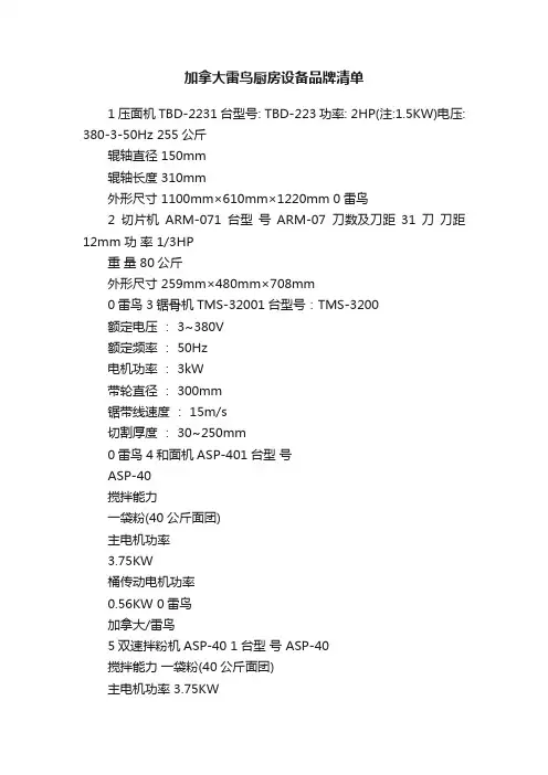
加拿大雷鸟厨房设备品牌清单1压面机TBD-2231台型号: TBD-223功率: 2HP(注:1.5KW)电压: 380-3-50Hz 255公斤辊轴直径 150mm辊轴长度 310mm外形尺寸1100mm×610mm×1220mm 0雷鸟2切片机ARM-071台型号ARM-07刀数及刀距31刀刀距12mm 功率 1/3HP重量 80公斤外形尺寸259mm×480mm×708mm0雷鸟3锯骨机TMS-32001台型号:TMS-3200额定电压: 3~380V额定频率: 50Hz电机功率: 3kW带轮直径: 300mm锯带线速度: 15m/s切割厚度: 30~250mm0雷鸟4和面机ASP-401台型号ASP-40搅拌能力一袋粉(40公斤面团)主电机功率3.75KW桶传动电机功率0.56KW 0雷鸟加拿大/雷鸟5双速拌粉机ASP-40 1台型号 ASP-40搅拌能力一袋粉(40公斤面团)主电机功率 3.75KW桶传动电机功率 0.56KW重量 208公斤外形尺寸848mm×555mm×1155mm 0雷鸟6多功能搅拌机ARM-02 1台型号 ARM-02搅拌能力 20升功率0.56KW重量 98公斤外形尺寸560mm×560mm×850mm 0雷鸟7多功能搅拌机ARM-801台型号 ARM-80搅拌能力 80升功率3.70KW重量 525公斤外形尺寸900mm×720mm×1750mm 0雷鸟8电烤箱TBDO-1200GS 1台型号 TBDO-1200GS 烤盘数量、规格三层九盘功率、电压 24KW 380V 三相外壳材质 #304全不锈钢外形尺寸1080mm×1930mm×1680mm重量 520公斤0雷鸟9多功能搅拌机ARM-601台产品型号: ARM-60产品品牌名称: ARM-60产品竞争优势: 整机由美国机械专家设计,结构精密,高速运转无噪音,搅拌器与桶间隙小,省电、效率高,节省原材料; 60公升多功能搅拌机,设计上为立地式,配合人体工学原理,不用弯腰即可长时间作业。
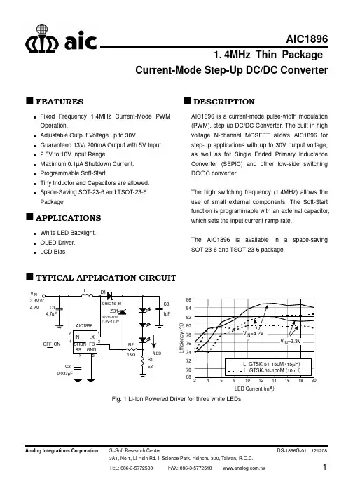
1. 4MHz Thin PackageCurrent-Mode Step-Up DC/DC ConverterAnalog Integrations Corporation Si-Soft Research CenterDS-1896G-01 121208FEATURESFixed Frequency 1.4MHz Current-Mode PWM Operation.Adjustable Output Voltage up to 30V.Guaranteed 13V/ 200mA Output with 5V Input. 2.5V to 10V Input Range.Maximum 0.1µA Shutdown Current. Programmable Soft-Start.Tiny Inductor and Capacitors are allowed.Space-Saving SOT-23-6 and TSOT-23-6 Package.APPLICATIONSWhite LED Backlight. OLED Driver.LCD BiasDESCRIPTIONAIC1896 is a current-mode pulse-width modulation (PWM), step-up DC/DC Converter. The built-in high voltage N-channel MOSFET allows AIC1896 for step-up applications with up to 30V output voltage, as well as for Single Ended Primary Inductance Converter (SEPIC) and other low-side switching DC/DC converter.The high switching frequency (1.4MHz) allows the use of small external components. The Soft-Start function is programmable with an external capacitor, which sets the input current ramp rate.The AIC1896 is available in a space-saving SOT-23-6 and TSOT-23-6 package.TYPICAL APPLICATION CIRCUITµFV IN4.2V687072747678808284862468101214161820LED Current (mA)E f f i c i e n c y (%)Fig. 1 Li-Ion Powered Driver for three white LEDsFV IN4.2VLED Current (mA)E f f i c i e n c y (%)6062646668707274767880Fig. 2 Li-Ion Powered Driver for six white LEDsORDERING INFORMATION& Reel Packing TypeAIC1896PGTRin Lead Free SOT-23-6 Package & Tape& Reel Packing TypeTSOT-23-6 MarkingPart No. Marking AIC1896PK 896PK AIC1896GK896GKSOT-23-6 MarkingPart No. Marking AIC1896PG 1896P AIC1896GG1896GABSOLUTE MAXIMUM RATINGSLX to GND -0.3V to +33V FB to GND -0.3V to +6V IN, SHDN-0.3V to +11V SS to GND -0.3V to +6V LX Pin RMS Current 0.6A Continuous Power Dissipation 727mW Operating Temperature Range -40°C to 85°C Junction Temperature 125°C Storage Temperature Range -65°C to 150°C Lead Temperature (soldering, 10s) 260°CAbsolute Maximum Ratings are those values beyond which the life of a device may be impaired. TEST CIRCUITV IN V OUT10µELECTRICAL CHARACTERISTICSSHDNNote 1: Specifications are production tested at T A=25°C. Specifications over the -40°C to 85°C operating temperature range are assured by design, characterization and correlation with Statistical QualityControls (SQC).TYPICAL PERFORMANCE CHARACTERISTICSFig. 3 Switching Frequency vs. TemperatureS w i t c h i n g F r e q u e n c y (M H z )Temperature (°C)Fig. 4 Frequency vs. Supply VoltageF r e q u e n c y (M H z )Supply Voltage (V)Supply Voltage (V)Fig. 5 R DSON vs. Supply VoltageR D S (O N ) (Ω)Output Current (mA)Fig. 6 Load Regulation (L1=10μH)O u t p u t V o l t a g e (V )Output Current (mA)Fig. 7 Load Regulation (L1=22μH)O u t p u t V o l t a g e (V )Supply Voltage (V)Fig. 8 Switching CurrentS u p p l y C u r r e n t (m A )TYPICAL PERFORMANCE CHARACTERISTICS (Continued)Supply Voltage (V)Fig. 9 Non-Switching CurrentS u p p l y C u r r e n t (μA )Fig. 10Feedback Pin VoltageF e e d b a c k V o l t a g e (V )Temperature (°C)Output Current (mA)Fig. 11 Efficiency vs. Output Current (L1=10µH, test circuit refer to p.3)E f f i c i e n c y (%)Output Current (mA)Fig. 12Efficiency vs. output current (L1=22µH, test circuit refer to p.3)E f f i c i e n c y (%)Fig. 13(a) Maximum Output current vs. Supply Voltage(L1: 10µH, test circuit refer to p.3)M a x i m u m O u t p u t C u r r e nt (m A )Supply Voltage (V)0Fig. 13(b) Maximum Output Current vs. Supply Voltage(L1:22µH, test circuit refer to p.3)M a x i m u m O u t p u t C u r r e n t (m A )Supply Voltage (V)TYPICAL PERFORMANCE CHARACTERISTICS (Continued)Fig. 14 Operation Wave Form(V IN =5V; V OUT =12V, L1=22µH; R1=105K;R2=12K;C3=1nF;I OUT =200mA, test circuit refer to p.3)V OUT V SW ILXFig. 15 Operation Wave Form(V IN =3V;V OUT =5V;L1=10µH;R1=36K;R2=12K; C3=39pF;I OUT =200mA, test circuit refer to p.3)V OUT VLXILXFig. 16 Load Step Response(V IN =3.3V; V OUT =5V;L1=10µH;I OUT =5mA to 200mA,test circuit refer to p.3)V OUTILXFig. 17 Load Step Response(V IN =5V ; V OUT =12V ;L1=22µH;I OUT =5mA to 150mA,test circuit refer to p.3)V OUTI LXFig. 18 Start-Up from Shutdown (V IN =3.3V ;V OUT =13V ;R LOAD =300Ω,test circuit refer to p.3)V OUTSHDN I LXBLOCK DIAGRAMSHDNSSLX FBGND PIN DESCRIPTIONSPIN 1: LX - Power Switching Connection.Connect LX to inductor andoutput rectifier. Keep thedistance between thecomponents as close to LX aspossible.PIN 2: GND - Ground.PIN 3: FB - Feedback Input. Connect aresistive voltage-divider from theoutput to FB to set the outputvoltage.PIN 4: SHDN- Shutdown Input. Drive SHDNlow to turn off the converter. Toautomatically start the converter,connect SHDN to IN. DriveSHDN with a slew rate of0.1V/µs or greater. Do not leaveSHDN unconnected.SHDNdraws up to 50µA.PIN 5: SS - Soft-Start Input. Connect asoft-start capacitor from SS toGND in order to soft-start theconverter. Leave SS open todisable the soft-start function. PIN 6: IN - Internal Bias Voltage Input.Connect IN to the input voltagesource. Bypass IN to GND witha capacitor sitting as close to INas possible.APPLICATION INFORMATION Inductor SelectionA 15µH inductor is recommended for mostAIC1896 applications. Although small size and high efficiency are major concerns, the inductor should have low core losses at 1.4MHz and low DCR (copper wire resistance).Capacitor SelectionThe small size of ceramic capacitors makes them ideal for AIC1896 applications. X5R and X7R types are recommended because they retain their capacitance over wider ranges of voltage and temperature than other types, such as Y5V or Z5U. A 4.7µF input capacitor and a 1µF output capacitor are sufficient for most AIC1896 applications.Diode SelectionSchottky diodes, with their low forward voltage drop and fast reverse recovery, are the ideal choices for AIC1896 applications. The forward voltage drop of a Schottky diode represents the conduction losses in the diode, while the diode capacitance (C T or C D) represents the switching losses. For diode selection, both forward voltage drop and diode capacitance need to be considered. Schottky diodes with higher current ratings usually have lower forward voltage drop and larger diode capacitance, which can cause significant switching losses at the 1.4MHz switching frequency of AIC1896. A Schottky diode rated at 100mA to 200mA is sufficient for most AIC1896 applications.LED Current ControlLED current is controlled by feedback resistor (R1 in Fig. 1). The feedback reference is 1.23V. The LED current is 1.23V/R1. In order to haveaccurate LED current, precision resistors are preferred (1% recommended). The formula for R1 selection is shown below.R1 = 1.23V/I LED(1)Open-Circuit ProtectionIn the cases of output open circuit, when the LEDs are disconnected from the circuit or the LEDs fail, the feedback voltage will be zero. AIC1896 will then switch to a high duty cycle resulting in a high output voltage, which may cause SW pin voltage to exceed its maximum 30V rating. A zener diode can be used at the output to limit the voltage on SW pin (Fig. 20). The zener voltage should be larger than the maximum forward voltage of the LED string. The current rating of the zener should be larger than 0.1mA.Dimming ControlThere are three different types of dimming control circuits as follows:1. Using a PWM signalPWM brightness control provides the widest dimming range by pulsing LEDs on and off at full and zero current, repectively. The change of average LED current depends on the duty cycle of the PWM signal. Typically, a 0.1kHz to 10kHz PWM signal is used. Two applications of PWM dimming with AIC 1896 are shown in Fig 21. One, as fig. 21(a), uses PWM signal to drive SHDN pin directly for dimming control. The other, as fig. 21(b), employs PWM signal going through a resistor to drive FB pin. If the SHDN pin is used, the increase of duty cycle results in LED brightness enhancement. If the FB pin is used, on the contrary, the increase of duty cycle will decrease its brightness. In this application, LEDsare dimmed by FB pin and turned off completely by SHDN.2. Using a DC VoltageFor some applications, the preferred method of a dimming control uses a variable DC voltage to adjust LED current. A dimming control using a DC voltage is shown as Fig. 22. As DC voltage increases, the voltage drop over R2 increases and the voltage drop over R1 decreases.Cautiously selecting R2 and R3 is essential so that the current from the variable DC source is much smaller than the LED current and much larger than the FB pin bias current. With a VDC ranging from 0V to 5V, the selection of resistors in Fig. 22 results in dimming control of LED current from 20mA to 0mA, respectively.3. Using a Filtered PWM SignalFiltered PWM signal can be considered as an adjustable DC voltage. It can be used to replace the variable DC voltage source in dimming control. The circuit is shown in Fig. 23.V INC3µF Fig. 19 White LED Driver with Open-Circuit ProtectionPWMOFF(a) (b)Fig. 20 Dimming Control Using a PWM SignalONOFFFig. 21 Dimming Control Using a DC Voltage Fig. 22 Dimming Control Using a Filtered PWM Signal APPLICATION EXAMPLESC3µF=20mAV INFig. 23 1-Cell Li-Ion Powered Driver for eight White LEDs with Open-Circuit ProtectionVout *R2 *L1 5V9V 12V 18V 24V36K 75k 105k 160k 220k10uH 10uH 10uH 22uH 22uHFig. 24 Typical Step up Application Circuit4.7µV INFig. 25 1-Cell Li-Ion to ±15V/5mA Dual Output Converter for LCD Bias5V INV OUT =40V/10mA0.1uFFig. 26 High 40V Output Voltage for Electrophoretic Display (EPD) ApplicationFig. 27 Three output voltage for LCDPHYSICAL DIMENSIONS (unit: mm)TSOT-23-6VIEW BSEATING PLANEGAUGE PLANE SECTION A-ASEE VIEW B0°0.700.301.502.602.800.080.30 0e θL1L e1c E E1D b A2A10.95 BSC 8°0.601.90 BSC0.60 REF0.901.703.003.000.220.500.10 -MIN.SY M B O LA 1.00MAX.TSOT-23-6MILLIMETERS Note : 1. Refer to JEDEC MO-193AA.2. Dimension "D" does not include mold flash, protrusions or gate burrs. Mold flash, protrusion or gate burrs shall not exceed 6 mil per side.3. Dimension "E1" does not include inter-lead flash or protrusions.4. Controlling dimension is millimeter, converted inch dimensions are not necessarily exact.SOT-23-6Note :Information provided by AIC is believed to be accurate and reliable. However, we cannot assume responsibility for use of any circuitry other than circuitry entirely embodied in an AIC product; nor for any infringement of patents or other rights of third parties that may result from its use. We reserve the right to change the circuitry and specifications without notice.Life Support Policy: AIC does not authorize any AIC product for use in life support devices and/or systems. Life support devices or systems are devices or systems which, (I) are intended for surgical implant into the body or (ii) support or sustain life, and whose failure to perform, when properly used in accordance with instructions for use provided in the labeling, can be reasonably expected to result in a significant injury to the user.VIEW BSEATING PLANEGAUGE PLANE SECTION A-ASEE VIEW B0°0.900.301.502.602.800.080.300.05e θL1L e1c EE1Db A2A10.95 BSC 8°0.601.90 BSC0.42 REF1.301.703.003.000.220.500.150.95MIN.S Y M B O LA 1.45MAX.SOT-23-6MILLIMETERS Note : 1. Refer to JEDEC MO-178AB.2. Dimension "D" does not include mold flash, protrusions or gate burrs. Mold flash, protrusion or gate burrs shall not exceed 10 mil per side.3. Dimension "E1" does not include inter-lead flash or protrusions.4. Controlling dimension is millimeter, converted inch dimensions are not necessarily exact.。
AST2150 IPMI Configuration GuideVersion 1.1CopyrightCopyright © 2011 MiTAC International Corporation. All rights reserved. No part of this manual may be reproduced or translated without prior written consent from MiTAC International Corporation.NoticeInformation contained in this document is furnished by MiTAC International Corporation and has been reviewed for accuracy and reliability prior to printing. MiTAC assumes no liability whatsoever, and disclaims any express or implied warranty, relating to sale and/or use of TYAN® products including liability or warranties relating to fitness for a particular purpose or merchantability. MiTAC retains the right to make changes to product descriptions and/or specifications at any time, without notice. In no event will MiTAC be held liable for any direct or indirect, incidental or consequential damage, loss of use, loss of data or other malady resulting from errors or inaccuracies of information contained in this document.Contents1. IPMI OS Drivers and Open Source Software (3)1.1 Windows IPMI Driver (3)1.2 Open IPMI Driver on Linux (3)1.3 IPMITool and Other Open Source Software (3)2. ASTER GUI (5)2.1 ASTER GUI Overview (5)2.2 System Information (6)2.3 Server Health (7)2.3.1 Sensor Reading (8)2.3.2 Sensor Reading with Thresholds (9)2.3.3 Event Log (10)2.4 Configuration (11)2.4.1 Alerts (12)2.4.2 Mouse Mode (14)2.4.3 Network (15)2.4.4 SMTP (16)2.4.5 Users (17)2.4.6 Date Time/NTP Settings (18)2.5 Remote Control (19)2.5.1 Remote Console Redirection (20)2.5.2 Remote Power Controls (28)2.5.3 Other Controls (29)2.6 Maintenance (30)3. BMC Port Number (33)1. IPMI OS Drivers and Open Source SoftwareAST2150 firmware is full compliant with IPMI 2.0 specification. So users could use standard IPMI driver comes from operation system distribution.1.1 Windows IPMI DriverAST2150 supports Intel reference driver, you can get it from/design/servers/ipmi/tools.htm.From Windows Server 2003 R2, Microsoft also provide in box IPMI driver. You can use it also.1.2 Open IPMI Driver on LinuxAST2150 supports the Open IPMI driver in Linux Kernel. Use the following commands to load ipmi drivers.“modprobe ipmi_devintf”“modprobe ipmi_si”If you use old version Linux Kernel, you need to replace module “ipmi_si” with “ipmi_kcs”Note that TYAN motherboard BIOS encodes IPMI Base IO address at 0xCA2 in its DMI table IPMI entry, any generic OS IPMI drivers should have no problem to support it.1.3 IPMITool and Other Open Source SoftwareAST2150 supports open source software IPMITool, you can also use other ones like OpenIPMI,IPMI Util. Note that for IPMITool SOL session, user needs to use BIOS setup menu to configure “Remote Serial Console Redirect” to use COMA, and set baud rate to 38.4K, 8 bits, no parity, and Xon/Xoff handshaking.NOTE2. ASTER GUI2.1 ASTER GUI OverviewThe AST2150 has a user-friendly Graphics User Interface (GUI) called the Aster GUI. It is designed to be easy to use. It has a low learning curve because it uses a standard Internet browser. You can expect to be up and running in less than five minutes.You will be prompted to enter a user name and password. The default user name and password are as follows:Field DefaultUsername rootPassword superuserNOTE:The default user name and password are in lower-case characters.When you log in using the root user name and password, you have full administrative powers. It is advised that once you log in, you change the root password.2.2 System InformationThis page shows system power on status and firmware revision and its release date.2.3 Server HealthThis page contains options to show motherboard sensor readings and events. SDR, Sensor reading, Sensor events (System event log), and PEF (Platform event filters) are implemented in compliant with ipmi2.0 specification.2.3.1 Sensor Reading2.3.2 Sensor Reading with Thresholds2.3.3 Event Log2.4 ConfigurationThis page contains options to configure Alerts, Mouse mode, Network, SMTP, Users, and Date Time NTP Settings.2.4.1 AlertsThis page lists configured alert destinations, use modify button to configure it, or send a test alert to the destination.This Modify Alert page contains drop down menu’s and fields to configure alert types (email, SNMP traps), event severity, destination IP/Email address, and subject etc.2.4.2 Mouse ModeThis configuration depends on the OS installed on Local Host. Note, it’s OS on local host with AST2150, not the remote console.Most modern Windows versions(2000/XP/2003/Vista/2008) and Mac OS X, use the Absolute Mode.Relative mode is used by most Linux distributions (SuSE, RHEL) and older operating system like Windows 95/98.Use this page to view and configure network settings.For email alert, Enter and Save the SMTP mail server IP in this page.2.4.5 UsersUse this page to add, modify, and delete users. You may select “modify user” and then change each user’s name, password, and privileges.2.4.6 Date Time/NTP Settings Select options to set date/time.2.5 Remote ControlThis page allows user to perform various remote operations such as “Console Redirection” , “Power Control” and “ Other Control”.2.5.1 Remote Console RedirectionPress “Java Console” button to invoke JViewer to start KVM-over-IP session.For IPMI only SKU, button “Java Console” will be grayed out and make sure users couldn’t use KVM-over-IP feature.Use JViewer <Video> menu to stop/restart/exit console redirect session.To avoid OS to intercept and interpret special key combinations, you may need to use this drop down menu to send special Key combinations to remote OS.Select <Mouse sync > to allow mouse work correctly within the JViewer redirected remote screen (in sync with remote OS). Press <alt-M> to release “mouse sync” and return mouse control to local OS.Remote CDROM /Floppy redirection selection.Choose a local CDROM drive to redirect. Note that you need to configure “Boot order” on remote station (via remote station BIOS Setup, after select CDROM to redirect) before you can let the remote station to boot from the redirected CDROM .Select <Options> menu to configure KVM-over-IP Video engine.2.5.2 Remote Power ControlsSelect options in this page to reset, power off, power on, or power cycle the remote station.2.5.3 Other ControlsSelect options in this page to chassis ID LED check, clear CMOS and local lock panel control the remote station.2.6 MaintenanceNeed to “Enter Update Mode” in order to flash new firmware.Select firmware to upload and then press “update firmware” button to proceed firmware update.NOTE3. BMC Port NumberThis section will list a table of the BMC Port numbers.Web: 80, 443KVM: 7578CD-Media: 5120BMC Port NumberFD-Media: 5123SSH (Smash): 22RMCP (IPMI): 623UPnP: 1900。
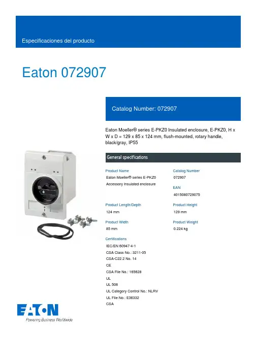
Eaton 072907Eaton Moeller® series E-PKZ0 Insulated enclosure, E-PKZ0, H x W x D = 129 x 85 x 124 mm, flush-mounted, rotary handle, black/gray, IP55General specificationsEaton Moeller® series E-PKZ0 Accessory Insulated enclosure0729074015080729075124 mm 129 mm 85 mm 0.224 kgIEC/EN 60947-4-1 CSA Class No.: 3211-05 CSA-C22.2 No. 14 CECSA File No.: 165628 UL UL 508UL Category Control No.: NLRV UL File No.: E36332 CSAProduct NameCatalog Number EANProduct Length/Depth Product Height Product Width Product Weight Certifications0 AAccessoriesIs the panel builder's responsibility. The specifications for the switchgear must be observed.0 W0 WMeets the product standard's requirements.Is the panel builder's responsibility. The specifications for the switchgear must be observed.Does not apply, since the entire switchgear needs to be evaluated.Meets the product standard's requirements.Black-gray rotary knobPE(N) terminalNEMA 1NEMA 12IP55NEMA 3RMeets the product standard's requirements.Meets the product standard's requirements.Is the panel builder's responsibility.eaton-manual-motor-starters-mounting-e-pkz0-accessory-dimensions.eps eaton-manual-motor-starters-enclosure-e-pkz0-accessory-dimensions-002.epseaton-manual-motor-starters-enclosure-e-pkz0-accessory-dimensions-003.epseaton-manual-motor-starters-enclosure-e-pkz0-accessory-dimensions.eps eaton-manual-motor-starters-enclosure-e-pkz0-accessory-3d-drawing-003.epsDA-CE-ETN.E-PKZ0-GIL03402029ZDA-CD-e_pkz0_gDA-CS-e_pkz0_gRated operational current for specified heat dissipation (In) Product category10.11 Short-circuit ratingEquipment heat dissipation, current-dependent PvidHeat dissipation capacity Pdiss10.4 Clearances and creepage distances10.12 Electromagnetic compatibility10.2.5 Lifting10.2.3.1 Verification of thermal stability of enclosuresFitted with:Degree of protection (front side)10.2.3.2 Verification of resistance of insulating materials to normal heat10.2.3.3 Resist. of insul. mat. to abnormal heat/fire by internal elect. effects10.8 Connections for external conductors10.9.2 Power-frequency electric strength DibujoseCAD model Instrucciones de instalación mCAD modelIs the panel builder's responsibility.Degree of protectionIP55NEMA OtherAmbient operating temperature - max40 °C10.7 Internal electrical circuits and connectionsIs the panel builder's responsibility.10.10 Temperature riseThe panel builder is responsible for the temperature rise calculation. Eaton will provide heat dissipation data for the devices.Static heat dissipation, non-current-dependent Pvs0 W10.9.3 Impulse withstand voltageIs the panel builder's responsibility.Enclosure materialPlasticAmbient operating temperature - min-25 °C10.2.2 Corrosion resistanceMeets the product standard's requirements.10.6 Incorporation of switching devices and componentsDoes not apply, since the entire switchgear needs to be evaluated.10.2.4 Resistance to ultra-violet (UV) radiationPlease enquire10.2.7 InscriptionsMeets the product standard's requirements.10.5 Protection against electric shockDoes not apply, since the entire switchgear needs to be evaluated.ModelBuilt-in10.13 Mechanical functionThe device meets the requirements, provided the information in the instruction leaflet (IL) is observed.10.2.6 Mechanical impactDoes not apply, since the entire switchgear needs to beEaton Corporation plc Eaton House30 Pembroke Road Dublin 4, Ireland © 2023 Eaton. Todos los derechos reservados. Eaton is a registered trademark.All other trademarks areproperty of their respectiveowners./socialmediaevaluated.Is the panel builder's responsibility.Does not apply, since the entire switchgear needs to be evaluated.0 W10.9.4 Testing of enclosures made of insulating material 10.3 Degree of protection of assembliesHeat dissipation per pole, current-dependent Pvid。
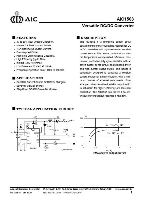
AIC1563Versatile DC/DC Converter FEATURES3V to 30V Input Voltage Operation.Internal 2A Peak Current Switch.1.5A Continuous Output Current.Bootstrapped Driver.High Side Current Sense Capability.High Efficiency (up to 90%).Internal ±2% Reference.Low Quiescent Current at 1.6mA.Frequency Operation from 100Hz to 100KHz.APPLICATIONSConstant Current Source for Battery Chargers.Saver for Cellular phones.Step-Down DC-DC Converter Module.DESCRIPTIONThe AIC1563 is a monolithic control circuitcontaining the primary functions required for DCto DC converters and highside-sensed constantcurrent source. The device consists of an inter-nal temperature compensated reference, com-parator, controlled duty cycle oscillator with anactive current sense circuit, bootstrapped driver,and high current output switch. This device isspecifically designed to construct a constantcurrent source for battery chargers with a mini-mum number of external components. Boot-strapped driver can drive the NPN output switchto saturation for higher efficiency and less heatdissipation. The AIC1563 can deliver 1.5A con-tinuous current without requiring a heat sink. TYPICAL APPLICATION CIRCUITVIN(%)Io (A)00.51 1.52708090100Efficiency vs Output CurrentABSOLUTE MAXIMUM RATINGSSupply Voltage ..............................................................……………............................. 30V Comparator Input Voltage Range ............................................………….......... -0.3V~30V Switch Collector Voltage ....................................................……………......................... 30V Switch Emitter Voltage ......................................................……………......................... 30V Switch Collector to Emitter Voltage ..................................…………............................. 30V Driver Collector Voltage ....................................................…………….......................... 30V Switch Current ................................................………………......................................... 2A Power Dissipation and Thermal CharacteristicsDIP PackageTa= 25°C ............................…………................................ 1.0W Thermal Resistance .............…………......................... 100°C/WSO PackageTa= 25°C ......................……………............................... 625mW Thermal Resistance ...................………...................... 160°C/WOperating Junction Temperature .....................................................………............. 125°COperating Ambient Temperature Range.......................……………......................... 0~70°CStorage Temperature Range ...................................………….................... - 65°C ~ 150°CTEST CIRCUITR1CT2V/0V I DISCHG / IELECTRICAL CHARACTERISTICS(VCC= 5V, Ta=25°C, unless otherwise specified.) PARAMETER TEST CONDITIONS SYMBOL MIN.TYP.MAX.UNIT OscillatorCharging Current 5.0V≤VCC≤30V I CHG102540µA Discharge Current 5.0V≤VCC≤30V I DISCHG100150200µA Voltage Swing PIN 3V OSC0.6V Discharge to Charge Cur-rent RatioV IS =VCC I DISCHG / I CHG 6.0 Current Limit Sense Voltage I CHG=I DISCHG VCC - V IS250300350mV Output SwitchSaturation Voltage, Emitter Follower Connection I DE=1.0A;V BOOST =V DC = VCCV CE(SAT) 1.5 1.8VSaturation Voltage I DC=1.0A; I BOOST=50mA, (Forced β≅20)V CE (SAT)0.40.7V DC Current Gain I SC =1.0A; V CE=5.0V h FE35120Collector Off-State Current V CE=30V I C(OFF)10nA ComparactorThreshold Voltage Ta=25°C0°C ≤ Ta ≤ 70°C V FB 1.2251.211.25 1.2751.29VVThreshold Voltage LineRegulation3.0V≤VCC≤30V REG LINE0.10.3mV/V Input Bias Current V IN=0V I IB0.41µASupply Current V IS =VCC, pin 5>V FB5.0V≤ VCC ≤30VC T=1nFPIN 2=GNDRemaining pins openI CC 1.63mATYPICAL PERFORMANCE CHARACTERISTICSCT, Oscillator Timing Capacitor (nF)t O N -O F F , O u t p u t S w i t c h O N -O F F T i m e (µS )Output Switch ON-OFF Time vs Oscillator TimingCapacitorStandby Supply Current vs Supply VoltageVCC, Supply Voltage (V)I C C , S u p p l y C u r r e n t(m A )1015200.40.81.21.62V F B , T h r e s h o l d V o l t a g e (V )Temperature (°C)V FB , Threshold Voltage vs Temperature1.21.221.241.261.281.301020304050607080V F B , T h r e s h o l d V o l t a g e (m V )Temperature (°C)I S Threshold Voltage vs Temperature250260270280290300310320330340350Emmiter Follower Configuration Output SwitchSaturation Voltage vs Emmiter CurrentI E , Emitter Current (A)1.21.31.41.51.61.71.8V C E (S A T ), S a t u ra t i o n V o l t a g e (V )0.51 1.5Common Emitter Configuration Output Switch Saturation Voltage vs Collector CurrentI C , Collector Current (A)V C E (S A T ), S a t u r a t i o n V ol t a g e (V )0.511.5AIC1563BLOCK DIAGRAMGNDPIN DESCRIPTIONSPIN 1:DC -2A switch collector.PIN 2:DE -Darlington switch emitter.PIN 3:CF-Oscillator timing capacitor.PIN 4:GND -Power ground.PIN 5:FB -Feedback comparator inverting input.PIN 6:VCC -Power supply input.PIN 7:IS-Highside current sense input.VCC - V IS =300mV.PIN 8:BOOST-Bootstrapped driver collector.APPLICATION INFORMATIONSV SAT=Saturation voltage of the output switch.V F=Forward voltage of the ringback rectifier The following power supply characteristics must be chosen:V IN -Nominal input voltage.V OUT -Desired output voltage,V OUT = 1.25 (1 + RB/RA)I OUT -Desired output current.F MIN-Minimum desired switching frequency atselected values for V IN and I OUT.V RIPPLE (P-P) -Desired peak-to-peak output ripple volt-age. In practice, the calculated value willneed to be increased due to the capacitorequivalent series resistance and boardlayout. The ripple voltage should be keptto a low value since it will directly affectthe line and load regulation.A PPLICATION EXAMPLESV INFig. 1 Simplified Battery Charge Circuit for Ni-Cd/ Ni-MH Battery∆T/∆t=1°C/min.Fig. 2 Battery Charge Circuit for Fluctuating Charging Current ApplicationsAPPLICATION EXAMPLES (CONTINUED)Line Regulation V IN = 10V~20V @ I O =1A 40mV Load Regulation V IN = 15V, @ I O =100mA~1A20mV Short Circuit CurrentV IN =15V, @ R L = 0.1Ω1.3AFig. 3 Step-Down ConverterC3Fig. 4 Step-Down Converter with External 5V BootstrapAPPLICATION EXAMPLES (CONTINUED)V OUT Line Regulation V IN = 8V~16V @ I O=200mA100mVLoad Regulation V IN = 12V, @ I O=80mA~200mA40mVFig. 5 Step-Up ConverterFig. 6 Step-Up Converter with External NPN SwitchAPPLICATION EXAMPLES(CONTINUED)IN4.5V~6VLine Regulation V IN = 4.5V~6V @ I O=100mA20mVLoad Regulation V IN = 5V, @ I O=10mA~100mA100mVFig.7 Inverting ConverterPHYSICAL DIMENSIONS8 LEAD PLASTIC SO (unit: mm)SYMBOL MIN MAXA 1.35 1.75A10.100.25B0.330.51C0.190.25D 4.80 5.00E 3.80 4.00e 1.27(TYP)H 5.80 6.20L0.40 1.278 LEAD PLASTIC DIP (unit: mm)SYMBOL MIN MAX A10.381—A2 2.92 4.96b 0.350.56C0.200.36D 9.0110.16E7.628.26E1 6.097.12e 2.54 (TYP)eB —10.92L2.923.81。
BL0972交/直流电能计量芯片数据手册V1.0目录1、产品简述 (5)2、基本特征 (6)2.1主要特点 (6)2.2系统框图 (7)2.3管脚排列(TSSOP20) (7)2.4性能指标 (8)2.4.1电参数性能指标 (8)2.4.2极限范围 (9)3、工作原理 (10)3.1电流电压波形产生原理 (10)3.1.1PGA增益调整 (10)3.1.2相位补偿 (11)3.1.3通道偏置校正 (11)3.1.4通道增益校正 (12)3.1.5电流电压波形输出 (12)3.2有功功率计算原理 (13)3.2.1有功波形的选择 (14)3.2.2有功功率输出 (14)3.2.3有功功率校准 (14)3.2.4有功功率的防潜动 (15)3.2.5有功功率小信号补偿 (15)3.3有功能量计量原理 (16)3.3.1有功能量输出 (16)3.3.2有功能量输出选择 (16)3.3.3有功能量输出比例 (17)3.4电流电压有效值计算原理 (17)3.4.1有效值输出 (18)3.4.2有效值输入信号的设置 (18)3.4.3有效值刷新率的设置 (18)3.4.4电流电压有效值校准 (19)3.4.5有效值的防潜动 (19)3.5快速有效值检测原理 (20)3.5.1快速有效值输出 (20)3.5.2快速有效值输入选择 (21)3.5.3快速有效值累计时间和阈值 (21)3.5.4电网频率选择 (21)3.5.5快速有效值超限数据保存 (22)3.5.6过流指示 (22)3.5.7继电器控制 (22)3.6温度计量 (23)3.7.1线周期计量 (23)3.7.2线频率计量 (23)3.7.3相角计算 (24)3.7.4功率符号位 (24)3.8故障检测 (25)3.8.1过零检测 (25)3.8.2峰值超限 (25)3.8.3线电压跌落 (26)3.8.4过零超时 (27)3.8.5电源供电指示 (28)4、内部寄存器 (30)4.1电参量寄存器(只读) (30)4.2校表寄存器(外部写) (30)4.3OTP寄存器 (32)4.4模式寄存器 (33)4.4.1 MODE1寄存器 (33)4.4.2 MODE2寄存器 (33)4.4.3 MODE3寄存器 (34)4.5中断状态寄存器 (34)4.5.1 STATUS1寄存器 (34)4.5.2 STATUS3寄存器 (34)4.6校表寄存器详细说明 (34)4.6.1 通道PGA增益调整寄存器 (34)4.6.2 相位校正寄存器 (35)4.6.3 有效值增益调整寄存器 (35)4.6.4 有效值偏置校正寄存器 (36)4.6.5 有功小信号补偿寄存器 (36)4.6.7 防潜动阈值寄存器 (36)4.6.8 快速有效值相关设置寄存器 (37)4.6.9 过流报警及控制 (38)4.6.11 能量读后清零设置寄存器 (39)4.6.12 用户写保护设置寄存器 (39)4.6.13 软复位寄存器 (39)4.6.14 通道增益调整寄存器 (40)4.6.15 通道偏置调整寄存器 (40)4.6.16 有功功率增益调整寄存器 (40)4.6.17 有功功率偏置调整寄存器 (41)4.6.20 CF缩放比例寄存器 (41)4.7电参数寄存器详细说明 (42)4.7.1 波形寄存器 (42)4.7.2 有效值寄存器 (42)4.7.3 快速有效值寄存器 (42)4.7.7 电能脉冲计数寄存器 (43)4.7.8 波形夹角寄存器 (44)4.7.9 快速有效值保持寄存器 (44)4.7.11 线电压频率寄存器 (44)5、SPI通讯接口 (45)5.1概述 (45)5.2工作模式 (45)5.3帧结构 (45)5.4读出操作时序 (46)5.5写入操作时序 (47)5.6SPI接口的容错机制 (48)6、典型应用图 (49)7、封装信息 (50)1、产品简述BL0972是一颗内置时钟的单相交/直流电能计量芯片。
aic8800dc参数一、概述AIC8800DC是一款高性能的图像处理芯片,广泛应用于图像采集、处理、传输等领域。
它具有高速的数据处理能力、低功耗、低成本等优点,是许多图像相关应用的理想选择。
二、主要参数1.分辨率:AIC8800DC支持多种分辨率,如VGA(640x480)、XGA (1024x768)等,可根据实际需求进行选择。
2.帧率:AIC8800DC可以以高帧率进行图像采集和处理,适用于需要实时图像传输的应用场景。
3.数据接口:AIC8800DC支持多种数据接口,如HDMI、VGA、CSI 等,方便与各种设备进行连接。
4.像素格式:AIC8800DC支持RGB、YCbCr等多种像素格式,可根据应用需求进行选择。
5.存储器接口:AIC8800DC支持SD卡、内部存储器等存储器接口,方便数据的存储和读取。
6.工作电压:AIC8800DC需要特定的工作电压进行工作,请根据实际需求选择合适的电压范围。
7.工作温度:AIC8800DC可在-40℃至+85℃的温度范围内正常工作。
三、技术特点1.高性能:AIC8800DC具有高速的数据处理能力,可以快速地进行图像采集、压缩、传输等操作。
这种高性能的特性使得AIC8800DC 在许多需要快速图像处理的场景中得到广泛应用。
2.低功耗:AIC8800DC具有低功耗特性,适合长时间工作的应用场景。
这有助于延长设备的使用寿命,节约能源。
3.集成度高:AIC8800DC集成了多种功能,如图像采集、压缩、传输等,大大降低了系统的复杂度。
这使得它成为许多嵌入式系统的理想选择。
4.易于集成:AIC8800DC支持多种软件开发工具和平台,如C/C++、OpenCV等,这使得它更容易与其他系统进行集成。
四、应用领域AIC8800DC适用于各种需要图像处理和传输的应用领域,如安防监控、医疗影像、智能交通、机器人视觉等。
在这些领域中,AIC8800DC的高性能、低功耗、低成本等特性得到了充分的发挥。
500mA Low Dropout Linear RegulatorFEATURESLow Dropout Voltage of 650mV at 500mA Output Current (3V Output Version). Guaranteed 500mA Output Current. Maximum Input Voltage is 8V Low Ground Current at 65µA.2% Accuracy Output Voltage of 1.8V/ 2.0V/2.5V /2.7V/ 3.0V/ 3.3V/ 3.5V/ 3.7V/ 3.8V/ 5.0V/ 5.2V.Only needs 4.7µF Output Capacitor for Stability.Current and Thermal Limiting.APPLICATIONSCD-ROM Drivers. LAN Cards. Microprocessor. RAM Module.Wireless Communication Systems.Battery Powered Systems.DESCRIPTIONThe AIC1723A is a 3-pin low dropout linearregulator. The superior characteristics of the AIC1723A include zero base current loss, very low dropout voltage, and 2% accuracy output voltage. Typical ground current remains approximately 65µA, for loading ranging from zero to maximum. Dropout voltage turns substantially low when output current is 500mA. Built-in output current limiting and thermal limiting provide maximal protection to the AIC1723A against fault conditions.The AIC1723A is available with popular SOT-23, SOT-223, SOT-89 and TO-252 packages.TYPICAL APPLICATION CIRCUITLow Dropout Linear Regulator(C IN and C OUT are electrolytic capacitor)Packing TypeAIC1723A-18PYTR1.8V Version, in SOT-223 Lead Free Package & Tape& Reel Packing TypeSOT-23 MARKINGPart No. CU PU Part No. CU PU AIC1723A-18XU BT18 BT18P AIC1723A-35XU BT35 BT35P AIC1723A-20XU BT20 BT20P AIC1723A-37XU BT37 BT37P AIC1723A-25XU BT25 BT25P AIC1723A-38XU BT38 BT38P AIC1723A-27XU BT27 BT27P AIC1723A-50XU BT50 BT50P AIC1723A-30XU BT30 BT30P AIC1723A-52XU BT52 BT52P AIC1723A-33XU BT33 BT33PSOT-89 MARKINGPart No. CX PX Part No. CX PXAIC1723A-18XX AV18 AV18P AIC1723A-35XX AV35 AV35PAIC1723A-20XX AV20 AV20P AIC1723A-37XX AV37 AV37PAIC1723A-25XX AV25 AV25P AIC1723A-38XX AV38 AV38PAIC1723A-27XX AV27 AV27P AIC1723A-50XX AV50 AV50PAIC1723A-30XX AV30 AV30P AIC1723A-52XX AV52 AV52PAIC1723A-33CY AV33 AV33PSOT-223 MARKINGPart No. CY PY Part No. CY PYAIC1723A-18XY BU18 BU18P AIC1723A-35XY BU35 BU35PAIC1723A-20XY BU20 BU20P AIC1723A-37XY BU37 BU37PAIC1723A-25XY BU25 BU25P AIC1723A-38XY BU38 BU38PAIC1723A-27XY BU27 BU27P AIC1723A-50XY BU50 BU50PAIC1723A-30XY BU30 BU30P AIC1723A-52XY BU52 BU52PAIC1723A-33XY BU33 BU33PABSOLUTE MAXIMUM RATINGSInput Supply Voltage ...................................................…………..…….................. -0.3~8VOperating Temperature Range …………….....………........…………................-40°C~ 85°CJunction Temperature ……………………………………………………………………... 125°CStorage Temperature Range ....................……......................………............. -65°C~150°CLead Temperature (Soldering. 10sec) …………………………………………………… 260°CThermal Resistance Junction to Ambient SOT-23 Package ...….………..… 180°C/W(Assume no Ambient Airflow, no Heatsink) TO-252 Package ...….………..… 100°C/W...….………..… 160°C/W SOT-89PackagePackage...….………..… 155°C/W SOT-223Absolute Maximum Rating are those value beyond which the life of a device may be impaired.TEST CIRCUITRefer to the TYPICAL APPLICATION CIRCUITELECTRICAL CHARACTERISTICS (T A =25°C, C IN =1µF, C OUT =4.7µF, unlessotherwise specified.) (Note 1)PARAMETERTEST CONDITIONSMIN.TYP.MAX. UNITNo LoadOutput Voltage AIC1723A-52 AIC1723A-50 AIC1723A-38 AIC1723A-37 AIC1723A-35 AIC1723A-33 AIC1723A-30AIC1723A-27 AIC1723A-25 AIC1723A-20 AIC1723A-18V IN =8V-2+2 %Line Regulation I L =1mA, 1.8V ≤V OUT ≤3.2V 3.3V ≤V OUT ≤5.2V V IN =4V~8V V IN =5.5V~8V 3 310 15mV Load Regulation (Note 2) I L =0.1~500mA 1.8V ≤V OUT ≤3.9V4.0V ≤V OUT ≤5.2VV IN =5V V IN =7V 10 20 30 50 mV Current Limit(Note 3)V IN =7V, V OUT =0V 500 mADropout Voltage(Note 4)I L =500mA 4.0V ≤V OUT ≤5.2V3.0V ≤V OUT ≤3.9V 2.5V ≤V OUT ≤2.9V 2.0V ≤V OUT ≤2.4V 1.8V ≤V OUT ≤1.9V510 65078011001400 mV Ground Current I O =0.1mA~I MAX 1.8V ≤V OUT ≤3.9V 4.0V ≤V OUT ≤5.2V V IN =5~8V V IN =7~8V 65 659090µANote 1: Specifications are production tested at T A =25°C. Specifications over the -40°C to 85°C operating temperature range are assured by design, characterization and correlation with Statistical Quality Controls (SQC).Note 2:Regulation is measured at constant junction temperature, using pulse testing with a low ON time. Note 3: Current limit is measured by pulsing a short time.Note 4:Dropout voltage is defined as the input to output differential at which the output voltage drops 100mV below the value measured with a 1V differential.TYPICAL PERFORMANCE CHARACTERISTICS0 50100150200250300350400450V DROP vs. I LOADV D R O P (m V )I LOAD (mA)0V DROP vs. I LOADV D R O P (m V )I LOAD (mA)300320340360380400420440V DROP vs. TemperatureV D R O P (m V )Temperature (°C)-40-30-20-1001020304050607080-40-2020406080V DROP vs. TemperatureV D R O P (m V )Temperature (°C)0102030405060Ground Current vs. V ING r o u n d C u r r e n t (µA )V IN (V)Ground Current vs. V ING r o u n d C u r r e n t (µA )V IN (V)TYPICAL PERFORMANCE CHARACTERISTICS (Continued)Ground Current vs. TemperatureG r o u n d C u r r e n t (µA )Temperature (°C)Current Limit vs. TemperatureC u r r e n t L i m i t (m A )Temperature (°C)V OUT vs. TemperatureV O U T (V )Temperature (°C)V OUT vs. TemperatureV O U T (V )Temperature (°C)BLOCK DIAGRAMGNDVOUTVINPIN DESCRIPTIONSVOUT PIN - Output pin. GND PIN - Power GND. VIN PIN - Power Supply Input.PHYSICAL DIMENSIONS (unit: mm)SOT-23 (CU) (PU)SYMBOL MIN MAXA 0.95 1.45 A1 0.05 0.15 A2 0.90 1.30b 0.30 0.50c 0.08 0.22 D 2.80 3.00 E 2.60 3.00 E1 1.50 1.70 e 0.95 BSCe1 1.90 BSC L 0.30 0.60 L1 0.60 REFθ 0˚ 8˚TO-252 (CE) (PE)SYMBOL MIN MAXA 2.19 2.38A1 0.00 0.13b 0.64 0.89b3 5.21 5.46c 0.46 0.61c2 0.46 0.58D 5.33 6.22E 6.35 6.73e 2.28BSCH 9.40 10.41L 1.40 1.78 L1 2.67REF L2 0.51BSC L3 0.89 2.03L4 0.641.02θ0°8°SOT-89 (CX) (PX)SYMBOL MIN MAXA 1.40 1.60B 0.44 0.56B1 0.36 0.48C 0.35 0.44D 4.40 4.60D1 1.50 1.83E 2.29 2.60e 1.50BSCe1 3.00BSCH 3.94 4.25L 0.89 1.20SOT-223 (CY) (PY)SYMBOL MIN MAXA - 1.80A1 0.02 0.10A2 1.55 1.65b 0.66 0.84b2 2.90 3.10c 0.23 0.33D 6.30 6.70E 6.70 7.30E1 3.30 3.70e 2.30BSC e1 4.60BSC L 0.90 -θ0°8°Note:Information provided by AIC is believed to be accurate and reliable. However, we cannot assume responsibility for use of any circuitry other than circuitry entirely embodied in an AIC product; nor for any infringement of patents or other rights of third parties that may result from its use. We reserve the right to change the circuitry and specifications without notice.Life Support Policy: AIC does not authorize any AIC product for use in life support devices and/or systems. Life support devices or systems are devices or systems which, (I) are intended for surgical implant into the body or (ii) support or sustain life, and whose failure to perform, when properly used in accordance with instructions for use provided in the labeling, can be reasonably expected to result in a significant injury to the user.。
有关存储式行程检测参数#7 #6 #5 #4 #3 #2 #1 #01300[数据形式] 位型OUT 用参数(N0.1322,N0.1323)设定的存储式行程检测2的区域为0:禁止内侧区域 l :禁止外侧区域LMS 存储式行程检测切换信号EXLM 是否有效O :无效 l :有效注:存储式行程检测1具有2组设定禁止区域的参数。
用存储式行程限位切换信号。
可以选择哪组设定的禁止区域有效。
1)禁止区域I :参数No .1320。
No .1321 2)禁止区域ll :参数No .1326。
No .1327 RL3行程检测3释放信号RLSOT3足否有效0:有效 l :无效LZR 接通电源后到手动回参考点之前,是否进行存储式行程检测0:进行 l :不进行注:使用绝对位置编码器的情况下,接通电源时,参考点已经建立。
因此与设定无关,接通电源后。
可直接进行存储式行程检测。
BFA 当发出超出存储式行程检测的指令时 0:在超出行程检测后出现报警 l :在超出行程检测之前出现报警注:刀具在离边界最大F /7500(mm)之前或超出边界后停止。
(F :到达边界时的进给速度(单位:mm ,min )#7 #6 #5 #4 #3 #2 #1 #01320数据形式 位轴型OT2x 每个轴是否进行存储式行程检测2的检查。
0:不进行 l :进行OT3x 每个轴是否进行存储式行程检测3的检查0:不进行 l :进行1320 各轴存储式行程检测1的正方向边界的座标值 1321各轴存储式行程检测1的负方向边界的座标值 [数据形式] 双字轴型 [数据单位][数据范围] -99999999~99999999在机械座标系上,分别设定各轴存储行程检测1的正方向及负方向的边界座标值。
设定的边界的外侧为禁止刀具进入的领域。
在参数NO.1320上设定+方向边界的机械座标值Xp、yp、Zp;在参数N0.1321上设定一方向边界的机械座标值 Xm、Ym、Zm。
Boeing C-17 Transport2 EATON Aerospace C5-14G April 2014Eaton is a recognized leader in the aerospace industry and is a key supplier of hydraulics, fuel, conveyance and actuation products on the C-17. With this cutting edge technology, Eaton provides a broad array ofproducts including a 4000 psi quad-redundant hydraulic system. Two of four systems are connected using a reversible motorpump, in case ofemergency shutdown of any engine. All four systems incorpo-rate a primary and secondary engine-driven pump, part of Eaton's Vickers ® product line, ensuring a constant supply of hydraulic power during all phases of flight. Underemergency conditions, hydraulic power is generated by a ram air turbine (RAT) pump, which is deployed automatically and drives an Eaton pump.The C-17's unique capability to land on short runways is assisted by Eaton's pitch trim motors. The pitch trim motors position the horizontal stabilizer during the short landings and takeoffs for optimal performance.The C-17 hydraulic system incor-porates main engine and AC motor-driven pumps as well as pitch trim and OBIGGS drive motors. Eaton also provides additional system hydraulic and pneumatic units. These include servo control valves, a brake pressure metering valve, winch modules and a cargo AirDelivery System (ADS) control manifold. Electrical equipment provided by Eaton includes the Auxilary Power Unit (APU) air inlet actuator, ramp lock, logistic rail locks and RAT release actuator.The C-17 is also equipped with Eaton fluid health monitoring technology. The magnetic chip collectors, electro-optic and float activated sensors and system check valves are on allsecondary power systems. These products are primarily used to monitor harmfulmaterials in the flow of hydraulic and lube fluids during the run time of the aircraft.Other products on the C-17 include Eaton’s Aeroquip ®product line of quick disconnect couplings and self sealing “B”nut fittings and hose products, including high pressure Kevlar ® hoses. In addition, Eaton provides thepylon-mounted main fuel line for each engine, incorporating two quick disconnects into a convo-luted hose joined with a complex bent tube.Eaton also provides fuel boost pumps and canisters which were specifically designed for the C-17. They were designed and manufactured to provide excellent pumping performance at high climb rates and altitudes with many different types of fuel. To enhance fire safety, Eaton also provides the aircraft mounted valves that control the flow of nitrogen gas from the OBIGGS system to the fuel tanks.The United States Air Force Boeing C-17 Globemaster III is a high-wing, four-engine, T-tailed aircraft with a rear-loading ramp. It is 174 feet in length, has a height of 55.08 feet and a wingspan of 169.75 feet. Maximum takeoff gross weight is 585,000 lbs; maximum payload is 164,900 lbs. It was designed to expand the capability of the AirMobility Command (AMC) by enabling the long distance transport of troops and heavy combat equipment directly to small austere landing sites. The austere landing site capability of the aircraft is further enhanced by having all systems fully independent of ground support equipment.The Boeing C-17 alsoembodies Short T akeoff and Landing (STOL) technology. The unique ability to land cargo on very short airstrips and then take off again is achieved through theutilization of propulsive lift aerodynamics and advanced composite structures for lighter weight.The aircraft is powered by four Pratt & Whitney PW2040 series (Boeing 757 Derivative) turbofan engines, designated by the Air Force as F117 PW-100, each producing 40,440 lbs of thrust, located on pylons ahead of andbelow the wing leading edge. Engine thrust is blown through the fully extended flaps to create additional lift. This feature is useful in short takeoff and landings, and in low speed maneuvers. The engines are also equipped with directed-flow thrust reversers capable of deploy-ment in flight. On theground, a fully loaded aircraft using engine thrust reversers, can back up a 2% slope.Boeing C-17 Component and Systems OverviewEaton’s Aerospace Product Capabilitiesmponent and Systems OverviewEATON Aerospace C5-14G April 2014 31234567891011121314151617181920212324252627282930313940412232333435363738Eaton’s Boeing C-17 Systems Components6.OBIGGS LP Valve7.OBIGGS Compressor Motor8.OBIGGS II Super Joint Assembly9.OBIGGS HP Valve 10.Fuel Boost Pump11.Fuel Crossfeed Gate Valve 12.Float Activated Level Sensors 13.Main Fuel Line14.Low Flow Shutoff Valve 15.Breathers16.Engine-Driven Pumps 17.Dual Brake Metering Valves 18.AC Motorpump19.Fluid Conveyance Line Assembly 20.RAT Pump21.RAT Release Actuator22.Steering & Bypass Control Valves 23.Pitch Trim Motors24.Variable Restraint Assembly 25.Gate Release Assembly26.Ramp Lock Actuator 27.Winch Control Module 28.Cargo Rail Actuator29.Cable Tension Arm Assembly 30.Flap/Slat Position Transmitter 31.APU Air Inlet Actuator 32.Aft/Flap Slat Module33.Ratio Changer Actuator - Aileron Ratio Changer Assembly34.Rudder Cable Control Assembly 35.Aileron Load Feel Assembly 36.Rudder Load Feel Assembly 37.Trim Actuator Control,Elevator Load Feel Assembly38.Control Stick Rudder Pedal Assembly, Park Brake Mechanism39.Cargo Air Delivery Manifold 40.Stabilzation Strut System 41.Levelmaster ®1.Magnetic Chip Collectors2.Differential Pressure Switch3.Hydraulic Pressure Switch4.Mainshaft Carbon Seals5.Gear Box Seals4 EATON Aerospace C5-14G April 2014145/155 Series Soft Seal Ground Support CouplingsEaton's 145/155 series couplings have been the industry standard for ground service applications for over 50 years. During this time the design has been continuously improved to increase reliability, safety and ease of operation. Improvements have been made to include elastomeric soft seals in both the aircraft half and ground cart half to virtually eliminate fluid spillage and air inclusion during operation, and blunt start threadsto prevent cross threading.Main Fuel Line Eaton's main fuel line provides fuelfrom the engine pylon to the engine fuel pumps on each C-17 engine. The product features 2-in diameter convoluted T eflon ® hoses, covered with slip-on silicon fire protection sleeves, and integrally mated with two quick disconnect coupling halves and a complex bent tube. The convoluted hose combines the routing flexibility of lightweight rubber hose with the temperature range and fluid compatibility of T eflon. The assembly can be disconnected from the pylon withno fuel spillage.1817 Low Profile Ball Bearing Plane Swivel JointsRotational movement in the landing gear hydraulic system of the C-17 is supplied by Eaton 1817 series low profile ball bearing plane swivel joints. The 1817 series was designed and qualified to MIL-J-5513 for low torque, high side load applications.Flexible Hose Assemblies Eaton's hose assemblies are utilized extensively throughout the C-17 aircraft. The assemblies can be found in the hydraulic system, the oxygen system, the fuel system and lube oil system. Eaton provides lightweightNomex braided, convoluted hose assemblies to AS1227. Kevlarreinforced T eflon ® hoses toAS4623 are used in the 4,000-psi (27579 kPa) hydraulic system offering a significant weightsavings over more traditional wire reinforced hose assemblies.Low Profile, Self-Sealing Hydraulic "B" Nut Fittings Eaton's low profile, self-sealing hydraulic "B" nut fittings, offer a small envelope size with minimal weight. The "B" nut design is for both 4,000 psi high pressure and low pressure hydraulic systems used on the Boeing C-17.OBIGGS II Flex-CouplingAssemblyEaton provides its flex-coupling assembly that supports the second generation on-board inert gas generator system that replaces gas bottles used in older generation aircraft and replaces a first generation OBIGGS system.Mainshaft SealsMainshaft seals are used along the aircraft engine main shaft, sealing in lubrication of themain bearings.Gearbox SealsGearbox seals are installedin the engine gearbox that contains bearing lubrication which the accessories receive their power. This includes acces-sories that power the ancillary functions around the engine including the starter, fuelcontrols, fuel pumps, hydraulicpumps, and more.Magnetic Chip Collectors The C-17 engine oil system incorporates Eaton’s magnetic chip collectors for the capture of ferrous engine wear debris. These collectors have a self-closing valve which will prevent oil leaks up to 300 psig (20.69 bar), and rare earth magnets foreffective debris capture over long periods of time.System Check ValveThe C-17 integrated drive gener-ator (IDG) contains an Eaton 2C6107 system check valve. This valve has a 10 micron sintered disc for filtering capability, and a flow restrictor that controls air flow through the valve.Float-Activated Level Sensor The 2E6139 float-activated liquid level sensor is located in the C-17 integrated drive generator. The sensor, weighing approxi-mately 30 grams, providesfeedback upon sensing an insuf-ficient fluid level in the IDG.Breather (supplied to Hamilton Sundstrand)Eaton’s breather provides pressure equalization and air filtration for the lubrication circuit for the OBIGGScompressor. The filter element is made of corrosion resistant mono filament material.5 Cargo/Air Delivery System(ADS) Control ManifoldThe cargo/ADS control manifold isdesigned for air drop operationsand on/off loading on the ground.The cargo/ADS control manifoldcontains all valving necessary tocontrol the cylinders in the aerialdelivery system including thecargo ramp, ramp latches, ramptoes, and cargo door actuators.It also controls the cargo doorup and down locks, the left andright drouge parachute and thedeploy mechanisms, and thetow/release and drogue chutejettison mechanism. Themanifold can be operatedelectrically from the forwardloadmaster station, or manuallyfrom the rear station.Winch Control ModuleEaton’s control moduleprovides control of fluid flow tothe hydraulic motor operatedwinch when commanded by theloadmaster. The moduleregulates hydraulic flow inresponse to an electrical inputcommand from the winchcontrol panel.The winch control moduleconsists of a servo valve, reliefvalve across the motor ports,anti-cavitation make up checkvalve and two inlet pressureblocking valves. One is usedfor the winch brake releaseand the other is for control ofthe hydraulic motor dualspeed feature.Dual Brake PressureMetering Valve AssemblyThese valve assemblies areinstalled in the landing gearwheel well and are controlled bythe pilot through a mechanicalclosed loop cable system. Theassembly controls the hydraulicactuation pressures to thebrakes as a function of inputposition from the rudder pedals.Included in the assembly aretwo force command meteringvalves for modulating brakepressure and a despin actuatorto stop the wheels fromspinning upon landing gearretraction.Steering and BypassControl ValvesThe C-17 hydraulic systemincludes a set of nosewheelsteering controls and nosewheelsteering bypass valves. Thebypass valve is used to unloadthe steering actuators duringtowing and allows for centeringof the nose gear while beingstowed. The steering valvereceives a clockwise or counter-clockwise manual input from therudder pedals, and provideshydraulic fluid flow to thenosewheel steering controlactuators. Position feedback tothe valve is achieved through aclosed loop cable system. Thevalves are tandem redundant,dual system with rip stopconstruction between the twohydraulic systems.Pitch T rim Actuator MotorThe C-17 pitch control ismaintained by a rotary actuatorlocated in the aircraft empen-nage. The pitch trim actuatormotor provides positional controlof the horizontal stabilizer. TwoEaton bi-directional inlinehydraulic motors, with adisplacement of .22 cu in/rev(3.60 ml/rev), produce a theoret-ical torque of 137 in-Ibs at3900 psi (26,889 kPa) pressuredifferential. The motor isdesigned to withstand twomillion reverse load cycles, and2000 psi return pressure. TheMF3-022 motor contains anti-cavitation check valves andweighs 6.2 Ibs (2.81 kg).Engine-Driven Hydraulic PumpThe unique design and constructionof Eaton's 4000 psi (27,579 kPa)pumps allow them to operate atrelatively high efficiencies, thusenabling each unit to generatenearly 80 hydraulic horsepower.Additional features of the pumpsinclude an electrical depressuriza-tion valve (EDV), a blocking valve,and an inlet boost impeller. Thepackage also weighs less than28 Ibs dry. (12.25 kg).OBIGGS CompressorDrive MotorThe OBIGGS compressor isdriven by Eaton's inline,constant speed hydraulic motorwhich features integral speedcontrol and an electricallyoperated shut-off valve. When28 VDC is applied to thesolenoid, the motor will rotate,creating a constant speedbetween 2250 and 2550 rpm,over the power range requiredby the compressor output flow.Motor displacement is .598 cuin/rev (9.80 ml/rev). The weightof the OBIGGS drive motor andcontrols is 14.6 Ibs (6.62 kg).AC Motor-Driven PumpEaton provides four .42 cuin/rev (6.88 ml/rev) displacementAC motor-driven pumps peraircraft.The AC motor-driven provideflow to each of the four aircrafthydraulic systems. This allowsthe aircraft to be fully checkedout before flight without theneed of a ground cart. The ACmotor-driven is also used topower the on-board cargoloading system, and to stabilizethe aircraft during loading. Thevariable displacement motor-driven produces up to 10 gpm(37.87 L/min) at 6000 rpm. The3-phase, 200/115 volt, 400 Hzelectric motor is a dry rotor oiljacket cooled design withintegral thermal annunciation.Dry weight of this completeassembly is 42.5 1bs (19.28 kg).EATON Aerospace C5-14G April 20146 EATON AerospaceC5-14G April 2014Gate Release Assembly The Eaton Gate Release Actuator is used on the C-17 aircraft to trip cargo pallet tie-downs during airborne off-loading. Operation of the actuator is electrically controlled by the aircraft loadmaster.A 28 Vdc brush-type motor, directly coupled to a ballscrew, provides the quick retraction stroke required for a clean release of the load. An internal extension spring returns the actuator to the "locked"position after electrical power is removed.Rotary ActuatorEaton's rotary actuator operates the APU air inlet and consists of a reversible DC motor with an electrical brake. The brake isdisengaged when electric power is applied to the motor, and engaged when power is off, preventing the output shaft from being back driven.Rotation of the output shaft is controlled by applying voltage to the CW or CCW fields.Internal limit switches open at the end of the stroke to limit rotation of the outputshaft. Internal mechanical stops limit the travel in the event of an overrun of the electrical limit switchesAileron & Rudder T rim ActuatorEaton's actuator provides a linear output force which operates the slat hydraulic control valve and trims the aileron and rudder control systems on the C-17.The actuator is powered by two redundant DC motors. Four linear variable differential trans-formers (LVDT) are mounted integrally with the actuator housing and provides position feedback to the four flight control computers.A direct gear drive permitsindividual or simultaneous motor operation. Each motor is locked in position by a spring loaded brake. The brake holds the actuator in place and prevents backdriving of the other motor during single motor operation. Mechanical stops limits both extend and retract travel.Rudder Ratio Changer and Door Lock Actuator Eaton’s rudder travel actuator imparts controlled linear motion to change the rudder input to output ratio of the control mechanism. This feature is engaged when part or fullmanual reversion control of the aircraft surfaces is required. In this mode, the mechanicalinputs to the aileron and elevator control valves are changed depending on the authority required. The actuator consists of reduction gears, a screw jack, and attached fittings that are driven by an integral 28 Vdc electric motor. The actuator is capable of having its direction reversed at any intermediate position. Stroke reversal is accomplished by reversing DC voltage polarity to the motor by means of external switching. This function removes power from the motor at each end of the stroke.Fuel Crossfeed Gate Valve Eaton's crossfeed gate valve is a 2-1/2 inch gate valve used to control the transfer of fuel from one tank’s boost pumps toanother tank’s engine. The valve assembly consists of a tank mounted body assembly, amotor operated actuator, and an actuator support assembly. The actuator, gate body, and primary seals are interchangeable and removable without draining the tank. The weight of thecomplete valve assembly is 4.4lbs (2.0 kg).High and Low Pressure Regulating ValvesEaton's aircraft mountedpressure valves control the flow of nitrogen gas from theOnboard Inert Gas Generation System (OBIGGS) to the fuel tanks to enhance fire safety. Pressure regulation reduces the elevated pressure of the stored gas down to the near-atmospheric levels required for the fuel tanks. Each system comprises one High Pressure Regulating Valve (HPRV) and two Low Pressure Regulating Valves (LPRV), each incorporatingshut-off valves.Hydraulic Pressure SwitchThis small, lightweight, extremely reliable hydraulic pressure switch is usedextensively in aerospace and is qualified for both commercial and military applications. These Eaton switches are designed to be used in any fluid that is compatible with stainless steel or aluminum. The pressure switch design incorporates a snap-action electricalmicroswitch which is actuatedby a piston-sensing element.Levelmaster®The C-17 Levelmaster® provides four discrete bits of potable water level information. The assembly consists of fourelectro-optic sensors positioned at customer specified levels of: full, 2/3, 1/3 and empty. As liquid covers each prism point, a light is activated in a panel mounted indicator, providing level status. A press-to-test button on the indicator will energize those lights corresponding to thesensors which are not immersed in liquid.EATON Aerospace C5-14G April 20147Ramp Lock ActuatorEaton's ramp lock actuator provides control of the cargo ramp lock on the aircraft. A helical spring on the actuator helps to overcome flight loads and extends the actuator to release the ramp lock.The actuator is operated by a 28 Vdc motor driving through a two-stage spur gear drive train into a multiplate slip clutch and a ball screw assembly. Motor direction is controlled by electro-mechanical relays that areenergized and de-energized by the aerial delivery system controller. Actuator controlfeedback is provided by external position sensors. The multiplate slip clutch allows the actuator to be overridden in the event that power is lost to the actuator.Cargo Rail ActuatorEaton's cargo rail actuator is used to perform the lock/arm/release function for the cargo pallets constrained by cargo bay logistics and aerial delivery rails on the C-17 aircraft. The actuator is operated by a 115 Vdc, 400 Hz, three-phase motor that drives a reduction gear to a ball screw and output rod. The input gear for the ball screw is located between two pairs of Belleville spring washers, which absorb the peaks of shock loads when the output contacts the mechan-ical stops. The actuator is avail-able with or without a brake on the motor. The manual brake override allows the actuator to be back driven when power is removed.Fuel Boost Pump and Canister Eaton’s fuel boost pump is fitted in a tank mounted canister for ease of installation and to avoid draining the tank when removing the pump.It is specifically designed and manufactured to provide excel-lent pumping performance at high climb rates and altitudes with many different types of fuel. This pump has the ability to provide vapor free fuel, even at near boiling conditions, with hotvolatile fuels.RAT Deployment Actuator Eaton’s RAT actuator is a quick, short stroke device designed to release the latch that holds the ram air turbine in stowed position, on the aircraft.The actuator is operated by a 28 VDC motor splined directly to an acme screw. An acme nut, restrained from rotation by a spline interface with the housing, provides the linear action to position an output rod. An acme screw is held between two pairs of Belleville spring washers in contact with thrust bearings, which absorb peakshock loads when the output rod strikes the mechanical stops.Stabilization Strut System Eaton's stabilization strut system is used to stabilize the aircraft for cargo loading and unloading and to jack up the rear of the aircraft for changing the main landing gear tires. The system consists of four different compo-nents, the stabilization strut, the door deployment actuator, the control manifold, and the isola-tion valve. The control manifold is used to operate the system manually or electronically, and maintains a set pressure in the stabilization strut as cargo is loaded. The door actuator is used to open the strut compart-ment door to deploy the strut.Variable Restraint Assembly Eaton’s rotary actuators are used to adjust the release point on the variable restraint lock mechanisms on the aircraft’s aerial delivery rail.The actuator is powered by a bi-directional 115 VAC single phase motor. The motor has an integral brake which holds the output shaft in position when power is removed. The brake is released upon re-application of power.A film type multi-turn potenti-ometer is connected to the epicyclic gear train and is used to track the number of revolu-tions of the output shaft and displays the load setting at thesidewall control panel.Copyright © 2014 EatonTeflon® is a registered trademark of Dupont. All Rights ReservedForm No. C5-14GApril 2014EatonAerospace Group9650 Jeronimo Road Irvine, California 92618Ph 949 452-9500Fax 949 452-9555/aerospace。
50mA Low Dropout Linear Regulatorn FEATURESl4% Accuracy Output Voltage.l Low Dropout Voltagel Guaranteed 50mA Output Current.l Internal P-MOSFET Draws no Base Current.l Low Ground Current.l Output Voltage of 3.0V/ 3.3V/ 3.6V/ 4.5V/ 5.0V Available.l Input Voltage Range up to 13V.l Needs only 1µF for Stability.n APPLICATIONSl Toys.l Battery Powered Systems.l Audio/Video Systeml Wireless Communication Systems.n DESCRIPTIONT he AIC1727 is a 3-pin low dropout linear regulator. The superior characteristics of the AIC1727 include zero base current loss, low dropout voltage and accurate output voltage.Typical ground current remains approximately 4µA, from no load to maximum loading conditions.T he AIC1727 comes in the popular 3-pin SOT-23, SOT-89, TO-92 packages.n TYPICAL APPLICATION CIRCUITL ow Dropout Linear Regulatorn ORDERING INFORMATION ArrayAIC1727-XXCXXPACKAGING TYPEU: SOT-23X: SOT-89ZT: TO-92ZL: TO-92OUTPUT VOLTAGE30: 3.0V33: 3.3V36: 3.6V45: 4.5V50: 5.0Vn ABSOLUTE MAXIMUM RATINGSI nput Supply Voltage...................................................…………..…….................... -0.3~13VO perating Junction Temperature Range.....………........…………..…..............-40°C~ 85°C S torage Temperature Range ....................……......................……….............. -65°C~150°C P ower Dissipation SOT-89 Package....…...…................. 0.5WTO-92 Package.....…………............. 0.5WSOT-23 Package .....………….......…. 0.35Wn TEST CIRCUITR efer to the TYPICAL APPLICATION CIRCUITn ELECTRICAL CHARACTERISTICS (Ta=25°C, C IN=1F, CƒÝ=1µF, unless otherwiseOUTN ote 1:Guaranteed by design.N ote 2:Regulation is measured at constant junction temperature, using pulse testing with a low ON time.N ote 3:Dropout voltage is defined as the input to output differential at which the output voltage drops 100mV below the value measured with a 1V differential.n TYPICAL PERFORMANCE CHARACTERISTICSV INV O U T4.5V5.5V3.0V I O U T =1mA C OUT =1µF200mV/DIVTime (1mS/DIV)Line Transient ResponseV INV O U T4.5V5.5V3.0V I OUT =10mA C OUT =1µF200mV/DIVTime (1mS/DIV)Line Transient ResponseV INV O U T5.5V7.5V5.0VI OUT =1mA C OUT =1µF200mV/DIVTime (1mS/DIV)Line Transient ResponseV INV O U T6.5V7.5V5.0V I OUT =10mA C OUT =1µF200mV/DIVTime (1mS/DIV)Line Transient ResponseV OUTI OUT10mA5.0V0mAC O U T =1µF200mV/DIVTime (1mS/DIV)Load Transient ResponseV OUTI OUT30mA5.0V0mAC OUT =1µF200mV/DIVTime (1mS/DIV)Load Transient Responsen TYPICAL PERFORMANCE CHARACTERISTICS (Continued)V OUTI OUT50mA5.0V0mAC OUT =1µF200mV/DIVTime (1mS/DIV)Load Transient Response010********20040060080010001200140016001800Dropout Voltage vs Load CurrentD r o p o u t V o l t a g e (m V )Load Current (mA)Ground Current vs VG r o u n d C u r r e n t (µA )V IN (V)2468101214012345G r o u n d C u r r e n t (µA )Temperature (°C)Ground Current vs Temperature-40-20204060800.00.51.01.52.02.53.03.54.04.55.05.56.0Ground Current vs TemperatureG r o u n d C u r r e n t (µA )Temperature (°C)-40-20204060800.00.51.01.52.02.53.03.54.04.55.05.56.0n BLOCK DIAGRAMVINGNDVOUTn PHYSICAL DIMENSIONSl SOT-23 (unit: mm)SYMBOLMIN MAX A 1.00 1.30A1—0.10A20.700.90b 0.350.50C 0.100.25D 2.70 3.10E1.40 1.80e 1.90 (TYP)H 2.60 3.00L0.37—£c 11°9°l SOT-23 MarkingPart No.Marking AIC1727-30CU BJ30AIC1727-33CU BJ33AIC1727-36CU BJ36AIC1727-45CU BJ45AIC1727-50CUBJ50l SOT-89 (unit: mm)SYMBOL MIN MAXA 1.40 1.60B0.360.48C0.350.44D 4.40 4.60D1 1.62 1.83E 2.29 2.60e 1.50 (TYP.)e1 3.00 (TYP.)H 3.94 4.25L0.89 1.20 l TO-92 (unit: mm)SYMBOL MIN MAXA 4.32 5.33C0.38 (TYP.)D 4.40 5.20E 3.17 4.20e1 1.27 (TYP.)L12.7-。