PK55F80中文资料
- 格式:pdf
- 大小:122.59 KB
- 文档页数:2
Features• Low Power Consumption • Industry Standard Size• Industry Standard Pinout • Choice of Character Size7.6 mm (0.30 in), 10 mm (0.40 in), 10.9 mm (0.43 in), 14.2 mm (0.56 in), 20 mm (0.80 in)• Choice of ColorsAlGaAs Red, High Efficiency Red (HER), Yellow, Green• Excellent Appearance Evenly Lighted Segments±50° Viewing Angle• Design FlexibilityCommon Anode or Common CathodeSingle and Dual DigitLeft and Right Hand Decimal Points±1. Overflow Character• Categorized for Luminous IntensityYellow and Green Categorized for ColorUse of Like Categories Yields a Uniform Display• Excellent for Long Digit String Multiplexing DescriptionThese low current seven segment displays are designed for applica-tions requiring low power consumption. They are tested and selected for their excellent low current characteristics to ensure that the segments are matched at low currents. Drive currents as low as 1 mA per segment are available.Pin for pin equivalent displays are also available in a standard current or high light ambient design. The standard current displays are available in all colors and are ideal for most applica-tions. The high light ambient displays are ideal for sunlight ambients or long string lengths. For additional information see the 7.6 mm Micro Bright Seven Segment Displays, 10 mm Seven Segment Displays, 7.6 mm/10.9 mm Seven Segment Displays, 14.2 mm Seven Segment Displays, 20 mm Seven Segment Displays, or High Light Ambient Seven Segment Displays data sheets.Low Current Seven SegmentDisplays Technical Data HDSP-335x SeriesHDSP-555x SeriesHDSP-751x SeriesHDSP-A10x Series HDSP-A80x Series HDSP-A90x Series HDSP-E10x Series HDSP-F10x Series HDSP-G10x Series HDSP-H10x Series HDSP-K12x, K70x Series HDSP-N10x SeriesHDSP-N40x SeriesDevicesAlGaAs HER Yellow Green Package HDSP-HDSP-HDSP-HDSP-Description Drawing A1017511A801A9017.6 mm Common Anode Right Hand Decimal A A1037513A803A9037.6 mm Common Cathode Right Hand Decimal B A1077517A807A9077.6 mm Common Anode ±1. Overflow C A1087518A808A9087.6 mm Common Cathode ±1. Overflow D F10110 mm Common Anode Right Hand Decimal E F10310 mm Common Cathode Right Hand Decimal F F10710 mm Common Anode ±1. Overflow G F10810 mm Common Cathode ±1. Overflow H G10110 mm Two Digit Common Anode Right Hand Decimal X G10310 mm Two Digit Common Cathode Right Hand Decimal Y E100335010.9 mm Common Anode Left Hand Decimal I E101335110.9 mm Common Anode Right Hand Decimal J E103335310.9 mm Common Cathode Right Hand Decimal K E106335610.9 mm Universal ±1. Overflow[1]L H101555114.2 mm Common Anode Right Hand Decimal M H103555314.2 mm Common Cathode Right Hand Decimal N H107555714.2 mm Common Anode ±1. Overflow O H108555814.2 mm Common Cathode ±1. Overflow P K121K70114.2 mm Two Digit Common Anode Right Hand Decimal R K123K70314.2 mm Two Digit Common Cathode Right Hand Decimal S N10020 mm Common Anode Left Hand Decimal Q N101N40120 mm Common Anode Right Hand Decimal T N103N40320 mm Common Cathode Right Hand Decimal U N10520 mm Common Cathode Left Hand Decimal V N106N40620 mm Universal ±1. Overflow[1]W Note:1. Universal pinout brings the anode and cathode of each segment’s LED out to separate pins. See internal diagrams L or W.Part Numbering System5082-x xx x-x x x xxHDSP-x xx x-x x x xxMechanical Options[1]00: No mechanical optionColor Bin Options[1,2]0: No color bin limitationMaximum Intensity Bin[1,2]0: No maximum intensity bin limitationMinimum Intensity Bin[1,2]0: No minimum intensity bin limitationDevice Configuration/Color[1]G: GreenDevice Specific Configuration[1]Refer to respective datasheetPackage[1]Refer to Respective datasheetNotes:1. For codes not listed in the figure above, please refer to the respective datasheet or contact your nearest Agilent representative fordetails.2. Bin options refer to shippable bins for a part-number. Color and Intensity Bins are typically restricted to 1 bin per tube (excep-tions may apply). Please refer to respective datasheet for specific bin limit information.Package DimensionsPackage Dimensions (cont.)Package Dimensions (cont.)*The Side View of package indicates Country of Origin.Package Dimensions (cont.)Package Dimensions (cont.)Package Dimensions (cont.)Internal Circuit DiagramInternal Circuit Diagram (cont.)Absolute Maximum RatingsAlGaAs Red - HDSP-HERA10X/E10X/H10X HDSP-751X/Yellow GreenK12X/N10X/N40X335X/555X/HDSP-A80X HDSP-A90X Description F10X, G10X Series K70X Series Series Series Units Average Power per Segment or DP375264mW Peak Forward Current per 45mA Segment or DPDC Forward Current per15[1]15[2]mA Segment or DPOperating Temperature Range-20 to +100-40 to +100°C Storage Temperature Range -55 to +100°C Reverse Voltage per Segment 3.0V or DPWave Soldering Temperature for 3Seconds (1.60 mm [0.063 in.] below 250°C seating body)Notes:1. Derate above 91°C at 0.53 mA/°C.2. Derate HER/Yellow above 80°C at 0.38 mA/°C and Green above 71°C at 0.31 mA/°C.Electrical/Optical Characteristics at T A = 25°CAlGaAs RedDeviceSeriesHDSP-Parameter Symbol Min.Typ.Max.Units Test Conditions315600I F = 1 mA A10x3600I F = 5 mA330650I F = 1 mAF10x, G10x3900I F = 5 mA390650I F = 1 mA E10x Luminous Intensity/Segment[1,2]I Vµcd(Digit Average)3900I F = 5 mA400700I F = 1 mAH10x, K12x4200I F = 5 mA270590I F = 1 mAN10x, N40x3500I F = 5 mA1.6I F = 1 mAForward Voltage/Segment or DP V F 1.7V I F = 5 mA1.82.2I F = 20 mA PkAll Devices Peak WavelengthλPEAK645nmDominant Wavelength[3]λd637nmReverse Voltage/Segment or DP[4]V R 3.015V I R = 100 µATemperature Coefficient of∆V F/°C-2 mV mV/°CV F/Segment or DPA10x255F10x, G10x320E10x340Thermal Resistance LED RθJ-PIN°C/W/SegH10x, K12x Junction-to-Pin400N10x, N40x430High Efficiency RedDeviceSeriesHDSP-Parameter Symbol Min.Typ.Max.Units Test Conditions160270I F = 2 mA 751x1050I F = 5 mA200300I F = 2 mA Luminous Intensity/Segment[1,2]I V mcd(Digit Average)1200I F = 5 mA335x, 555x,K70x270370I F = 2 mA1480I F = 5 mA1.6I F = 2 mAForward Voltage/Segment or DP V F 1.7V I F = 5 mA2.1 2.5I F = 20 mA Pk All Devices Peak WavelengthλPEAK635nmDominant Wavelength[3]λd626nmReverse Voltage/Segment or DP[4]V R 3.030V I R = 100 µATemperature Coefficient of∆V F/°C-2mV/°CV F/Segment or DP751x200335x Thermal Resistance LED RθJ-PIN280°C/WJunction-to-Pin555x, K70x345YellowDeviceSeriesHDSP-Parameter Symbol Min.Typ.Max.Units Test Conditions Luminous Intensity/Segment[1,2]250420I F = 4 mA(Digit Average)I V mcd1300I F = 10 mA1.7I F = 4 mAForward Voltage/Segment or DP V F 1.8V I F = 5 mA A80x2.1 2.5I F = 20 mA PkPeak WavelengthλPEAK583nmDominant Wavelength[3,5]λd581.5585592.5nmReverse Voltage/Segment or DP[4]V R 3.030V I R = 100 µATemperature Coefficient of∆V F/°C-2mV/°CV F/Segment or DPThermal Resistance LED RθJ-PIN200°C/WJunction-to-PinGreenDeviceSeriesHDSP-Parameter Symbol Min.Typ.Max.Units Test Conditions Luminous Intensity/Segment[1,2]250475I F = 4 mA(Digit Average)I V mcd1500I F = 10 mA1.9I F = 4 mAForward Voltage/Segment or DP V F 2.0V I F = 10 mA A90x2.1 2.5I F = 20 mA PkPeak WavelengthλPEAK566nmDominant Wavelength[3,5]λd571577nmReverse Voltage/Segment or DP[4]V R 3.030V I R = 100 µATemperature Coefficient of∆V F/°C-2mV/°CV F/Segment or DPThermal Resistance LED RθJ-PIN200°C/WJunction-to-PinNotes:1. Device case temperature is 25°C prior to the intensity measurement.2. The digits are categorized for luminous intensity. The intensity category is designated by a letter on the side of the package.3. The dominant wavelength, λd, is derived from the CIE chromaticity diagram and is the single wavelength which defines the color of thedevice.4. Typical specification for reference only. Do not exceed absolute maximum ratings.5. The yellow (HDSP-A800) and Green (HDSP-A900) displays are categorized for dominant wavelength. The category is designated by anumber adjacent to the luminous intensity category letter.AlGaAs RedIntensity Bin Limits (mcd)AlGaAs RedHDSP-A10xIV Bin Category Min.Max.E0.3150.520F0.4280.759G0.621 1.16H0.945 1.71I 1.40 2.56J 2.10 3.84K 3.14 5.75L 4.708.55HDSP-E10x/F10x/G10xIV Bin Category Min.Max.D0.3910.650E0.5320.923F0.755 1.39G 1.13 2.08H 1.70 3.14HDSP-H10x/K12xIV Bin Category Min.Max.C0.4150.690D0.5650.990E0.810 1.50F 1.20 2.20G 1.80 3.30H 2.73 5.00I 4.097.50HDSP-N10xIV Bin Category Min.Max.A0.2700.400B0.3250.500C0.4150.690D0.5650.990E0.810 1.50F 1.20 2.20G 1.80 3.30H 2.73 5.00I 4.097.50Intensity Bin Limits (mcd), continued HERHDSP-751xIV Bin Category Min.Max.B0.1600.240C0.2000.300D0.2500.385E0.3150.520F0.4280.759G0.621 1.16HDSP-751xIV Bin Category Min.Max.B0.2400.366C0.3000.477D0.3910.650E0.5320.923F0.755 1.39G 1.13 2.08H 1.70 3.14HDSP-555x/K70xIV Bin Category Min.Max.A0.2700.400B0.3250.500C0.4150.690D0.5650.990E0.810 1.50F 1.20 2.20G 1.80 3.30H 2.73 5.00I 4.097.50Intensity Bin Limits (mcd), continued YellowHDSP-A80xIV Bin Category Min.Max.D0.2500.385E0.3150.520F0.4250.760G0.625 1.14H0.940 1.70I 1.40 2.56J 2.10 3.84K 3.14 5.76L 4.718.64M7.0713.00N10.6019.40O15.9029.20P23.9043.80Q35.8065.60GreenHDSP-A90xIV Bin Category Min.Max.E0.3150.520F0.4250.760G0.625 1.14H0.940 1.70I 1.40 2.56J 2.10 3.84K 3.14 5.76L 4.718.64M7.0713.00N10.6019.40O15.9029.20P23.9043.80Q35.8065.60Electrical/OpticalFor more information on electrical/optical characteristics, please see Application Note 1005.Contrast Enhancement For information on contrast enhancement, please see Application Note 1015.Soldering/Cleaning Cleaning agents from the ketone family (acetone, methyl ethyl ketone, etc.) and from the chorinated hydrocarbon family (methylene chloride, trichloro-ethylene, carbon tetrachloride, etc.) are not recommended for cleaning LED parts. All of these various solvents attack or dissolve the encapsulating epoxies used to form the package of plastic LED parts.For information on soldering LEDs, please refer to Application Note 1027.Note:All categories are established for classification of products. Productsmay not be available in all categories. Please contact your localAgilent representatives for further clarification/information.Color Categories/semiconductorsFor product information and a complete list ofdistributors, please go to our web site.For technical assistance call:Americas/Canada: +1 (800) 235-0312 or(916) 788 6763Europe: +49 (0) 6441 92460China: 10800 650 0017Hong Kong: (+65) 6271 2451India, Australia, New Zealand: (+65) 6271 2394Japan: (+81 3) 3335-8152(Domestic/International), or0120-61-1280(Domestic Only)Korea: (+65) 6271 2194Malaysia, Singapore: (+65) 6271 2054Taiwan: (+65) 6271 2654Data subject to change.Copyright © 2005 Agilent Technologies, Inc.Obsoletes 5988-8412ENJanuary 19, 20055989-0080EN。

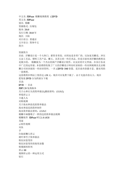
一、可控硅模块PK55FG160的概述可控硅模块PK55FG160是一种半导体器件,常用于交流电路的控制和调节。
它采用了先进的硅控技术,具有高性能和可靠性,广泛应用于工业电力控制系统中。
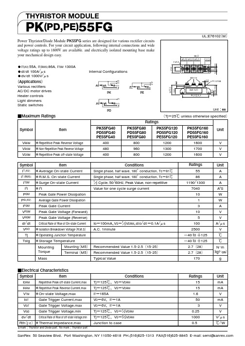
二、可控硅模块PK55FG160的外部参数1. 封装形式:TO-240AC2. 额定电压:1600V3. 额定电流:55A4. 最大耐压:2500V5. 控制电压范围:±20V6. 门极触发电流:200mA7. 工作温度范围:-40℃~125℃8. 重量:约200g三、可控硅模块PK55FG160的主要特性1. 高可靠性:采用优质硅材料和先进封装工艺,具有良好的抗电压和温度特性,能够在恶劣环境下稳定运行。
2. 高性能:具有快速响应和精准控制能力,能够快速稳定地调节电路的工作状态。
3. 低功耗:采用低功率设计,能够有效降低能耗和发热,并延长设备的使用寿命。
4. 灵活性强:可以根据实际需求进行多种控制方式的设计,满足不同应用场景的需求。
5. 绝缘性能优秀:具有良好的绝缘性能,能够有效隔离高压电路和低压控制电路,保证电路的安全稳定运行。
四、可控硅模块PK55FG160的应用领域1. 工业电力控制系统:可控硅模块PK55FG160常用于工业电动机的调速控制、照明设备的亮度调节、电炉的加热控制等领域。
2. 汽车电子系统:可控硅模块PK55FG160被广泛应用于车载充电桩、电动车电池管理系统、电动风扇等领域。
3. 动力电子设备:可控硅模块PK55FG160可以作为逆变器、变频器、整流器等动力电子设备的核心元件,并广泛应用于太阳能、风能发电系统中。
4. 家用电器:可控硅模块PK55FG160常用于电磁炉、电热水器、电烤箱等家用电器的电路控制中。
五、可控硅模块PK55FG160的产品优势1. 高稳定性:采用先进的硅控技术和优质材料,具有出色的稳定性和可靠性。
2. 高性价比:性能优越,价格合理,具有很高的性价比。
3. 安全可靠:通过严格的质量控制和检测,确保产品的安全可靠性。
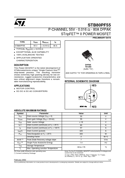
1/7PRELIMINARY DATAFebruary 2002This is preliminary information on a new product now in development or undergoing evaluation. Details are subject to change without notice.STB80PF55P-CHANNEL 55V - 0.016 Ω - 80A D 2PAKSTripFET™ II POWER MOSFETs TYPICAL R DS (on) = 0.016 Ωs EXCEPTIONAL dv/dt CAPABILITY s 100% AVALANCHE TESTED sAPPLICATION ORIENTED CHARACTERIZATIONDESCRIPTIONThis Power MOSFET is the latest development of STMicroelectronis unique "Single Feature Size™"strip-based process. The resulting transistor shows extremely high packing density for low on-resistance, rugged avalanche characteristics and less critical alignment steps therefore a remark-able manufacturing reproducibility.APPLICATIONSs MOTOR CONTROLs DC-DC & DC-AC CONVERTERSTYPE V DSS R DS(on)I D STB80PF5555 V< 0.018 Ω80 AABSOLUTE MAXIMUM RATINGSPulse width limited by safe operating area(*) Current Limited by PackageNote: For the P-CHANNEL MOSFET actual polarity of voltages and current has to be reversed(1)I SD ≤ 40A, di/dt ≤ 300A/µs, V DD ≤ V(BR)DSS , T j ≤ T JMAX.(2) Starting T j = 25 o C, I D = 80A, V DD = 40VSymbol ParameterValue Unit V DS Drain-source Voltage (V GS = 0)55V V DGR Drain-gate Voltage (R GS = 20 k Ω)55V V GS Gate- source Voltage± 16V I D (*)Drain Current (continuos) at T C = 25°C 80A I D Drain Current (continuos) at T C = 100°C 57A I DM (•)Drain Current (pulsed)320A P tot Total Dissipation at T C = 25°C 300W Derating Factor2W/°C dv/dt (1)Peak Diode Recovery voltage slope 7V/ns E AS (2)Single Pulse Avalanche Energy 1.4mJ T stg Storage Temperature-55 to 175°CT jMax. Operating Junction TemperatureSTB80PF552/7THERMAL DATAELECTRICAL CHARACTERISTICS (T case = 25 °C unless otherwise specified)OFFON (*)DYNAMICRthj-case Rthj-ambT lThermal Resistance Junction-case Thermal Resistance Junction-ambientMaximum Lead Temperature For Soldering PurposeMax Max Typ0.562.5300°C/W °C/W °CSymbol ParameterTest ConditionsMin.Typ.Max.Unit V (BR)DSS Drain-sourceBreakdown Voltage I D = 250 µA, V GS = 055V I DSSZero Gate VoltageDrain Current (V GS = 0)V DS = Max RatingV DS = Max Rating T C = 125°C 110µA µA I GSSGate-body Leakage Current (V DS = 0)V GS = ± 16 V±100nASymbol ParameterTest ConditionsMin.Typ.Max.Unit V GS(th)Gate Threshold Voltage V DS = V GS I D = 250 µA 234V R DS(on)Static Drain-source On ResistanceV GS = 10 VI D = 40 A0.0160.018ΩSymbol ParameterTest ConditionsMin.Typ.Max.Unit g fs Forward Transconductance V DS > I D(on) x R DS(on)max, I D =40 A32S C iss C oss C rssInput Capacitance Output Capacitance Reverse Transfer CapacitanceV DS = 25V, f = 1 MHz, V GS = 055001130600pF pF pF3/7STB80PF55SWITCHING ON (*)SWITCHING OFF (*)SOURCE DRAIN DIODE (*)(*) Pulse width [ 300 µs, duty cycle 1.5 %.(•) Pulse width limited by T JMAXSymbol ParameterTest ConditionsMin.Typ.Max.Unit t d(on)t r Turn-on Delay Time Rise TimeV DD = 25 VI D = 40 A R G =4.7 Ω V GS = 10 V (Resistive Load, Figure 3)35190ns ns Q g Q gs Q gdTotal Gate Charge Gate-Source Charge Gate-Drain ChargeV DD = 25 V I D = 80 A V GS = 10V1902765258nC nC nCSymbol ParameterTest ConditionsMin.Typ.Max.Unit t d(off)t f Turn-off Delay Time Fall TimeV DD = 25 VI D = 40 A R G =4.7 Ω V GS = 10 V (Resistive Load, Figure 3)16580ns ns t r(Voff)t f t cOff-voltage Rise Time Fall TimeCross-over TimeV clamp = 40 VI D = 80 A R G =4.7 Ω V GS = 10 V (Inductive Load, Figure 5)604085ns ns nsSymbol ParameterTest ConditionsMin.Typ.Max.Unit I SD I SDM (•)Source-drain CurrentSource-drain Current (pulsed)80320A A V SD (*)Forward On Voltage I SD = 80 AV GS = 01.3V t rr Q rr I RRMReverse Recovery Time Reverse Recovery Charge Reverse Recovery CurrentI SD = 80 Adi/dt = 100A/µs V DD = 25 V T j = 150°C (see test circuit, Figure 5)1104959ns nC AELECTRICAL CHARACTERISTICS (continued)STB80PF554/7Fig. 3: Switching Times Test Circuits For ResistiveFig. 5: Test Circuit For Inductive Load SwitchingSTB80PF55DIM.mm.inch.MIN.TYP. MAX.MIN.TYP. TYP.A 4.4 4.60.1730.181 A1 2.49 2.690.0980.106 A20.030.230.0010.009 B0.70.930.0280.037 B2 1.14 1.70.0450.067 C0.450.60.0180.024 C2 1.21 1.360.0480.054 D8.959.350.3520.368 D180.315E1010.40.3940.409 E18.50.334G 4.88 5.280.1920.208 L1515.850.5910.624 L2 1.27 1.40.0500.055 L3 1.4 1.750.0550.069 M 2.4 3.20.0940.126 R0.40.016V20°8°0°8°D2PAK MECHANICAL DATASTB80PF556/7DIM.mm inchMIN.MAX.MIN.MAX.A010.510.70.4130.421B015.715.90.6180.626D 1.5 1.60.0590.063D1 1.59 1.610.0620.063E 1.65 1.850.0650.073F11.411.60.4490.456K0 4.8 5.00.1890.197P0 3.9 4.10.1530.161P111.912.10.4680.476P2 1.9 2.100750.082R50 1.574T0.250.35.0.00980.0137W23.724.30.9330.956DIM.mm inchMIN.MAX.MIN.MAX.A33012.992B 1.50.059C12.813.20.5040.520D20.20.795G24.426.40.960 1.039N100 3.937T30.4 1.197BASE QTY BULK QTY10001000REEL MECHANICAL DATA* on sales typeTUBE SHIPMENT (no suffix)* TAPE AND REEL SHIPMENT (suffix ”T4”)*D2PAK FOOTPRINTTAPE MECHANICAL DATASTB80PF55 Information furnished is believed to be accurate and reliable. However, STMicroelectronics assumes no responsibility for the consequences of use of such information nor for any infringement of patents or other rights of third parties which may result from its use. No license is grantedby implication or otherwise under any patent or patent rights of STMicroelectronics. Specifications mentioned in this publication are subject to change without notice. This publication supersedes and replaces all information previously supplied. STMicroelectronics products are notauthorized for use as critical components in life support devices or systems without express written approval of STMicroelectronics.The ST logo is registered trademark of STMicroelectronics® 2002 STMicroelectronics - All Rights ReservedAll other names are the property of their respective owners.STMicroelectronics GROUP OF COMPANIESAustralia - Brazil - Canada - China - Finland - France - Germany - Hong Kong - India - Israel - Italy - Japan - Malaysia - Malta - Morocco - Singapore - Spain - Sweden - Switzerland - United Kingdom - United States.7/7。

VishayLow Profile 3mm DC/DC Buck Converter0.8V to 4.5V*, 3A with 380W/in3 Power DensityEfficiency up to 95%FEATURES•Fully integrated DC/DC converter•Advanced development of FX5545G305•High efficiency over large load range•100% duty cycle•Power density - more than 380W/inch3•1µA shutdown current•2.5V to 6V input range (1Li+ and 3-cell NiCd or NiMH cells)•0.8V to 4.5V* output voltage•Programmable PWM/PSM controls•Low output ripple•BGA construction•Temperature range: - 40°C to + 85°C•No external components required•Output power 10W•Maximum current 3A•Low profile*Note: For higher putput voltage please consult factory atFunctionPAK@The DC/DC converter is a programmable topology synchronized Buck converter for today’s continuous changing portable electronic market. The DC/DC converter provides flexibility of utilizing various battery configurations and chemistries such as NiCd, NiMH, or Li+ with an input voltage range of 2.5V to 6V. An additional flexibility is provided with topology programmability to power multiple loads such as power amplifiers, microcontrollers, or baseband logic IC’s. For ultra-high efficiency, converters are designed to operate in synchronous rectified PWM mode under full load while transforming into externally controlled The DC/DC converter is available in 20-ports BGA package. In order to satisfy the stringent ambient temperature requirements, the DC/DC converter is designed to handle the industrial temperature range of - 40°C to + 85°C.APPLICATION•Cordless phones, PDAs and others•Supply voltage source for low-voltage chip sets•Point of Load (POL) applications such as drivers for FPGA’s, microprocessors, DSP’s amplifiers, etc.•Portable computers•Battery back-up supplies•CamerasORDERING INFORMATIONFX5545G008FUNCTIONSIZECIRCUIT IDENTIFIER - G008 or G018OUTPUT VOLTAGE - Example: 1.2V should be written as 1V2 as the V indicates the decimal point or ADJ for adjustable version - self selectable output voltage. G018ADJ is only available in the adjustable version for Vout = 0.9V - 1.3V. For design considerations please see ANF110PACKAGING - B1 = 10pcs in bulk; B5 = 50pcs in bulk; T1 = 13” reel; T2 = 7” reel.For lead (Pb)-free solder please add E2 suffix.VishayDIMENSIONS in inches [millimeters]L0.58 ± 0.01[14.7 ± 0.25]W0.48 ± 0.01[12.2 ± 0.25]A0.1 ± 0.01[2.54 ± 0.25]B0.09 ± 0.01[2.29 ± 0.25]C0.09 ± 0.01[2.27 ± 0.25]T0.126 max[3.2 max]Ball Diameter0.03 ± 0.001[0.762 ± 0.025]/doc?10119For adjustable version please refer to Self Selectable Output Voltageapplication note which is available at /doc?10116**Note: if not used must be connected ti Vin.***Note: N/C - If the output voltage is 0.9V and higher. For outputvoltage of 0.8V connect Vref to MCL4448 (Vishay RF PIN Diode).BOTTOM SIDEPIN CONFIGURATION*PIN CONNECTION1, 2SD3, 7SYNC**4, 8Vref***5, 9Vin6, 10PWM/PSM11, 12N/C13, 17GND14, 18Vout15, 19N/C16, 20GNDPin Configuration for Vo = 0.8V Pin Configuration for Vo = 0.9V - 4.5VRECOMMENDED PAD PATTERN in inches [millimeters]A D F0.1 ± 0.01[2.54 ± 0.25]0.03 ± 0.001[0.8 ± 0.02]0.02 ± 0.001[0.5 ± 0.02]TAPE AND REELSee Tape and Reel Information - T ype BVishay*Note: W D = Power DissipatedSTANDARD ELECTRICAL SPECIFICATIONSPARAMETER UNITCONDITIONMINTYPMAX InputVoltage Range V DC2.56Quiescent Current µAPSM mode 200Soft Start Time ms T SS for Vout = 3.3V 4T SS for Vout = 1.2V 2.6SD, PWM/PSM,SYNC Logic High V V H 2.4Logic Low VV L 0.8Normal Mode µA I DD 750PSM ModeµA I DD 250Shutdown Mode µAI DD1Shutdown Time ms T SS for Vout = 3.3V 4T SS for Vout = 1.2V 0.6Insulation T est Voltage V AC 60Hz 60sec 750ResistanceΩV ISO = 500 V DC 1 x 10¹¹Leakage Current nA V ISO = 500 V DC5Output Power W 10VoltageV DC 0.8 to 4.5Voltage T olerance%For Vout = 0.9V and above (using external diode BAR065V forVout = 0.9V up to 1.3V) at 25°C Ambient T emp.- 3+3%For Vout = 0.8V up to 1.3V using external diode MCL4448 at25°C Ambient T emp.- 5+5T emp. Coefficient %/°C 0.15Ripple and Noise mVpp DC to 20 MHz80GeneralPackage Weight gr. 1.4Oscillator Frequency KHz 400SYNC Range F SYNC /F OSC1.2 1.5Temperature Operation °C - 40+ 85Storage °C - 55+ 125Operating Junction T emp.°C T j 150Thermal Impedance °C/W D *θJA82Rise Time Rise Time (PWM mode): Vin = 6V; Vout = 3.3V; lout = 3A Fall TimeFall Time (PWM mode): Vin = 6V; Vout = 3.3V; lout = 3AVishayPWM MODEVout Vs. lout*Vin = 4.0VVout Vs. Vin*Δ Temp Vs. lout*Above 25°C Ambient Temperature Vin = 6.0V; Vout = 3.3VEfficiency Vs. Lout*Vout = 3.3AVout Vs. lout*Vin = 4.0VVout Vs. Vin*Vin = 6VΔ Temp Vs. lout*Above 25°C Ambient Temperature Vin = 6.0V; Vout = 1.2VEfficiency Vs. lout*Vin = 4.0V; Vout = 1.2V* Note: Measurements were taken with Power supply: ZUP 20-40 from Nemic Lambda; Electronic load: 6063B from Agilent; Multimeter Fluke 45VishayVout Vs. lout* Vin = 4.0V Vout Vs. Vin*Vin = 6VEfficiency Vs. lout*Vin = 4.0V; Vout = 3.3VVout Vs. lout*Vin = 4.0VVout Vs. Vin*Efficiency Vs. lout*Vin = 4.0V; Vout = 1.2VPSM MODE* Note: Measurements were taken with Power supply: ZUP 20-40 from Nemic Lambda; Electronic load: 6063B from Agilent; Multimeter Fluke 45。

BS62LV1600FI55中⽂资料Very Low Power CMOS SRAM 2M X 8 bitBS62LV1600Pb-Free and Green package materials are compliant to RoHSn FEATURESWide V CC operation voltage : 2.4V ~ 5.5V Very low power consumption : V CC = 3.0V Operation current : 46mA (Max.) a t 55ns 2mA (Max.) at 1MHz Standby current : 1.5uA (Typ.) at 25 O C V CC = 5.0V Operation current : 115mA (Max.) a t 55ns 10mA (Max.) a t 1MHz Standby current : 6.0uA (Typ.) at 25O C ? High speed access time : -55 55ns (Max.) at V CC :3.0~5.5V -70 70ns (Max.) at V CC : 2.7~5.5V ? Automatic power down when chip is deselected ? Easy expansion with CE1, CE2 and OE options ? Three state outputs and TTL compatible ? Fully static operation ? Data retention supply voltage as low as 1.5V n DESCRIPTIONThe BS62LV1600 is a high performance, very low power CMOS Static Random Access Memory organized as 2048K by 8 bits and operates form a wide range of 2.4V to 5.5V supply voltage.Advanced CMOS technology and circuit techniques provide both high speed and low power features with typical CMOS standby current of 1.5uA at 3.0V/25O C and maximum access time of 55ns at 3.0V/85O C.Easy memory expansion is provided by an active LOW chip enable (CE1), an active HIGH chip enable (CE2), and active LOW output enable (OE) and three-state output drivers.The BS62LV1600 has an automatic power down feature, reducing the power consumption significantly when chip is deselected. The BS62LV1600 is available in JEDEC standard 44-pin TSOP II and 48-ball BGA package.n POWER CONSUMPTIONPOWER DISSIPATIONSTANDBY(I CCSB1, Max)Operating(I CC , Max)V CC =5.0V V CC =3.0V PRODUCT FAMILYOPERATING TEMPERATUREV CC =5.0V V CC =3.0V1MHz10MHzf Max. 1MHz10MHzf Max.PKG TYPEBS62LV1600EC TSOP II-44 BS62LV1600FC Commercial +0O C to +70O C 50uA 8.0uA 9mA 48mA 113mA 1.5mA 19mA 45mABGA-48-0912 BS62LV1600EITSOP II-44 BS62LV1600FIIndustrial -40O C to +85O C100uA 16uA 10mA 50mA 115mA 2mA 20mA 46mABGA-48-0912n PIN CONFIGURATIONSn BLOCK DIAGRAMBrilliance Semiconductor, Inc. reserves the right to change products and specifications without notice.G H F E D C B A 1 2 3 4 5 6 A9 A11 A10 A19A12 A14 A13 A15 WE NC NC NC DQ7 A17 A16 A7 VSS VCC DQ2 DQ1 DQ6 DQ5 NC A5 OE A3 A0 A6 A4 A1A2CE2 NC NC NCCE1 DQ4 NC 48-ball BGA top view NC NC DQ0 VSS VCC DQ3 NC A18 A20 A8n TRUTH TABLEn ABSOLUTE MAXIMUM RATINGS (1)SYMBOL PARAMETER RATING UNITSV TERM Terminal Voltage withRespect to GND-0.5(2) to 7.0 VT BIAS Temperature UnderBias-40 to +125 O CT STG Storage Temperature -60 to +150 O CP T Power Dissipation 1.0 WI OUT DC Output Current 20 mA1. Stresses greater than those listed under ABSOLUTE MAXIMUM RATINGS may cause permanent damage to the device. This is a stress rating only and functional operation of the device at these or any other conditions above those indicated in the operational sections of this specification is not implied. Exposure to absolute maximum rating conditions for extended periods may affect reliability.2. –2.0V in case of AC pulse width less than 30 ns. n OPERATING RANGERANGAMBIENTTEMPERATUREV CC Commercial 0O C to + 70O C 2.4V ~ 5.5VIndustrial -40O C to + 85O C 2.4V ~ 5.5Vn CAPACITANCE (1) (T A = 25O C, f = 1.0MHz) SYMBOL PAMAMETER CONDITIONS MAX. UNITS C INInputCapacitanceV IN = 0V 10 pFC IOInput/OutputCapacitanceV I/O = 0V 12 pF1. This parameter is guaranteed and not 100% tested.n DC ELECTRICAL CHARACTERISTICS (T A =-40O C to +85OC)1. Typical characteristics are at T A =25O C and not 100% tested.2. Undershoot: -1.0V in case of pulse width less than 20 ns.3. Overshoot: V CC +1.0V in case of pulse width less than 20 ns.4. F MAX =1/t RC.5. I CC(MAX.) is 45mA/113mA at V CC =3.0V/5.0V and T A =70O C.6. I CCSB1(MAX.) is 8.0uA/50uA at V CC =3.0V/5.0V and T A =70O C.n DATA RETENTION CHARACTERISTICS (T A = -40O C to +85OC)1. V CC =1.5V, T A =25O C and not 100% tested.2. t RC = Read Cycle Time.3. I CCRD(Max.) is4.0uA at T A =70O C.n LOW V CC DATA RETENTION WAVEFORM (1) (CE1 Controlled)Data Retention Mode V CCt CDRV CC t RV IHV IHCE1≧V CC - 0.2V V DR ≧1.5V CE1V CCn LOW V CC DATA RETENTION WAVEFORM (2) (CE2 Controlled)n AC TEST CONDITIONS (Test Load and Input/Output Reference)Input Pulse Levels Vcc / 0V Input Rise and Fall Times 1V/ns Input and Output Timing Reference Level 0.5Vcc t CLZ , t OLZ , t CHZ , t OHZ , t WHZ C L = 5pF+1TTL Output LoadOthersC L = 30pF+1TTL1. Including jig and scope capacitance.n KEY TO SWITCHING WAVEFORMSn AC ELECTRICAL CHARACTERISTICS (T A = -40O C to +85OC)READ CYCLECE2 Data Retention Mode V CC t CDR V CC t R V ILV IL V CCV DR ≧1.5V CE2≦0.2V 1 TTL ALL INPUT PULSES→← 90%V CC GND Rise Time : 1V/ns Fall Time : 1V/ns90%→← 10%10%n SWITCHING WAVEFORMS (READ CYCLE)READ CYCLE 1 (1,2,4)READ CYCLE 2 (1,3,4)READ CYCLE 3 (1, 4)NOTES:1. WE is high in read Cycle.2. Device is continuously selected when CE1 = V IL and CE2= V IH .3. Address valid prior to or coincident with CE1 transition low and/or CE2 transition high.4. OE = V IL .5. Transition is measured ± 500mV from steady state with C L = 5pF. The parameter is guaranteed but not 100% tested. t RC t OHt AA D OUT ADDRESS t OHD OUTCE2 CE1D OUTCE2 CE1 OE ADDRESSn AC ELECTRICAL CHARACTERISTICS (T A = -40OC to +85OC)WRITE CYCLEn SWITCHING WAVEFORMS (WRITE CYCLE)WRITE CYCLE 1 (1)t WCt WR1(3)t CW(11)t CW(11)t WP(2)t AWt OHZ(4,10)t AS t WR2(3)t DHt DWD IND OUTWECE2CE1OEADDRESS(5)(5)WRITE CYCLE 2 (1,6)NOTES:1. WE must be high during address transitions.2. The internal write time of the memory is defined by the overlap of CE1 and CE2 active and WE low. All signals must be active to initiate a write and any one signal can terminate a write by going inactive. The data input setup and hold timing should be referenced to the second transition edge of the signal that terminates the write.3. t WR is measured from the earlier of CE1 or WE going high or CE2 going low at the end of write cycle.4. During this period, DQ pins are in the output state so that the input signals of opposite phase to the outputs must not be applied.5. If the CE1 low transition or the CE2 high transition occurs simultaneously with the WE low transitions or after the WE transition, output remain in a high impedance state.6. OE is continuously low (OE = V IL ).7. D OUT is the same phase of write data of this write cycle. 8. D OUT is the read data of next address.9. If CE1 is low and CE2 is high during this period, DQ pins are in the output state. Then the data input signals of opposite phase to the outputs must not be applied to them. 10. T ransition is measured ± 500mV from steady state with C L = 5pF. The parameter is guaranteed but not 100% tested. 11. t CW is measured from the later of CE1 going low or CE2 going high to the end of write.D IND OUTWE CE2 CE1ADDRESSn ORDERING INFORMATIONBSI (Brilliance Semiconductor Inc.) assumes no responsibility for the application or use of any product or circuit described herein. BSI does not authorize its products for use as critical components in any application in which the failure of the BSI product may be expected to result in significant injury or death, including life-support systems and critical medical instruments.n PACKAGE DIMENSIONSTSOP II-44n PACKAGE DIMENSIONS (continued)3: SYMBOL "N" IS THE NUMBER OF SOLDER BALLS.1: CONTROLLING DIMENSIONS ARE IN MILLIMETERS. 2: PIN#1 DOT MARKING BY LASER OR PAD PRINT.N EDNOTES:4812.09.0E1D1e3.755.250.75 48 mini-BGA (9mm x 12mm)n Revision HistoryRevision No. History Draft Date Remark2.2 Add Icc1 characteristic parameter Jan. 13, 2006Improve Iccsb1 spec.I-grade from 220uA to 100uA at 5.0V20uA to 16uA at 3.0VC-grade from 110uA to 50uA at 5.0V10uA to 8.0uA at 3.0V2.3 Change I-grade operation temperature range May. 25, 2006 - from –25O C to –40O C。
7SHIELD 屏蔽SHIELD屏蔽3. Setting Mode Chart设置模式示意图3-1. Screen Composition 界面组成3-2. Message Screen 信息界面3-3. The Way of Setting 设置方法3-3-1. Selecting Analog Filter 选择模拟滤波器Vibration in the process control not only causes fluctuating weight display, but also inaccurate batch weights. The motors, mixers, blenders, screw feeders and vibrators are necessary parts to any automation weighing systems but each can introduce a unique vibratory force to the scale. To adjust analog filter to suit to the weighing systems improves batch quality, speed up the processing and eliminates wasted materials.过程控制中的振动不仅会引起重量显示波动,而且会使得定量重量不准确。
电机,搅拌器,螺旋给料器和振动机是任何一个自动称重系统所必须的部分,但是其中任何一个都可以给秤施加一个单独的振动力。
调整模拟滤波器,使其适合称重系统,提高定量质量,加快称重过程,消除物料浪费。
1)Press button. 按按钮2)Select the "OPERATION" tag.选择“OPERATION”键3)Select the "Analog Filter", choose the analog filter within 2 Hz, 4 Hz, 6 Hz or 8 Hz. The lower frequency is for killing strong vibration, to make the best choice to your system please.选择"Analog Filter",滤波器的频率有2 Hz, 4 Hz, 6Hz或者8Hz。
中文名: JDPaint 精雕视频教程12DVD英文名: JDPaint别名: 精雕资源格式: 压缩包版本: 2010发行日期: 2010年地区: 大陆对白语言: 普通话文字语言: 简体中文简介:资源简介目前,浮雕设计是一个大热门,薪资非常高,应用也是非常广的,比如家具雕花,冲压五金工艺品,塑料工艺产品,雕玉,及其它的一些艺术品。
但是目前培训浮雕的教程还是极少的,精雕做为一个杰出的国产浮雕设计软件,以友好的中文界面,在各行各业中广泛的运用着。
本套教程收集了广大的浮雕设计师实时录制的一些实例视频及北京精雕公司培训部的一些培训资料,一共12DVD 50G容量,是目前内容最丰富,最实用的一套教程。
这套教程在网站上售价达150元,现在可以免费下载了。
由于光盘内容太大,现在把每张DVD分为四部分下载目录:DVD一目录JDP5.20免狗版本关于山和石头的简单做法(播放密码:151315)单线祥云2卡通人头对称视频关于海水和浪花的简单做法海水和浪花的简单制作海水简单做法密码:151315精雕中画像绳子一样的边的简单做法视频精雕软件JDPaint V5.21.0.1028龙退云制作视频双鱼手扫掠面懒人祥云树叶和竹子简单做法特征封套变形特征封套变形的使用录像特徵圆形阵列祥云00视频祥云的一种运用方式钻石制作的头像演示洋花边角视频烟斗老人制作猪头转图小象-描线小象-构建模型拳头烟斗A5加工祥云做法2祥云制作虚拟直纹旋转拉伸面基本操作视频诺诚NC转换器4.0DVD二目录佛头像制作佛头制作佛莲花制作佛身子制作1佛身子制作2佛身子制作3卡通人头描线四叶花制作大象沙发头制作大象沙发头描线手雷0手雷2描线1老爷爷描线花荷花荷花描线车轮制作骏马制作鳞片制作视频方法1视频(有声)鳞片制作视频方法2视频(有声)DVD三目录ENG转NC教程JD5.20转JD5.19五角星清角刀具路径模拟刀路刀路详解79分钟(有声)处理精雕区域雕刻底不平的方法(有声)残料清根视频精雕螺纹下刀模拟录象精雕输出NC刀路有声视频路径问题视频(有声)皮带扣教程花扣骷髅纽扣制作荷花鱼视频2菊花叶子视频一朵梅花简单视频花的浮雕教程(有声)荷花1西洋花制作2DVD四目录欧式花纹描线01十指紧扣卡通兔全过程描线牛描线牛黄猴描线猴浮雕制作玉雕兔制作玉雕马的制作真牛描线花草描线马描线马浮雕制作鱼描线鸡描线龙描线浮雕视频教程1-1.ziped2k://|file|%E6%B5%AE%E9%9B%95%E8%A7%86%E9%A2%91%E6%95%99%E7%A8 %8B1-1[].zip|958384874|8964b4c0eb7ad7be12300a1f96051a0a|h=ojiqf44ssddocpuukcvcwryertgqlqpy|/浮雕视频教程1-2.ziped2k://|file|%E6%B5%AE%E9%9B%95%E8%A7%86%E9%A2%91%E6%95%99%E7%A8 %8B1-2[].zip|890414190|1028f2e09adfffc02858c5ecd68d9087|h=ms3iefrbfxshem2cl4u267p32xbgkfjf|/浮雕视频教程1-3.ziped2k://|file|%E6%B5%AE%E9%9B%95%E8%A7%86%E9%A2%91%E6%95%99%E7%A8 %8B1-3[].zip|969704702|ce7ccd78c28b5c8a7d7ede15ba84379b|h=7rtle7fufoixqctqoaarnkfrf75nyqth|/浮雕视频教程1-4.ziped2k://|file|%E6%B5%AE%E9%9B%95%E8%A7%86%E9%A2%91%E6%95%99%E7%A8 %8B1-4[].zip|439960589|a377610144eb64f556fe2f9e8d3695d1|h=rtehjhgxtmmectnkmmk2oxyqpyr7htlo|/浮雕视频教程2-1.ziped2k://|file|%E6%B5%AE%E9%9B%95%E8%A7%86%E9%A2%91%E6%95%99%E7%A8 %8B2-1[].zip|396527704|13b68fbce947e38af4c5e47b952deed9|h=3zwyfpdxatuemtibisyxxdbykuc27c32|/浮雕视频教程2-2.ziped2k://|file|%E6%B5%AE%E9%9B%95%E8%A7%86%E9%A2%91%E6%95%99%E7%A8 %8B2-2[].zip|952669806|44899140078c3997f4417b036c79385a|h=qtyrz7ahagjqtpkmvebrq3p7wnhh5kfg|/浮雕视频教程2-3.ziped2k://|file|%E6%B5%AE%E9%9B%95%E8%A7%86%E9%A2%91%E6%95%99%E7%A8 %8B2-3[].zip|937070838|be6cfc40f073fd43c1ec3eb449b61cb1|h=vbl42t2jyyufwmiszoccnfx7p7uotdlt|/浮雕视频教程2-4.ziped2k://|file|%E6%B5%AE%E9%9B%95%E8%A7%86%E9%A2%91%E6%95%99%E7%A8 %8B2-4[].zip|962274352|4702b784e31897aebd9c9e3d1f3c01e1|h=wg54j7zgjxqtulezs3fur3kq72bclpyk|/刀路视频教程3-1.ziped2k://|file|%E5%88%80%E8%B7%AF%E8%A7%86%E9%A2%91%E6%95%99%E7%A8 %8B3-1[].zip|271911054|c526912445573d0512*******d349b45|h=yp3llqw7dcdrsqe6nylwlrktnt5hgrgp|/花浮雕制作3-2.ziped2k://|file|%E8%8A%B1%E6%B5%AE%E9%9B%95%E5%88%B6%E4%BD%9C3-2[].zip|1106820326|9b4a771de412297a2a5758d638bd3f37|h=rsmu2r25n243lowmbu5dwplqjku556tc|/花浮雕制作3-3.ziped2k://|file|%E8%8A%B1%E6%B5%AE%E9%9B%95%E5%88%B6%E4%BD%9C3-3[].zip|306495164|86a9b6c2608c7006aa2726f0d10b2b59|h=4nz3jiep2okrc7rpqycs53npmmfhnbe4|/纽扣制作3-4.ziped2k://|file|%E7%BA%BD%E6%89%A3%E5%88%B6%E4%BD%9C3-4[].zip|706674976|7f07eef0f6b68e179959aedf396ec188|h=2mzib2dvx4mncnouduashslbgiwjinli|/浮雕视频教程4-1.ziped2k://|file|%E6%B5%AE%E9%9B%95%E8%A7%86%E9%A2%91%E6%95%99%E7%A8 %8B4-1[].zip|1360162189|5440ed5ab1cef9cd5a944871e0e46412|h=wiox5vovgc2qj36tgfiary6pvdfqpfxz|/浮雕视频教程4-2.ziped2k://|file|%E6%B5%AE%E9%9B%95%E8%A7%86%E9%A2%91%E6%95%99%E7%A8 %8B4-2[].zip|1125058316|c8879355b95a72ae691369b94412dbb1|h=hxgk2h5tenzjlwhppjzhgmmjdgfne4uk|/浮雕视频教程4-3.ziped2k://|file|%E6%B5%AE%E9%9B%95%E8%A7%86%E9%A2%91%E6%95%99%E7%A8 %8B4-3[].zip|1073956600|34ea1f9eff7185e7a9bc5dcf72db8979|h=g2kujsyysrqistpyklivtmb5fp6poggv|/浮雕视频教程4-4.ziped2k://|file|%E6%B5%AE%E9%9B%95%E8%A7%86%E9%A2%91%E6%95%99%E7%A8 %8B4-4[].zip|1074560019|d2c5e17a5c169bea87bb352b13d5538b|h=go7fd5msv6znib2cddcp7kr3sa55wt37|/浮雕视频教程5-1.ziped2k://|file|%E6%B5%AE%E9%9B%95%E8%A7%86%E9%A2%91%E6%95%99%E7%A8 %8B5-1[].zip|373527662|2ff07b68f1b1b51b34f3df83a7dc21da|h=paqntco4cfqderztgfxzvwqkdpidf6vb|/浮雕视频教程5-2.ziped2k://|file|%E6%B5%AE%E9%9B%95%E8%A7%86%E9%A2%91%E6%95%99%E7%A8 %8B5-2[].zip|1101880705|a06152a3fcfef30673ee9879955fbcb8|h=co3nmb2u45s52acp2jk23uefjmukoz2i|/浮雕视频教程5-3.ziped2k://|file|%E6%B5%AE%E9%9B%95%E8%A7%86%E9%A2%91%E6%95%99%E7%A8 %8B5-3[].zip|1125960331|b0498a91a2bb50773a5b2f8eb868fc72|h=5gyiswftnyryn3hgiylktxi5dxqlixy6|/浮雕视频教程5-4.ziped2k://|file|%E6%B5%AE%E9%9B%95%E8%A7%86%E9%A2%91%E6%95%99%E7%A8 %8B5-4[].zip|1167413647|264f1d414fc59840f65fbc6fa0c113b4|h=nzkzpkm76zwlalxf4gzmtvw5r7om3iw2|/浮雕视频教程6-1.ziped2k://|file|%E6%B5%AE%E9%9B%95%E8%A7%86%E9%A2%91%E6%95%99%E7%A8 %8B6-1[].zip|800302904|3dd6531c851c3e82eb3ab2089e5d7e01|h=234yh62k7v5an67owelrc5ytumlwi55n|/浮雕视频教程6-2.ziped2k://|file|%E6%B5%AE%E9%9B%95%E8%A7%86%E9%A2%91%E6%95%99%E7%A8 %8B6-2[].zip|631163293|f3913d06a9a5ff37694cd1a17549a4cc|h=4wuzj3ra4xx6hpckn2v75evbja4sfuf4|/浮雕视频教程6-3.ziped2k://|file|%E6%B5%AE%E9%9B%95%E8%A7%86%E9%A2%91%E6%95%99%E7%A8 %8B6-3[].zip|1229862564|e9fc6f4f095d08459c476a5780f00d74|h=jknqdzqxuk44vmherunnt7idtqsu7k3b|/浮雕视频教程6-4.ziped2k://|file|%E6%B5%AE%E9%9B%95%E8%A7%86%E9%A2%91%E6%95%99%E7%A8 %8B6-4[].zip|386016204|a85c2d6c98907868cf990eebcddeb282|h=ux26f2o6zrjcsbwkmzuiswqowapq4gwp|/浮雕视频教程7-1.ziped2k://|file|%E6%B5%AE%E9%9B%95%E8%A7%86%E9%A2%91%E6%95%99%E7%A8 %8B7-1[].zip|630756885|7f9c55f36f73b68fbb8f56767d032797|h=3ojaxpf3dmx6g3kzc3bspeql22azqh6s|/浮雕视频教程7-2.ziped2k://|file|%E6%B5%AE%E9%9B%95%E8%A7%86%E9%A2%91%E6%95%99%E7%A8 %8B7-2[].zip|456934068|4187648ded36fdbc5a5d8431955d4276|h=6hhpdtzu3enm2h47iwweja3xrnhxka6b|/二维3D视频教程8-1.ziped2k://|file|%E4%BA%8C%E7%BB%B43D%E8%A7%86%E9%A2%91%E6%95%99%E7 %A8%8B8-1[].zip|571227583|9b6f6a8cc904441927984226b08b997f|h=b7r6wkjzxkngl6k3pmwbezvband5ay7i|/二维3D视频教程8-2.ziped2k://|file|%E4%BA%8C%E7%BB%B43D%E8%A7%86%E9%A2%91%E6%95%99%E7 %A8%8B8-2[].zip|928057130|2ac65ec7f2f566369e498bbb7dd66aec|h=fklillydlwuhl3zfupweshslzpa4kd57|/二维3D视频教程8-3.ziped2k://|file|%E4%BA%8C%E7%BB%B43D%E8%A7%86%E9%A2%91%E6%95%99%E7 %A8%8B8[].zip|851942898|c9b324a295e50b5ade4b35fe40c4572f|h=kudrkuonakfknbdhbqqbff33hkw3pn7d|/精雕资料图片9-1.ziped2k://|file|%E7%B2%BE%E9%9B%95%E8%B5%84%E6%96%99%E5%9B%BE%E7%89 %879-1[].zip|324253986|99afa6e6b964da45637ab85a7308a8ba|h=ectythayihpm73643pgbko7mdbgw6lkc|/精雕资料图片9-2.ziped2k://|file|%E7%B2%BE%E9%9B%95%E8%B5%84%E6%96%99%E5%9B%BE%E7%89 %879-2[].zip|497007989|7df6ce79575bae7e3605acb44d97c48d|h=6ifzfpegod33g6f7z7wsmxy23cwhqrmn|/精雕资料图片9-3.ziped2k://|file|%E7%B2%BE%E9%9B%95%E8%B5%84%E6%96%99%E5%9B%BE%E7%89 %879-3[].zip|270113716|641d0fd955140baf6499b5506a3abd0a|h=mbesatcwbxikps2xbyby2g5pofu4nagp|/精雕资料图片9-4.ziped2k://|file|%E7%B2%BE%E9%9B%95%E8%B5%84%E6%96%99%E5%9B%BE%E7%89 %879-4[].zip|272881244|511b3b93897c5471674680d38d7f7ddf|h=6r236f6hah45u5trco6u4gesvuzolvwe|/精雕入门篇10-1.ziped2k://|file|%E7%B2%BE%E9%9B%95%E5%85%A5%E9%97%A8%E7%AF%8710-1[].zip|308501422|ee10750e5e3f0a1903aa4c264b71b7ec|h=i3y6x3djt4q6gi4zntk2ewx3zbfnbqzr|/精雕入门篇10-2.ziped2k://|file|%E7%B2%BE%E9%9B%95%E5%85%A5%E9%97%A8%E7%AF%8710-2 [].zip|235019938|6f29ebe10926ae32124af3669412ebb9|h=qmk6nyy45 wuelyzgtv5wcpaxrhblnbk2|/精雕入门篇10-3.ziped2k://|file|%E7%B2%BE%E9%9B%95%E5%85%A5%E9%97%A8%E7%AF%8710-3 [].zip|263956993|5caabfd131f8b2a07977af6ba8b5a336|h=6eydlysisgks6i4xmdtaavq3lmmc7hwz|/精雕入门篇10-4.ziped2k://|file|%E7%B2%BE%E9%9B%95%E5%85%A5%E9%97%A8%E7%AF%8710-4 [].zip|185882935|99ca822df26ee62490a1fe5eb6c8079f|h=7l4icz6uc7ecgcygb6dzeo42yaqnmsa5|/精雕入门篇11-1.ziped2k://|file|%E7%B2%BE%E9%9B%95%E5%85%A5%E9%97%A8%E7%AF%8711-1 [].zip|688205649|58f08b7aa34dbe9f99dbefc958dc4a20|h=b7irfz7gxa7ye46jsbutdu5ff7ihhtcg|/精雕入门篇11-2.ziped2k://|file|%E7%B2%BE%E9%9B%95%E5%85%A5%E9%97%A8%E7%AF%8711-2 [].zip|170523189|71bcd6aa5e8320306325e4c7df252e37|h=y6hy6i7kh tcapia4crp7bt33ijkm5vcj|/精雕入门篇11-3.ziped2k://|file|%E7%B2%BE%E9%9B%95%E5%85%A5%E9%97%A8%E7%AF%8711-3 [].zip|316092022|c9b9e99dbe1f02c99a6d8a867ac2c965|h=vksiadb3kev4lhb3x2b5cdw4j36xbbdu|/精雕入门篇11-4.ziped2k://|file|%E7%B2%BE%E9%9B%95%E5%85%A5%E9%97%A8%E7%AF%8711-4[].zip|295763492|fd2b34e3315b86075ad70a3657803f80|h=dev2hw6zurwilupepviryd67b3rvof6r|/精雕入门篇12-1.ziped2k://|file|%E7%B2%BE%E9%9B%95%E5%85%A5%E9%97%A8%E7%AF%8712-1[].zip|967654253|e75425a07bc9c98cccf67a9eceed76ee|h=gls52l5eyv4ezf65p3m7hzxj753mkfji|/精雕入门篇12-2.ziped2k://|file|%E7%B2%BE%E9%9B%95%E5%85%A5%E9%97%A8%E7%AF%8712-2[].zip|995041531|6f8251a5ca53681d8faae52c7d98932b|h=mm2fptdihubefdbqcucmtwzsetpsq5b5|/精雕入门篇12-3.ziped2k://|file|%E7%B2%BE%E9%9B%95%E5%85%A5%E9%97%A8%E7%AF%8712-3[].zip|1006592067|b4f2446da91859b7567c5fed64dfe488|h=qwz32x2eaeozcogdqu2d6xws37rwcxqa|/精雕入门篇12-4.ziped2k://|file|%E7%B2%BE%E9%9B%95%E5%85%A5%E9%97%A8%E7%AF%8712-4[].zip|372040235|710c1d556f8b42e3d1099dc39ca766a3|h=a4lrtd3sng24zgupkv2sfxv4li5yewsn|/4-1中的十指紧扣.ziped2k://|file|4-1%E4%B8%AD%E7%9A%84%E5%8D%81%E6%8C%87%E7%B4%A7%E6 %89%A3[].zip|742368961|5d0053b668c44d25e596eafa0edc81ba|h=odxx4wtj4xjbmtzt6j7tczm7vg7nrgj2|/4-2中的-牛黄.ziped2k://|file|4-2%E4%B8%AD%E7%9A%84-%E7%89%9B%E9%BB%84[].zip|700845295|f1e4a7db08af8dff50c87c2c5f4ccada|h=ty3nbtz4o ybquleo7bnrybxm4iwr2tfg|/。


STB80PF55_06中文资料September 2006 Rev. 51/13STB80PF55STP80PF55P-channel 55V - 0.016? - 80A - TO-220 - D 2P AKSTripFET? II Power MOSFETGeneral features■Extremely dv/dt capability ■100% avalanche tested■Application oriented characterizationDescriptionThis Power MOSFET is the laest development of STMicroelectronics unique “Single feature size?”strip-based process. The resultingtransistor shows extremely high packing density for low on-resistance, rugged avalanchecharacteristics and less critical alignment steps therefore a remarkable manufacturing reproducibility.Applications■Switching applicationType V DSS R DS(on)I D STP80PF5555V <0.018?80A STB80PF5555V<0.018?80AOrder codesPart number Marking Package Packaging STP80PF55P80PF55TO-220T ube STB80PF55B80PF55D 2P AKTape & reelContents STB80PF55 - STP80PF55Contents1Electrical ratings . . . . . . . . . . . . . . . . . . . . . . . . . . . . . . . . . . . . . . . . . . . . 32Electrical characteristics . . . . . . . . . . . . . . . . . . . . . . . . . . . . . . . . . . . . . 42.1Electrical characteristics (curves) . . . . . . . . . . . . . . . . . . . . . . . . . . . . . 6 3Test circuit . . . . . . . . . . . . . . . . . . . . . . . . . . . . . . . . . . . . . . . . . . . . . . . . 8 4Package mechanical data . . . . . . . . . . . . . . . . . . . . . . . . . . . . . . . . . . . . .9 5Revision history . . . . . . . . . . . . . . . . . . . . . . . . . . . . . . . . . . . . . . . . . . .122/13STB80PF55 - STP80PF55Electrical ratings3/131 Electrical ratingsTable 1.Absolute maximum ratingsSymbol ParameterValue Unit V DS Drain-source voltage (V GS = 0)55V V GS Gate-source voltage±16V I D (1)1.Current limited by packageDrain current (continuous) at T C = 25°C 80A I D Drain current (continuous) at T C = 100°C 57A I DM (2)2.Pulse width limited by safe operating area Drain current (pulsed)320A P TOTTotal dissipation at T C = 25°C 300W Derating factor2W/°C dv/dt (3)3.I SD < 40A, di/dt < 300 A/μs, V DD =80% V (BR)DSS Peak diode recovery voltage slope 7V/ns E AS (4)4.Starting Tj=25°C, I D =80A, V DD =40VNote:For the P-CHANNEL MOSFET actual polarity of voltages and current has to be reversed Single pulse avalanche energy 1.4J T j T stgOperating junction temperature Storage temperature-55 to 175°CTable 2.Thermal dataSymbol ParameterValue Unit R thj-case Thermal resistance junction-case max 0.5°C/W R thj-a Thermal resistance junction-ambient max 62.5°C/W T lMaximum lead temperature for soldering purpose300°CElectrical characteristics STB80PF55 - STP80PF554/132 Electrical characteristics(T CASE =25°C unless otherwise specified)Table 3.On/off statesSymbol ParameterTest conditionsMin.Typ.Max.UnitV (BR)DSS Drain-sourcebreakdown voltage I D = 250mA, V GS = 055V I DSS Zero gate voltagedrain current (V GS = 0)V DS = Max ratingV DS = Max rating, T C =125°C 110μA μA I GSS Gate-body leakage current (V DS = 0)V GS = ±16V±10μA V GS(th)Gate threshold voltage V DS = V GS , I D = 250μA 234V R DS(on)Static drain-source on resistanceV GS = 10V , I D = 40A0.0160.018Table 4.DynamicSymbol ParameterTest conditionsMin.Typ.Max.Unitg fs Forward transconductance V DS > I D(on) x R DS(on)max, I D = 40A32S C iss C oss C rss Input capacitance Output capacitance Reverse transfer capacitance V DS = 25V , f = 1MHz, V GS = 0 55001130600pF pF pF Q g Q gs Q gdT otal gate charge Gate-source charge Gate-drain chargeI D = 25A, V DD = 80V ,V GS = 10V(see Figure 14)1902765258nC nC nCSTB80PF55 - STP80PF55Electrical characteristics5/13Table 5.Switching timesSymbol ParameterTest conditions Min.Typ.Max.Unit t d(on)t r Turn-on delay time Rise timeV DD =25V , I D =40A, R G =4.7?, V GS =10V (see Figure 13)35190ns ns t d(off)t f Turn-off delay time Fall timeV DD =25V , I D =40A, R G =4.7?, V GS =10V (see Figure 13)16580ns ns t r(Voff)t f t cOff-voltage rise time Fall timeCross-over timeV clamp =40V , I D =80A, R G =4.7?, V GS =10V (see Figure 13)604085ns ns nsTable 6.Source drain diodeSymbol ParameterTest condictionsMinTyp.Max Unit I SD I SDM (1)1.Pulse width limited by TjmaxSource-drain currentSource-drain current (pulsed)1040A A V SD (2)2.Pulsed: pulse duration = 300 μs, duty cycle 1.5 %Forward on voltage I SD = 80A, V GS = 0 1.6V t rr Q rr I RRMReverse recovery time Reverse recovery charge Reverse recovery currentI SD = 80A, di/dt = 100A/μs V DD = 25V , T j =150°C1104959ns μC AElectrical characteristics STB80PF55 - STP80PF556/132.1 Electrical characteristics (curves)Figure 1.Safe operating area for TO-220Figure 2.Thermal impedance for TO-220Figure 3.Output characterisics Figure 4.Transfer characteristicsFigure 5.Transconductance Figure 6.Static drain-source on resistanceSTB80PF55 - STP80PF55Electrical characteristics7/13Figure 7.Gate charge vs gate-source voltage Figure 8.Capacitance variationsFigure 9.Normalized gate threshold voltageFigure 10.Normalized on resistance vsFigure 11.Source-drain diode forwardFigure 12.Normalized B VDSS vs temperatureTest circuit STB80PF55 - STP80PF558/133 Test circuitFigure 13.Switching times test circuit forFigure 14.Gate charge test circuitFigure 15.Test circuit for inductive loadSTB80PF55 - STP80PF55Package mechanical data 4 Package mechanical dataIn order to meet environmental requirements, ST offers these devices in ECOPACK?packages. These packages have a Lead-free second level interconnect . The category ofsecond level interconnect is marked on the package and on the inner box label, incompliance with JEDEC Standard JESD97. The maximum ratings related to solderingconditions are also marked on the inner box label. ECOPACK is an ST trademark.ECOPACK specifications are available at: 9/13Package mechanical data STB80PF55 - STP80PF5510/13STB80PF55 - STP80PF55Package mechanical data11/13Revision history STB80PF55 - STP80PF5512/135 Revision historyTable 7.Revision historyDate RevisionChanges09-Sep-20044Revalidation12-Sep-20065New template, D 2P AK addedSTB80PF55 - STP80PF55Please Read Carefully:Information in this document is provided solely in connection with ST products. STMicroelectronics NV and its subsidiaries (“ST”) reserve the right to make changes, corrections, modifications or improvements, to this document, and the products and services described herein at any time, without notice.All ST products are sold pursuant to ST’s terms and conditions of sale.Purchasers are solely responsible for the choice, selection and use of the ST products and services described herein, and ST assumes no liability whatsoever relating to the choice, selection or use of the ST products and services described herein.No license, express or implied, by estoppel or otherwise, to any intellectual property rights is granted under this document. If any part of this document refers to any third party products or services it shall not be deemed a license grant by ST for the useof such third party products or services, or any intellectual property contained therein or considered as a warranty covering the use in any manner whatsoever of such third party products or services or any intellectual property contained therein.UNL ESS OTHERWISE SET FORTH IN ST’S TERMS AND CONDITIONS OF SAL E ST DISCL AIMS ANY EXPRESS OR IMPL IED WARRANTY WITH RESPECT TO THE USE AND/OR SAL E OF ST PRODUCTS INCL UDING WITHOUT L IMITATION IMPL IED WARRANTIES OF MERCHANTABILITY, FITNESS FOR A PARTICULAR PURPOSE (AND THEIR EQUIVALENTS UNDER THE LAWS OF ANY JURISDICTION), OR INFRINGEMENT OF ANY PATENT, COPYRIGHT OR OTHER INTELLECTUAL PROPERTY RIGHT. UNL ESS EXPRESSL Y APPROVED IN WRITING BY AN AUTHORIZED ST REPRESENTATIVE, ST PRODUCTS ARE NOT RECOMMENDED, AUTHORIZED OR WARRANTED FOR USE IN MILITARY, AIR CRAFT, SPACE, LIFE SAVING, OR LIFE SUSTAINING APPLICATIONS, NOR IN PRODUCTS OR SYSTEMS WHERE FAILURE OR MALFUNCTION MAY RESULT IN PERSONAL INJURY, DEATH, OR SEVERE PROPERTY OR ENVIRONMENTAL DAMAGE. ST PRODUCTS WHICH ARE NOT SPECIFIED AS "AUTOMOTIVE GRADE" MAY ONLY BE USED IN AUTOMOTIVE APPLICATIONS AT USER’S OWN RISK.Resale of ST products with provisions different from the statements and/or technical features set forth in this document shall immediately void any warranty granted by ST for the ST product or service described herein and shall not create or extend in any manner whatsoever, any liability of ST.ST and the ST logo are trademarks or registered trademarks of ST in various countries.Information in this document supersedes and replaces allinformation previously supplied.The ST logo is a registered trademark of STMicroelectronics. All other names are the property of their respective owners.2006 STMicroelectronics - All rights reservedSTMicroelectronics group of companiesAustralia - Belgium - Brazil - Canada - China - Czech Republic - Finland - France - Germany - Hong Kong - India - Israel - Italy - Japan - Malaysia - Malta - Morocco - Singapore - Spain - Sweden - Switzerland - United Kingdom - United States of America 13/13。

PK55FG160的应用原理1. 简介PK55FG160是一款先进的微控制器芯片,具备高性能和低功耗的特点。
本文将介绍PK55FG160的应用原理以及其在各个领域的应用。
2. PK55FG160的工作原理PK55FG160使用CMOS技术制造,集成了高度集成的处理器核心、存储器、外设以及各种接口电路。
下面将详细介绍PK55FG160的工作原理。
2.1 处理器核心PK55FG160采用了高性能的ARM Cortex-M4核心,具有强大的计算能力和丰富的指令集。
该核心能够处理高速输入输出并实时响应各种控制指令。
2.2 存储器PK55FG160集成了多种存储器,包括闪存、SRAM和EEPROM。
闪存用于存储程序代码和数据,SRAM用于临时存储数据,而EEPROM则用于存储关键的配置参数和数据。
2.3 外设PK55FG160的外设包括模拟输入输出、数字输入输出、通信接口和定时器等。
这些外设能够满足各种应用的需求,例如模拟输入输出可用于采集和输出模拟信号,通信接口可支持UART、SPI、I2C等多种通信协议。
2.4 时钟管理PK55FG160内部集成了多个时钟源,包括内部振荡器和外部晶体振荡器。
通过合理配置时钟源,并利用内部的时钟分频器和时钟树,可以提供适合各种应用的时钟信号。
3. PK55FG160在各个领域的应用PK55FG160具有广泛的应用领域,下面将介绍一些典型的应用案例。
3.1 工业自动化在工业自动化领域,PK55FG160可以用于控制机械臂、传送带、流水线等设备。
通过连接各种传感器和执行器,PK55FG160可以实现精准的控制和自动化操作。
3.2 智能家居PK55FG160可以应用于智能家居系统,用于控制灯光、温度、安防等功能。
通过与云平台的连接,智能家居系统可以实现远程控制和智能化管理。
3.3 汽车电子PK55FG160在汽车电子领域有着广泛的应用。
它可以用于发动机控制、底盘控制、车身电子等方面,提供高性能的计算和实时控制。

KEY FEATURESn 5 Volt Read, Program, and Erase–Minimizes system-level power requirements n High Performance–Access times as fast as 50 ns n Low Power Consumption–20 mA typical active read current in byte mode, 28 mA typical in word mode –35 mA typical program/erase current – 5 µA maximum CMOS standby current n Compatible with JEDEC Standards–Package, pinout and command-set compatible with the single-supply Flash device standard–Provides superior inadvertent write protectionn Sector Erase Architecture–Boot sector architecture with top and bottom boot block options available–One 16 Kbyte, two 8 Kbyte, one 32 Kbyte and fifteen 64 Kbyte sectors in byte mode –One 8 Kword, two 4 Kword, one 16 Kword and fifteen 32 Kword sectors in word mode – A command can erase any combination of sectors–Supports full chip erase n Erase Suspend/Resume–Temporarily suspends a sector eraseoperation to allow data to be read from, or programmed into, any sector not being erased n Sector Protection–Any combination of sectors may be locked to prevent program or erase operations within those sectorsn Temporary Sector Unprotect–Allows changes in locked sectors(requires high voltage on RESET# pin)n Internal Erase Algorithm–Automatically erases a sector, anycombination of sectors, or the entire chip n Internal Programming Algorithm–Automatically programs and verifies data at a specified addressn Fast Program and Erase Times–Byte programming time: 7 µs typical –Sector erase time: 1.0 sec typical –Chip erase time: 19 sec typicaln Data# Polling and Toggle Status Bits–Provide software confirmation of completion of program or erase operationsn Ready/Busy# Output (RY/BY#)–Provides hardware confirmation of completion of program and erase operationsn Minimum 100,000 Program/Erase Cycles n Space Efficient Packaging–Available in industry-standard 44-pin PSOP and 48-pin TSOP and reverse TSOP packages PreliminaryRevision 1.1, February 2002GENERAL DESCRIPTIONThe HY29F800A is an 8 Megabit, 5 volt only CMOS Flash memory organized as 1,048,576 (1M) bytes or 524,288 (512K) words. The device is offered in industry-standard 44-pin PSOP and 48-pin TSOP packages.The HY29F800A can be programmed and erased in-system with a single 5-volt V CC supply. Internally generated and regulated voltages are provided for program and erase operations, so that the device does not require a high voltage power supply to perform those functions. The device can also be programmed in standard EPROM programmers.Access times as fast as 55 ns over the full operat-ing voltage range of 5.0 volts ± 10% are offered for timing compatibility with the zero wait state require-ments of high speed microprocessors. A 50 nsLOGIC DIAGRAMHY29F800A8 Megabit (1Mx8/512Kx16), 5 Volt-only, Flash Memory元器件交易网2Rev. 1.1/Feb 02HY29F800Aversion operating over 5.0 volts ± 5% is also avail-able. To eliminate bus contention, the HY29F800A has separate chip enable (CE#), write enable (WE#) and output enable (OE#) controls.The device is compatible with the JEDEC single power-supply Flash command set standard. Com-mands are written to the command register using standard microprocessor write timings, from where they are routed to an internal state-machine that controls the erase and programming circuits. De-vice programming is performed a byte at a time by executing the four-cycle Program Command.This initiates an internal algorithm that automati-cally times the program pulse widths and verifies proper cell margin.The HY29F800A ’s sector erase architecture allows any number of array sectors to be erased and re-programmed without affecting the data contents of other sectors. Device erasure is initiated by ex-ecuting the Erase Command. This initiates an in-ternal algorithm that automatically preprograms the array (if it is not already programmed) before ex-ecuting the erase operation. During erase cycles,the device automatically times the erase pulse widths and verifies proper cell margin.To protect data in the device from accidental or unauthorized attempts to program or erase the device while it is in the system (e.g., by a virus),the device has a Sector Protect function which hardware write protects selected sectors. The sector protect and unprotect features can be en-abled in a PROM programmer. Temporary Sector Unprotect, which requires a high voltage, allows in-system erasure and code changes in previously protected sectors.Erase Suspend enables the user to put erase on hold for any period of time to read data from, or program data to, any sector that is not selected for erasure. True background erase can thus be achieved. The device is fully erased when shipped from the factory.Addresses and data needed for the programming and erase operations are internally latched during write cycles, and the host system can detect completion of a program or erase operation by observing the RY/BY# pin, or by reading the DQ[7](Data# Polling) and DQ[6] (toggle) status bits.Reading data from the device is similar to reading from SRAM or EPROM devices. Hardware data protection measures include a low V CC detector that automatically inhibits write operations during power transitions.The host can place the device into the standby mode. Power consumption is greatly reduced in this mode.BLOCK DIAGRAM元器件交易网HY29F800A PIN CONFIGURATIONSCONVENTIONSUnless otherwise noted, a positive logic (active High) convention is assumed throughout this docu-ment, whereby the presence at a pin of a higher, more positive voltage (nominally 5VDC) causes assertion of the signal. A ‘#’ symbol following the signal name, e.g., RESET#, indicates that the sig-nal is asserted in a Low state (nominally 0 volts).Whenever a signal is separated into numbered bits, e.g., DQ[7], DQ[6], ..., DQ[0], the family of bits may also be shown collectively, e.g., as DQ[7:0].The designation 0xNNNN (N = 0, 1, 2, . . . , 9, A, . . . , E, F) indicates a number expressed in hexadeci-mal notation. The designation 0bXXXX indicates a number expressed in binary notation (X = 0, 1).元器件交易网3 Rev. 1.1/Feb 02HY29F800AMEMORY ARRAY ORGANIZATIONThe 1 Mbyte Flash memory array is organized into nineteen blocks called sectors (S0, S1, . . . , S18).A sector is the smallest unit that can be erased and which can be protected to prevent accidental or unauthorized erasure. See the ‘Bus Operations’and ‘Command Definitions’ sections of this docu-ment for additional information on these functions. In the HY29F800A, four of the sectors, which com-prise the boot block, vary in size from 8 to 32Kbytes (4 to 16 Kwords), while the remaining fif-teen sectors are uniformly sized at 64 Kbytes (32 Kwords). The boot block can be located at the bottom of the address range (HY29F800AB) or at the top of the address range (HY29F800AT). Table 1 defines the sector addresses and corre-sponding address ranges for the top and bottom boot block versions of the HY29F800A.元器件交易网4Rev. 1.1/Feb 02元器件交易网HY29F800A1.X indicates Don’t Care.2.Address in Byte Mode is A[18:-1].3.Address in Word Mode is A[18:0].5 Rev. 1.1/Feb 02HY29F800A1 Notes:1.L = VIL , H = VIH, X = Don’t Care, DOUT= Data Out, DIN= Data In. See DC Characteristics for voltage levels.2.Address is A[18:-1] in Byte Mode and A[18:0] in Word Mode.3.DQ[15] is the A[-1] input in Byte Mode (BYTE# = L).BUS OPERATIONSDevice bus operations are initiated through the internal command register, which consists of sets of latches that store the commands, along with the address and data information, if any, needed to execute the specific command. The command register itself does not occupy any addressable memory location. The contents of the command register serve as inputs to an internal state ma-chine whose outputs control the operation of the device. Table 2 lists the normal bus operations, the inputs and control levels they require, and the resulting outputs. Certain bus operations require a high voltage on one or more device pins. Those are described in Table 3.Read OperationData is read from the HY29F800A by using stan-dard microprocessor read cycles while placing the address of the byte or word to be read on the device’s address inputs, A[18:0] in Word mode (BYTE# = H) or A[18:-1] in Byte mode (BYTE# = L) . As shown in Table 2, the host system must drive the CE# and OE# inputs Low and drive WE# High for a valid read operation to take place. The device outputs the specified array data on DQ[7:0] in Byte mode and on DQ[15:0] in Word mode. Note that DQ[15] serves as address input A[-1] when the device is operating in Byte mode.The HY29F800A is automatically set for reading array data after device power-up and after a hard-ware reset to ensure that no spurious alteration of the memory content occurs during the power tran-sition. No command is necessary in this mode to obtain array data, and the device remains enabled for read accesses until the command register con-tents are altered.This device features an Erase Suspend mode. While in this mode, the host may read the array data from any sector of memory that is not marked for erasure. If the host attempts to read from an address within an erase-suspended sector, or while the device is performing an erase or byte/ word program operation, the device outputs sta-tus data instead of array data. After completing a programming operation in the Erase Suspend mode, the system may once again read array data with the same exceptions noted above. After com-pleting an internal program or internal erase algo-rithm, the HY29F800A automatically returns to the read array data mode.The host must issue a hardware reset or the soft-ware reset command (see Command Definitions) to return a sector to the read array data mode if DQ[5] goes high during a program or erase cycle, or to return the device to the read array data mode while it is in the Electronic ID mode.Write OperationCertain operations, including programming data and erasing sectors of memory, require the host to write a command or command sequence to the HY29F800A. Writes to the device are performed元器件交易网6Rev. 1.1/Feb 02HY29F800A1, 2Notes:1.L = VIL , H = VIH, X = Don’t Care. See DC Characteristics for voltage levels.2.Address bits not specified are Don’t Care.3.See text for additional information.4.SA = sector address. See Table 1.5.DQ[15] is the A[-1] input in Byte Mode (BYTE# = L).by placing the byte or word address on the device’s address inputs while the data to be written is input on DQ[7:0] in Byte mode (BYTE# = L) and on DQ[15:0] in Word mode (BYTE# = H). The host system must drive the CE# and WE# pins Low and drive OE# High for a valid write operation to take place. All addresses are latched on the fall-ing edge of WE# or CE#, whichever happens later. All data is latched on the rising edge of WE# or CE#, whichever happens first.The ‘Device Commands’ section of this document provides details on the specific device commands implemented in the HY29F800A.Output Disable OperationWhen the OE# input is at VIH , output data from thedevice is disabled and the data bus pins are placed in the high impedance state.Standby OperationWhen the system is not reading from or writing to the HY29F800A, it can place the device in the Standby mode. In this mode, current consump-tion is greatly reduced, and the data bus outputs are placed in the high impedance state, indepen-dent of the OE# input. The Standby mode can invoked using two methods.The device enters the CE# CMOS Standby mode if the CE# and RESET# pins are both held at VCC ± 0.5V. Note that this is a more restricted voltage range than VIH. If both CE# and RESET# are heldHigh, but not within VCC± 0.5V, the device will be in the CE# TTL Standby mode, but the standby current will be greater.The device enters the RESET# CMOS Standbymode when the RESET# pin is held at VSS± 0.5V.If RESET# is held Low but not within VSS± 0.5V, the HY29F800A will be in the RESET# TTL Standby mode, but the standby current will be greater. See Hardware Reset Operation section for additional information on the reset operation.The device requires standard access time (tCE) forread access when the device is in either of the standby modes, before it is ready to read data. If the device is deselected during erasure or pro-gramming, it continues to draw active current until the operation is completed.Hardware Reset OperationThe RESET# pin provides a hardware method ofresetting the device to reading array data. When the RESET# pin is driven Low for the minimum specified period, the device immediately termi-nates any operation in progress, tri-states the data bus pins, and ignores all read/write commands for元器件交易网7 Rev. 1.1/Feb 028Rev. 1.1/Feb 02HY29F800Athe duration of the RESET# pulse. The device also resets the internal state machine to reading array data. If an operation was interrupted by the as-sertion of RESET#, it should be reinitiated once the device is ready to accept another command sequence to ensure data integrity.Current is reduced for the duration of the RESET#pulse as described in the Standby Operation sec-tion above.If RESET# is asserted during a program or erase operation, the RY/BY# pin remains Low (busy) until the internal reset operation is complete, which re-quires a time of t READY (during Automatic Algo-rithms). The system can thus monitor RY/BY# to determine when the reset operation completes,and can perform a read or write operation t RB after RY/BY# goes High. If RESET# is asserted when a program or erase operation is not executing (RY/BY# pin is High), the reset operation is completed within a time of t RP . In this case, the host can per-form a read or write operation t RH after the RE-SET# pin returns High .The RESET# pin may be tied to the system reset signal. Thus, a system reset would also reset thedevice, enabling the system to read the boot-up firmware from the Flash memory.Sector Protect/Unprotect OperationsHardware sector protection can be invoked to dis-able program and erase operations in any single sector or combination of sectors. This function is typically used to protect data in the device from unauthorized or accidental attempts to program or erase the device while it is in the system (e.g.,by a virus) and is implemented using programming equipment. Sector unprotection re-enables the program and erase operations in previously pro-tected sectors.Table 1 identifies the nineteen sectors and the address range that each covers. The device is shipped with all sectors unprotected.The sector protect/unprotect operations require a high voltage (V ID ) on address pin A[9] and the CE#and/or OE# control pins, as detailed in Table 3.When implementing these operations, note that V CC must be applied to the device before applying V ID , and that V ID should be removed before remov-ing V CC from the device.元器件交易网9Rev. 1.1/Feb 02HY29F800AThe flow chart in Figure 1 illustrates the proce-dure for protecting sectors, and timing specifica-tions and waveforms are shown in the specifica-tions section of this document. Verification of pro-tection is accomplished as described in the Elec-tronic ID Mode section and shown in the flow chart.The procedure for sector unprotection is illustrated in the flow chart in Figure 2, and timing specifica-tions and waveforms are given at the end of this document. Note that to unprotect any sector, all unprotected sectors must first be protected prior to the first unprotect write cycle.Sectors can also be temporarily unprotected as described in the next section.Temporary Sector Unprotect Operation This feature allows temporary unprotection of pre-viously protected sectors to allow changing the data in-system. T emporary Sector Unprotect mode is activated by setting the RESET# pin to V ID . WhileFigure 2. Sector Unprotect Procedurein this mode, formerly protected sectors can be programmed or erased by invoking the appropri-ate commands (see Device Commands section).Once V ID is removed from RESET#, all the previ-ously protected sectors are protected again. Fig-ure 3 illustrates the algorithm.Electronic ID Mode OperationThe Electronic ID mode provides manufacturer and device identification and sector protection verifi-cation through identifier codes output on DQ[7:0]or DQ[15:0]. This mode is intended primarily for programming equipment to automatically match a device to be programmed with its corresponding programming algorithm. The Electronic ID infor-mation can also be obtained by the host through a command sequence, as described in the Device Commands section.Operation in the Electronic ID mode requires V ID on address pin A[9], with additional requirements元器件交易网10Rev. 1.1/Feb 02HY29F800A1.Any number of Flash array read cycles are permitted.2.Additional data cycles may follow. See text.3.Any number of Electronic ID read cycles are permitted.DEVICE COMMANDSDevice operations are initiated by writing desig-nated address and data command sequences into the device. A command sequence is composed of one, two or three of the following sub-segments:an unlock cycle , a command cycle and a data cycle . Table 4 summarizes the composition of the valid command sequences implemented in the HY29F800A, and these sequences are fully de-scribed in Table 5 and in the sections that follow.Writing incorrect address and data values or writ-ing them in the improper sequence resets the HY29F800A to the Read mode.Read/Reset 1, 2 CommandsThe HY29F800A automatically enters the Read mode after device power-up, after the RESET#input is asserted and upon the completion of cer-tain commands. Read/Reset commands are not required to retrieve data in these cases.A Read/Reset command must be issued in order to read array data in the following cases:n If the device is in the Electronic ID mode, a Read/Reset command must be written to re-turn to the Read mode. If the device was in the Erase Suspend mode when the device entered the Electronic ID mode, writing the Read/Re-set command returns the device to the Erase Suspend mode.Figure 3. Temporary Sector Unprotect for obtaining specific data items as listed in Table 2:n A read cycle at address 0xXXX00 retrieves the manufacturer code (Hynix = 0xAD).n A read cycle at address 0xXXX01 returns the device code:-HY29F800AT = 0xD6 in Byte mode, 0x22D6in Word mode.-HY29F800AB = 0x58 in Byte mode, 0x2258in Word mode.n A read cycle containing a sector address (Table 1) in A[18:12] and the address 0x02 in A[7:0]returns 0x01 if that sector is protected, or 0x00if it is unprotected.Note: When in the Electronic ID bus operation mode,the device returns to the Read mode when V ID is removed from the A[9] pin. The Read/Reset command is not re-quired in this case.n If DQ[5] (Exceeded Time Limit) goes High dur-ing a program or erase operation, writing the Read/Reset command returns the sectors to the Read mode (or to the Erase Suspend mode if the device was in Erase Suspend).The Read/Reset command may also be used to abort certain command sequences:元器件交易网11Rev. 1.1/Feb 02HY29F800AX = D o n ’t C a r e P A = A d d r e s s o f t h e d a t a t o b e p r o g r a m m e d R A = M e m o r y a d d r e s s o f d a t a t o b e r e a d P D = D a t a t o b e p r o g r a m m e d a t a d d r e s s P A R D = D a t a r e a d f r o m l o c a t i o n R A d u r i n g t h e r e a d o p e r a t i o n S A = S e c t o r a d d r e s s o f s e c t o r t o b e e r a s e d o r v e r i f i e d (s e e N o t e 3 a n d T a b l e 1).S T A T U S = S e c t o r p r o t e c t s t a t u s : 0x 00 = u n p r o t e c t e d , 0x 01 = p r o t e c t e d .N o t e s :1.A l l v a l u e s a r e i n h e x a d e c i m a l. D Q [15:8] a r e d o n ’t c a r e f o r u n l o c k a n d c o m m a n d c y c l e s .2.A l l b u s c y c l e s a r e w r i t e o p e r a t i o n s u n l e s s o t h e r w i s e n o t e d .3.A d d r e s s i s A [10:0] i n W o r d m o d e a n d A [10:-1] i n B y t e m o d e . A [18:11] a r e d o n ’t c a r e e x c e p t a s f o l l o w s :•F o r R A a n d P A , A [18:11] a r e t h e u p p e r a d d r e s s b i t s o f t h e b y t e t o b e r e a d o r p r o g r a m m e d .•F o r t h e s i x t h c y c l e o f S e c t o r E r a s e , S A = A [18:12] a r e t h e s e c t o r a d d r e s s o f t h e s e c t o r t o b e e r a s e d .•F o r t h e f o u r t h c y c l e o f S e c t o r P r o t e c t V e r i f y , S A = A [18:12] a r e t h e s e c t o r a d d r e s s o f t h e s e c t o r t o b e v e r i f i e d .4.T h e E r a s e S u s p e n d c o m m a n d i s v a l i d o n l y d u r i n g a s e c t o r e r a s e o p e r a t i o n . T h e s y s t e m m a y r e a d a n d p r o g r a m i n n o n -e r a s i n g s e c t o r s , o r e n t e r t h e E l e c t r o n i c I D m o d e , w h i l e i n t h e E r a s e S u s p e n d m o d e .5.T h e E r a s e R e s u m e c o m m a n d i s v a l i d o n l y d u r i n g t h e E r a s e S u s p e n d m o d e .6.T h e s e c o n d b u s c y c l e i s a r e a d c y c l e .7.T h e f o u r t h b u s c y c l e i s a r e a d c y c l e .8.E i t h e r c o m m a n d s e q u e n c e i s v a l i d . T h e c o m m a n d i s r e q u i r e d o n l y t o r e t u r n t o t h e R e a d m o d e w h e n t h e d e v i c e i s i n t h e E l e c t r o n i c I D c o m m a n d m o d e o r i f D Q [5] g o e s H i g h d u r i n g a p r o g r a m o r e r a s e o p e r a t i o n . I t i s n o t r e q u i r e d f o r n o r m a l r e a d o p e r a t i o n s .元器件交易网12Rev. 1.1/Feb 02HY29F800Aquence should be reinitiated once the reset op-eration is complete.Programming is allowed in any sequence. Only erase operations can convert a stored “0” to a “1”.Thus, a bit cannot be programmed from a “0” back to a “1”. Attempting to do so will set DQ[5] to “1”,and the Data# Polling algorithm will indicate that the operation was not successful. A Read/Reset command or a hardware reset is required to exit this state, and a succeeding read will show that the data is still “0”.Figure 4 illustrates the procedure for the Byte/Word Program operation.Chip Erase CommandThe Chip Erase command sequence consists of two unlock cycles, followed by the erase command,two additional unlock cycles and then the chip erase data cycle. During chip erase, all sectors of the device are erased except protected sectors.The command sequence starts the Automatic Erase algorithm, which preprograms and verifies the entire memory, except for protected sectors,for an all zero data pattern prior to electrical erase.The device then provides the required number of internally generated erase pulses and verifies cell erasure within the proper cell margins. The host system is not required to provide any controls or timings during these operations.Figure 4. Programming Proceduren In a Sector Erase or Chip Erase command se-quence, the Read/Reset command may be written at any time before erasing actually be-gins, including, for the Sector Erase command,between the cycles that specify the sectors to be erased (see Sector Erase command de-scription). This aborts the command and re-sets the device to the Read mode. Once era-sure begins, however, the device ignores Read/Reset commands until the operation is com-plete.n In a Program command sequence, the Read/Reset command may be written between the sequence cycles before programming actually begins. This aborts the command and resets the device to the Read mode, or to the Erase Suspend mode if the Program command se-quence is written while the device is in the Erase Suspend mode. Once programming begins, however, the device ignores Read/Re-set commands until the operation is complete.n The Read/Reset command may be written be-tween the cycles in an Electronic ID command sequence to abort that command. As described above, once in the Electronic ID mode, the Read/Reset command must be written to re-turn to the Read mode.Byte/Word Program CommandThe host processor programs the device a byte or word at a time by issuing the Program command sequence shown in Table 5. The sequence be-gins by writing two unlock cycles, followed by the Program setup command and, lastly, a data cycle specifying the program address and data. This initiates the Automatic Programming algorithm,which provides internally generated program pulses and verifies the programmed cell margin.The host is not required to provide further controls or timings during this operation. When the Auto-matic Programming algorithm is complete, the device returns to the Read mode. Several meth-ods are provided to allow the host to determine the status of the programming operation, as de-scribed in the Write Operation Status mands written to the device during execution of the Automatic Programming algorithm are ig-nored. Note that a hardware reset immediately terminates the programming operation. To ensure data integrity, the aborted program command se-元器件交易网13Rev. 1.1/Feb 02HY29F800ACommands written to the device during execution of the Automatic Erase algorithm are ignored. Note that a hardware reset immediately terminates the erase operation. To ensure data integrity, the aborted Chip Erase command sequence should be reissued once the reset operation is complete.When the Automatic Erase algorithm is finished,the device returns to the Read mode. Several methods are provided to allow the host to deter-mine the status of the erase operation, as de-scribed in the Write Operation Status section.Figure 5 illustrates the Chip Erase procedure.Sector Erase CommandThe Sector Erase command sequence consists of two unlock cycles, followed by the erase com-mand, two additional unlock cycles and then the sector erase data cycle, which specifies which sector is to be erased. As described later in this section, multiple sectors can be specified for era-sure with a single command sequence. During sector erase, all specified sectors are erased se-quentially. The data in sectors not specified for erasure, as well as the data in any protected sec-tors, even if specified for erasure, is not affected by the sector erase operation.The Sector Erase command sequence starts the Automatic Erase algorithm, which preprograms and verifies the specified unprotected sectors for an all zero data pattern prior to electrical erase.The device then provides the required number of internally generated erase pulses and verifies cell erasure within the proper cell margins. The hostFigure 5. Chip Erase Proceduresystem is not required to provide any controls or timings during these operations.After the sector erase data cycle (the sixth bus cycle) of the command sequence is issued, a sec-tor erase time-out of 50 µs, measured from the rising edge of the final WE# pulse in that bus cycle,begins. During this time, an additional sector erase data cycle, specifying the sector address of an-other sector to be erased, may be written into an internal sector erase buffer. This buffer may be loaded in any sequence, and the number of sec-tors specified may be from one sector to all sec-tors. The only restriction is that the time between these additional data cycles must be less than 50µs, otherwise erasure may begin before the last data cycle is accepted. To ensure that all data cycles are accepted, it is recommended that host processor interrupts be disabled during the time that the additional cycles are being issued and then be re-enabled afterwards.Note: The device is capable of accepting three ways of invoking Erase Commands for additional sectors during the time-out window. The preferred method, described above, is the sector erase data cycle after the initial six bus cycle command sequence. However, the device also accepts the following methods of specifying additional sectors during the sector erase time-out:n Repeat the entire six-cycle command sequence, speci-fying the additional sector in the sixth cycle.n Repeat the last three cycles of the six-cycle command sequence, specifying the additional sector in the third cycle.If all sectors scheduled for erasing are protected,the device returns to reading array data after ap-proximately 100 µs. If at least one scheduled sec-tor is not protected, the erase operation erases the unprotected sectors, and ignores the command for the scheduled sectors that are protected.The system can monitor DQ[3] to determine if the 50 µs sector erase time-out has expired, as de-scribed in the Write Operation Status section. If the time between additional sector erase data cycles can be insured to be less than the time-out, the system need not monitor DQ[3].Any command other than Sector Erase or Erase Suspend during the time-out period resets the device to reading array data. The system must then rewrite the command sequence, including any additional sector erase data cycles. Once the sec-tor erase operation itself has begun, only the Erase元器件交易网。
Power IntegrationsDesign Example ReportTitle10.5 W Multi Output Isolated Power Supply using TNY267PSpecification Input: 160V – 275VACOutput: 9V/400mA, 5V/800mA, 3.3V800mA Application Set Top BoxAuthor Power Integrations Applications Department Document Number DER-55 Date April 20, 2005 Revision1.0Summary and FeaturesThis document is an engineering prototype report describing a Set Top Box power supply utilizing a TinySwitch-II TNY267.• Low Component Count • No X-Cap• No Common Mode Choke • Good Cross Regulation •Very Low No Load LossesThe products and applications illustrated herein (including circuits external to the products and transformer construction) may be covered by one or more U.S. and foreign patents or potentially by pending U.S. and foreign patent applications assigned to Power Integrations. A complete list of Power Integrations’ patents may be found at .Table Of Contents1Introduction (3)2Power Supply Specification (4)3Schematic (5)4Circuit Description (6)4.1Input EMI Filtering (6)4.2Primary Clamp Snubber (6)4.3Output filtering (6)4.4Output Feedback (6)5PCB Layout (7)6Bill Of Materials (8)7Transformer Specification (9)7.1Electrical Diagram (9)7.2Electrical Specifications (9)7.3Materials (9)7.4Transformer Build Diagram (10)7.5Transformer Construction (10)Transformer Spreadsheets (11)Performance Data (13)7.6Efficiency (13)7.7Regulation (14)7.7.1Load (14)7.7.2Line (14)7.7.3Cross Regulation (15)8Thermal Performance (16)9Waveforms (17)9.1Drain Voltage and Current, Normal Operation (17)9.2Output Voltage Start-up Profile (17)9.3Drain Voltage and Current Start-up Profile (18)9.4Load Transient Response (75% to 100% Load Step) (19)9.5Output Ripple Measurements (20)9.5.1Ripple Measurement Technique (20)9.5.2Measurement Results (21)10Conducted EMI (23)11Revision History (25)Important Note:Although this board is designed to satisfy safety isolation requirements, the engineering prototype has not been agency approved. Therefore, all testing should be performed using an isolation transformer to provide the AC input to the prototype board.Design Reports contain a power supply design specification, schematic, bill of materials, and transformer documentation. Performance data and typical operation characteristics are included. Typically only a single prototype has been built.1 IntroductionThis document is an engineering prototype report describing a Set Top Box power supply utilizing a TinySwitch-II TNY267. This power supply is intended as a general purpose evaluation platform for TinySwitch-II.The document contains the power supply specification, schematic, bill of materials, transformer documentation, printed circuit layout, and performance data.Figure 1 – Populated Circuit Board Photograph.2 Power Supply SpecificationDescriptionSymbolMinTypMaxUnitsCommentInputVoltageV IN 160 275 VAC 2 Wire – no P.E.Frequencyf LINE 47 50/60 64 HzNo-load Input Power (230 VAC) 0.3 WOutputOutput Voltage 1V OUT1 9 V± 6% Output Ripple Voltage 1V RIPPLE1 50 mV 20 MHz BandwidthOutput Current 1I OUT1 100 400 mAOutput Voltage 2V OUT2 5 V± 5% Output Ripple Voltage 2V RIPPLE2 50 mV 20 MHz BandwidthOutput Current 2I OUT2 20 800 mAOutput Voltage 3V OUT3 3.3 V± 5% Output Ripple Voltage 3V RIPPLE3 50 mV 20 MHz BandwidthOutput Current 3I OUT3 300 800 mATotal Output PowerContinuous Output PowerP OUT 10.5 WPeak Output PowerP OUT_PEAK 10.5 WEfficiency η % Measured at P OUT (10.5 W), 25o C EnvironmentalConducted EMIMeets CISPR22B / EN55022BSafety Designed to meet IEC950, UL1950Class IISurge 6 kV 1.2/50 µs surge, IEC 1000-4-5,Series Impedance:Differential Mode: 2 ΩCommon Mode: 12 ΩSurge 6 kV100 kHz ring wave, 500 A short circuit current, differential and common modeAmbient Temperature T AMB 0 50 oCFree convection, sea level3 SchematicFigure 2 – Schematic4 Circuit Description4.1 Input EMI FilteringC10, and C13 are the bulk capacitors. Together with L4, they form the EMI filter. TinySwitch-II’s built-in frequency jitter helps achieve low EMI in spite of this very simple EMI filter.4.2 Primary Clamp SnubberD3, R1, R2, and C1 form the primary clamp snubber to clamp the voltage spike at the Drain pin after turn-off. D3 is a 1N4007G, a glass-passivated version of the standard1N4007, with controlled reverse recovery. Its use, along with R2, improves EMI and efficiency. If a controlled recovery diode is not available, a fast diode must be used instead.4.3 Output filteringC3, C5, and C7 are the main output capacitors. C4, C6, and C8, along with L1, L2, and L3, form second-stage output filters.4.4 Output FeedbackSensing resistors R4 and R5 detect any variation in the amplitude of the 3.3V and 5V outputs. These changes, due to changes in the output load or input voltage, are sampled to the input pin of the TL431 shunt regulator. The shunt regulator compares these variations with its internal voltage reference and drives a feedback current trough U1B proportional to the to the variations detected by R4 and R5. Opto-coupler U1 closes the control loop of the supply by transferring the feedback current to the output of the EN/UV pin on the primary side of the circuit.5 PCB LayoutFigure 3 – Printed Circuit Layout6 Bill Of MaterialsReference Description Mfg Item Qty Value Part1 1 1 nF C1 1 nF, 1 kV, Disc Ceramic NIC Components Corp2 1 1 nF C2 1 nF, Ceramic, Y1 Vishay3 1 220 uF C3 220 uF, 35 V, Electrolytic, Low ESR, 90 mOhm, (10 x 12.5) United Chemi-Con4 3 100 uF C4 C6 C8 100 uF, 16 V, Electrolytic, Gen. Purpose, (5 x 11) United Chemi-Con5 2 470 uF C5 C7 470 uF, 35 V, Electrolytic, Low ESR, 52 mOhm, (10 x 20) United Chemi-Con6 2 10 uF C10 C13 10uF, 400V, Electrolytic Panasonic7 2 100 nF C11 C12 100 nF, 50 V, Ceramic, X7R Panasonic8 1 SB360 D1 60 V, 3 A, Schottky, DO-201AD Vishay9 1 UF5401 D2 100 V, 3 A, Ultrafast Recovery, 50 ns, DO-201AD Vishay10 1 1N4007GP D3 1000 V, 1 A, Rectifier, Glass Passivated, 2 us, DO-41 Vishay11 4 1N4007 D4 D5 D7 D8 1000 V, 1 A, Rectifier, DO-41 Vishay12 1 SB350 D6 50 V, 3 A, Schottky, DO-201AD Vishay13 1 3.15 A F1 3.15 A, 250V,Fast, TR5 Wickman14 3 3.3 uH L1 L2 L3 3.3 uH, 2.66 A Toko15 1 1500 uH L4 1500 uH, 0.45 A Tokin16 1 150 k R1 150 k, 5%, 1/2 W, Carbon Film Yageo17 1 100R R2 100 R, 5%, 1/8 W, Carbon Film Yageo18 1 200R R3 200 R, 5%, 1/8 W, Carbon Film Yageo19 1 20 k R4 20 k, 1%, 1/4 W, Metal Film Yageo20 1 6.34 k R5 6.34 k, 1%, 1/4 W, Metal Film Yageo21 1 1 k R6 1 k, 5%, 1/8 W, Carbon Film Yageo22 1 3.3 k R7 3.3 k, 5%, 1/8 W, Carbon Film Yageo23 1 10 k R8 10 k, 1%, 1/4 W, Metal Film Yageo24 1 275 Vac RV1 275 V, 23 J, 7 mm, RADIAL Littlefuse25 1 EF20 T1 Bobbin, EF20,(E20/10/6) Horizontal, 10 pins Epcos26 1 PC817A U1 Opto coupler, 35 V, CTR 80-160%, 4-DIP Isocom, Sharp27 1 TNY267P U2 TinySwitch-II, TNY267P, DIP-8B Power Integrations28 1 TL431 U3 2.495 V Shunt Regulator IC, 2%, 0 to 70C, TO-92 Texas Instruments7 Transformer Specification7.1 Electrical DiagramFigure 4 –Transformer Electrical Diagram7.2 Electrical SpecificationsElectrical Strength 1 second, 60 Hz, from Pins 2-4 to Pins 6-103000 VAC Primary Inductance Pins 2-4, all other windings open, measured at 100 kHz, 0.4 VRMS1340µH, -0/+20% Resonant Frequency Pins 2-4, all other windings open950 kHz (Min.) Primary Leakage InductancePins 2-4, with Pins 6-10 shorted, measured at 100 kHz, 0.4 VRMS50 µH (Max.)7.3 MaterialsItem Description[1] Core: PC40EF20-Z, TDK or equivalent Gapped for AL of 327 nH/T 2[2] Bobbin: EF20 Horizontal 10 pin [3] Magnet Wire: 0.28mm [4] Triple Isolated Wire: 0.4mm [5] Copper Foil: 0.1mm*12mm [6] Tape: 3M 1298 Polyester Film, 2.0 mils thick, 12 mm wide [7] Varnish16/79 8324NC EF205V i i 1Turn 2*0.40mm Triple9Vi i 2 Turns1*0.40mm Triple Primar y 59 Turns0.28mm Heavy lBalance i i 1 TurnCopper Foil3V3i i 2 Turns3*0.40mm Triple l dCorehi ld 18 Turns2*0.28mm Heavy Nyleze (bifil )7.4 Transformer Build Diagramindinginding9V/5V/3.3V WFigure 5 – Transformer Build Diagram7.5 Transformer ConstructionCore ShieldStart at Pin1. Wind 14 bifilar turns of item [3] from left to right covering a single full layer. Finish at Pin3.Tape 1 layer of item [6] for mechanical fixing.Primary Start at Pin 4. Wind 59 turns of item [4] in 2 layers (about 32T in the first Layer and 27T in the second Layer) from left to right (Isolated with one layer tape item [6]). Finish on Pin2. Basic Insulation 1 layer of item [6] for basic insulation.Balance WindingStart on pin 1 using item [5] at the start leads. Wind 1 turns of coppershield. Apply next step tape item [6] first before close this winding to avoid copper shortage.Insulation Use 2 layers of item [6] for basic insulation9V, 5V and 3V3Winding Start at Pin 10. Wind 2 turns of item [4] from right to left. Terminate on Pin 9. In the same layer start at Pin 9. Wind 1 bifilar turn of item [4] and terminate on Pin 6. Again in the same layer start at Pin 7. Wind 2 trifilar turns of item [4] and terminate on Pin 8.Outer Wrap Wrap windings with 2 layers of tape item [6].Final AssemblyAssemble and secure core halves so that the tape wrapped EF core is at the bottom of the transformer. Varnish impregnate (item [7]).Transformer SpreadsheetsINPUT INFO OUTPUT UNITENTER APPLICATION VARIABLESVACMIN 160 Volts Minimum AC Input VoltageVACMAX 270 Volts Maximum AC Input VoltagefL 50 Hertz AC Mains FrequencyVO 5 Volts Output VoltagePO 10.24 Watts Output Powern 0.75 Efficiency EstimateZ 0.50 Loss Allocation FactortC 3.00 mSeconds Bridge Rectifier Conduction Time EstimateCIN 10 uFarads Input Filter CapacitorENTER TinySwitch-II VARIABLESTinySwitch-II tny267 Universal 115 Doubled/230VChosen Device TNY267 Power Out 12W 19WILIMITMIN 0.42 Amps TinySwitch-II Minimum Current LimitILIMITMAX 0.48 Amps TinySwitch-II Maximum Current LimitfS 132000.00 HertzTinySwitch-IISwitchingFrequencyfSmin 120000.00 Hertz TinySwitch-II Minimum Switching Frequency (inc. jitter) fSmax 144000.00 Hertz TinySwitch-II Maximum Switching Frequency (inc. jitter) VOR 110 Volts Reflected Output VoltageVDS 10.00 Volts TinySwitch-II on-state Drain to Source VoltageVD 0.6 Volts Output Winding Diode Forward Voltage DropKP 1.14 Ripple to Peak Current Ratio (0.6<KRP<1.0 : 1.0<KDP<6.0)ENTER TRANSFORMER CORE/CONSTRUCTION VARIABLESCore Type EF20Core EF20 P/N: PC40EF20-ZBobbin EF20_BOBBIN P/N: *AE 0.34 cm^2 Core Effective Cross Sectional AreaLE 4.49 cm Core Effective Path LengthAL 1570.00 nH/T^2 Ungapped Core Effective InductanceBW 12.20 mm Bobbin Physical Winding WidthM 0 mm Safety Margin Width (Half the Primary to Secondary Creepage Distance)L 2 Number of Primary LayersNS 3 Number of Secondary TurnsDC INPUT VOLTAGE PARAMETERSVMIN 179.12 Volts Minimum DC Input VoltageVMAX 381.84 Volts Maximum DC Input VoltageCURRENT WAVEFORM SHAPE PARAMETERSDMAX 0.39 Maximum Duty CycleIAVG 0.08 AmpsAveragePrimaryCurrentIP 0.42 Amps Minimum Peak Primary CurrentIR 0.45 Amps Primary Ripple CurrentIRMS 0.15 Amps Primary RMS CurrentTRANSFORMER PRIMARY DESIGN PARAMETERSLP 1134.14 uHenries PrimaryInductanceNP 58.93 Primary Winding Number of TurnsALG 326.60 nH/T^2 Gapped Core Effective InductanceBM 2763.39 Gauss Maximum Flux Density, (BP<3100)BAC 1381.69 Gauss AC Flux Density for Core Loss Curves (0.5 X Peak to Peak)ur 1674.52 Relative Permeability of Ungapped CoreLG 0.10 mm Gap Length (Lg > 0.1 mm)BWE 24.40 mmEffectiveBobbinWidthOD 0.41 mm Maximum Primary Wire Diameter including insulationINS 0.06 mm Estimated Total Insulation Thickness (= 2 * film thickness)DIA 0.35 mmBareconductordiameterAWG 28.00 AWG Primary Wire Gauge (Rounded to next smaller standard AWG value) CM 161.27 Cmils Bare conductor effective area in circular milsCMA Info 1105.22 Cmils/Amp CAN DECREASE CMA < 500 (decrease L(primary layers),increase NS,smaller Core)TRANSFORMER SECONDARY DESIGN PARAMETERS Lumped parametersISP 8.23 AmpsPeak Secondary Current ISRMS 3.55 Amps Secondary RMS CurrentIO 2.05 Amps Power Supply Output CurrentIRIPPLE 2.90 Amps Output Capacitor RMS Ripple CurrentCMS710.80 CmilsSecondary Bare Conductor minimum circular milsAWGS 21.00 AWGSecondary Wire Gauge (Rounded up to next larger standard AWG value) DIAS 0.73 mm Secondary Minimum Bare Conductor DiameterODS 4.07 mmSecondary Maximum Outside Diameter for Triple Insulated Wire INSS 1.67 mmMaximum Secondary Insulation Wall Thickness VOLTAGE STRESS PARAMETERSVDRAIN 632.84 Volts Maximum Drain Voltage Estimate (Includes Effect of LeakageInductance)PIVS 24.44 VoltsOutput Rectifier Maximum Peak Inverse Voltage TRANSFORMER SECONDARY DESIGN PARAMETERS (MULTIPLE OUTPUTS) 1st output VO1 5 5.00 Volts Output Voltage (if unused, defaults to single output design) IO1 0.8 0.80 Amps Output DC Current PO1 4.00 Watts Output PowerVD1 0.60 VoltsOutput Diode Forward Voltage Drop NS1 3.00Output Winding Number of Turns ISRMS1 1.39 AmpsOutput Winding RMS Current IRIPPLE1 1.13 AmpsOutput Capacitor RMS Ripple Current PIVS1 24.44 VoltsOutput Rectifier Maximum Peak Inverse VoltageCMS1 277.65 CmilsOutput Winding Bare Conductor minimum circular mils AWGS1 25.00 AWGWire Gauge (Rounded up to next larger standard AWG value) DIAS1 0.46 mmMinimum Bare Conductor Diameter ODS1 4.07 mmMaximum Outside Diameter for Triple Insulated Wire 2nd output VO2 3.3 Volts Output Voltage IO2 0.8 Amps Output DC Current PO2 2.64 Watts Output PowerVD20.6 Volts Output Diode Forward Voltage Drop NS2 2.09 Output Winding Number of TurnsISRMS2 1.39 AmpsOutput Winding RMS Current IRIPPLE2 1.13 AmpsOutput Capacitor RMS Ripple Current PIVS2 16.84 VoltsOutput Rectifier Maximum Peak Inverse VoltageCMS2 277.65 CmilsOutput Winding Bare Conductor minimum circular mils AWGS2 25.00 AWG Wire Gauge (Rounded up to next larger standard AWG value)DIAS2 0.46 mmMinimum Bare Conductor Diameter ODS2 5.84 mmMaximum Outside Diameter for Triple Insulated Wire 3rd output VO3 9 Volts Output Voltage IO3 0.4 Amps Output DC Current PO3 3.60 Watts Output PowerVD30.5 Volts Output Diode Forward Voltage Drop NS3 5.09 Output Winding Number of TurnsISRMS3 0.69 AmpsOutput Winding RMS Current IRIPPLE3 0.57 AmpsOutput Capacitor RMS Ripple Current PIVS3 41.98 Volts Output Rectifier Maximum Peak Inverse VoltageCMS3 138.83 CmilsOutput Winding Bare Conductor minimum circular mils AWGS3 28.00 AWGWire Gauge (Rounded up to next larger standard AWG value) DIAS3 0.32 mmMinimum Bare Conductor Diameter ODS3 2.40 mmMaximum Outside Diameter for Triple Insulated Wire Total power 10.24 Watts Total Output PowerPerformance Data7.6 Efficiency0.40.450.50.550.60.650.70.750.8150170190210230250270290Input Voltage in VE f f i c i e n c y i n %Figure 6 - Efficiency vs. Input Voltage, Room Temperature, 50 Hz7.7 Regulation7.7.1 Load-5-4-3-2-10123Load Percent of NOM. Load in %T o l e r a n c e o f N O M . V a l u e i n%Figure 7 – Load Regulation, Room Temperature7.7.2 Line-5-4-3-2-1012Input Voltage in VT o l e r a n c e o f N o m . V a l u e i n%Figure 8 – Line Regulation, Room Temperature, Full Load7.7.3 Cross Regulation9V Rail (A) 5V Rail(A)3V3 Rail(A)Min Load (X) 0.1 0.02 0.3 Max Load (M) 0.4 0.8 0.8Load Combinations Voltage(V)Voltage(V)Voltage(V)9V 5V 3V3XXX 9.14.953.29XXM 9.525.173.21XMX 9.294.733.36MXX 8.784.933.29XMM 9.674.813.32MXM 95.063.24MMX 8.954.743.35MMM 9.124.813.31 Min (V) 8.784.73 3.21Max (V) 9.67 5.17 3.36% Below -2.44 -5.40 -2.73% Above 7.44 3.40 1.828 Thermal PerformanceTemperature (°C)Item 160VAC230VAC275VACAmbient 50 50 50 5V Output Diode 62 66 68 3.3V Output Diode 64.2 67 68 Transformer (T1) 65 68 69 TinySwitch (U2) 85 86 899 Waveforms9.1 Drain Voltage and Current, Normal OperationFigure 9 - 160AC, Full Load.Upper: I DRAIN , 0.25 A / divLower: V DRAIN , 200 V, 5 µs / divFigure 10- 275 VAC, Full LoadUpper: I DRAIN , 0.25 A / div Lower: VDRAIN , 200 V / div9.2 Output Voltage Start-up ProfileFigure 11 - Start-up Profile, 160 VAC5 ms / div.Upper: 5V Output, 2/ div Lower: 3V3 Output, 1/ divFigure 12 - Start-up Profile, 275 VAC5 ms / div.Upper: 5V Output, 2/ div Lower: 3V3 Output, 1/ div9.3 Drain Voltage and Current Start-up ProfileFigure 13 - 160 VAC Input and Maximum Load.Upper: I DRAIN, 0.5 A / div.Lower: V DRAIN, 200 V & 2 ms / div.Figure 14 - 275 VAC Input and Maximum Load.Upper: I DRAIN, 0.5 A / div.Lower: V DRAIN, 200 V & 2 ms / div.9.4 Load Transient Response (75% to 100% Load Step)In the figures shown below, signal averaging was used to better enable viewing the loadtransient response. The oscilloscope was triggered using the load current step as a trigger source. Since the output switching and line frequency occur essentially at random with respect to the load transient, contributions to the output ripple from these sources will average out, leaving the contribution only from the load step response.Figure 15 – Transient Response, 230 VAC, 75-100-75% Load Step (5V Output). Top: 5V OutputBottom: 3V3 Output 50 mV, 500 µs / div.Figure 16 – Transient Response, 230 VAC, 75-100-75% Load Step (3V3 Output) Upper: 5V Output Bottom: 3V3 Output 50 mV, 2 ms / div.9.5 Output Ripple Measurements9.5.1 Ripple Measurement TechniqueFor DC output ripple measurements, a modified oscilloscope test probe must be utilized in order to reduce spurious signals due to pickup. Details of the probe modification are provided in Figure 17 and Figure 18.The 5125BA probe adapter is affixed with two capacitors tied in parallel across the probe tip. The capacitors include one (1) 0.1 µF/50 V ceramic type and one (1) 1.0 µF/50 Valuminum electrolytic. The aluminum electrolytic type capacitor is polarized, so proper polarity across DC outputs must be maintained (see below).Figure 17 - Oscilloscope Probe Prepared for Ripple Measurement. (End Cap and Ground Lead Removed)Figure 18- Oscilloscope Probe with Probe Master 5125BA BNC Adapter. (Modified with wires for probeground for ripple measurement, and two parallel decoupling capacitors added)Probe Tip9.5.2 Measurement ResultsFigure 19 - Ripple, 160 VAC, Full Load.9V Output 2 ms, 50 mV / divFigure 20 - 5 V Ripple, 275 VAC, Full Load.9V Output 2 ms, 50 mV / divFigure 21 - Ripple, 160 VAC, Full Load.5V Output 2 ms, 50 mV /divFigure 22 - 5 V Ripple, 275 VAC, Full Load.5V Output 2 ms, 50 mV / divFigure 23 - Ripple, 160 VAC, Full Load.3V3 Output 2 ms, 50 mV /div Figure 24 - 5 V Ripple, 275 VAC, Full Load.3V3 Output 2 ms, 50 mV / div10 Conducted EMIFigure 25- Conducted EMI, Maximum Steady State Load, 230 VAC, 50 Hz, and EN55022 B LimitsSecondary Ground FloatingFigure 26 - Conducted EMI, Maximum Steady State Load, 230 VAC, 50 Hz, and EN55022 B LimitsSecondary Ground connected to Artificial HandSecondary Ground Floating (Without Y-Cap)11 Revision HistoryDate Author Revision Description & changes Reviewed April 20, 2005 HM 1.0 Initial Release VC / AMFor the latest updates, visit our Web site:Power Integrations may make changes to its products at any time. Power Integrations has no liability arising from your use of any information, device or circuit described herein nor does it convey any license under its patent rights or the rights of others. POWER INTEGRATIONS MAKES NO WARRANTIES HEREIN AND SPECIFICALLY DISCLAIMS ALL WARRANTIES INCLUDING, WITHOUT LIMITATION, THE IMPLIED WARRANTIES OF MERCHANTABILITY, FITNESS FOR A PARTICULAR PURPOSE, AND NON-INFRINGEMENT OF THIRD PARTY RIGHTS.PATENT INFORMATIONThe products and applications illustrated herein (including circuits external to the products and transformer construction) may be covered by one or more U.S. and foreign patents or potentially by pending U.S. and foreign patent applications assigned to Power Integrations. A complete list of Power Integrations’ patents may be found at .The PI Logo, TOPSwitch,TinySwitch,LinkSwitch,and EcoSmart are registered trademarks of Power Integrations. PI Expert and DPA-Switch are trademarks of Power Integrations.© Copyright 2004, Power Integrations.WORLD HEADQUARTERS Power Integrations5245 Hellyer Avenue,San Jose, CA 95138, USA Main: +1-408-414-9200 Customer Service: Phone: +1-408-414-9665 Fax: +1-408-414-9765 e-mail:usasales@ CHINA (SHENZHEN)Power IntegrationsInternational Holdings, Inc.Rm# 1705, Bao Hua Bldg.1016 Hua Qiang Bei Lu,Shenzhen, Guangdong,518031, ChinaPhone: +86-755-8367-5143Fax: +86-755-8377-9610e-mail: chinasales@ITALYPower Integrations s.r.l.Via Vittorio Veneto 12,Bresso, Milano,20091, ItalyPhone: +39-028-928-6001Fax: +39-028-928-6009e-mail:eurosales@SINGAPORE (ASIA PACIFICHEADQUARTERS)Power Integrations, Singapore51 Newton Road,#15-08/10 Goldhill Plaza,Singapore, 308900Phone: +65-6358-2160Fax: +65-6358-2015e-mail:singaporesales@AMERICASPower Integrations, Inc.4335 South Lee Street,Suite G,Buford, GA 30518, USA Phone: +1-678-714-6033 Fax: +1-678-714-6012 e-mail:usasales@ GERMANYPower Integrations, GmbHRueckertstrasse 3,D-80336, Munich, GermanyPhone: +49-895-527-3910Fax: +49-895-527-3920e-mail: eurosales@JAPANPower Integrations, K.K.Keihin-Tatemono 1st Bldg.12-20 Shin-Yokohama,2-Chome,Kohoku-ku, Yokohama-shi,Kanagawa 222-0033, JapanPhone: +81-45-471-1021Fax: +81-45-471-3717e-mail:japansales@TAIWANPower IntegrationsInternational Holdings, Inc.17F-3, No. 510,Chung Hsiao E. Rd., Sec. 5,Taipei, Taiwan 110, R.O.C.Phone: +886-2-2727-1221Fax: +886-2-2727-1223e-mail:taiwansales@CHINA (SHANGHAI) Power Integrations International Holdings, Inc. Rm 807, Pacheer, Commercial Centre,555 Nanjing West Road, Shanghai, 200041, China Phone: +86-21-6215-5548 Fax: +86-21-6215-2468 e-mail:chinasales@ INDIA (TECHNICAL SUPPORT)Innovatech261/A, Ground Floor7th Main, 17th Cross,SadashivanagarBangalore, India, 560080Phone: +91-80-5113-8020Fax: +91-80-5113-8023e-mail: indiasales@KOREAPower IntegrationsInternational Holdings, Inc.8th Floor, DongSung Bldg.17-8 Yoido-dong,Youngdeungpo-gu,Seoul, 150-874, KoreaPhone: +82-2-782-2840Fax: +82-2-782-4427e-mail:koreasales@UK (EUROPE & AFRICAHEADQUARTERS)1st Floor, St. James’s HouseEast StreetFarnham, Surrey GU9 7TJUnited KingdomPhone: +44-1252-730-140Fax: +44-1252-727-689e-mail: eurosales@APPLICATIONS HOTLINE World Wide +1-408-414-9660APPLICATIONS FAXWorld Wide +1-408-414-9760ER or EPR template – Rev 3.4 – Single sided。
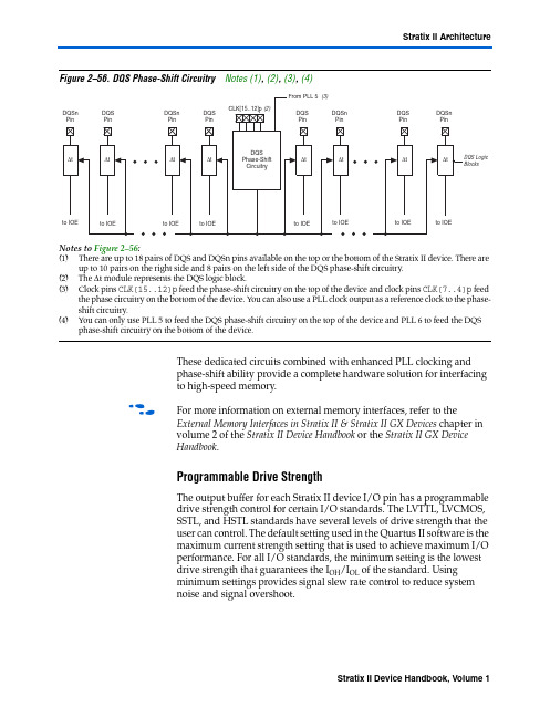
Stratix II Architecture Figure2–56.DQS Phase-Shift Circuitry Notes(1), (2), (3), (4)Notes to Figure2–56:(1)There are up to 18 pairs of DQS and DQSn pins available on the top or the bottom of the Stratix II device. There areup to 10 pairs on the right side and 8 pairs on the left side of the DQS phase-shift circuitry.(2)The Δt module represents the DQS logic block.(3)Clock pins CLK[15..12]p feed the phase-shift circuitry on the top of the device and clock pins CLK[7..4]p feedthe phase circuitry on the bottom of the device. You can also use a PLL clock output as a reference clock to the phase-shift circuitry.(4)You can only use PLL 5 to feed the DQS phase-shift circuitry on the top of the device and PLL 6 to feed the DQSphase-shift circuitry on the bottom of the device.These dedicated circuits combined with enhanced PLL clocking andphase-shift ability provide a complete hardware solution for interfacingto high-speed memory.f For more information on external memory interfaces, refer to theExternal Memory Interfaces in Stratix II & Stratix II GX Devices chapter involume 2 of the Stratix II Device Handbook or the Stratix II GX DeviceHandbook.Programmable Drive StrengthThe output buffer for each Stratix II device I/O pin has a programmabledrive strength control for certain I/O standards. The LVTTL, LVCMOS,SSTL, and HSTL standards have several levels of drive strength that theuser can control. The default setting used in the Quartus II software is themaximum current strength setting that is used to achieve maximum I/Operformance. For all I/O standards, the minimum setting is the lowestdrive strength that guarantees the I OH/I OL of the standard. Usingminimum settings provides signal slew rate control to reduce systemnoise and signal overshoot.High-Speed Differential I/O with DPA SupportHigh-Speed Differential I/O with DPA SupportStratix II devices contain dedicated circuitry for supporting differential standards at speeds up to 1 Gbps. The LVDS and HyperTransport differential I/O standards are supported in the Stratix II device. In addition, the LVPECL I/O standard is supported on input and output clock pins on the top and bottom I/O banks.The high-speed differential I/O circuitry supports the following high speed I/O interconnect standards and applications:■SPI-4 Phase 2 (POS-PHY Level 4)■SFI-4■Parallel RapidIO■HyperTransport technologyThere are four dedicated high-speed PLLs in the EP2S15 to EP2S30 devices and eight dedicated high-speed PLLs in the EP2S60 to EP2S180 devices to multiply reference clocks and drive high-speed differential SERDES channels.Tables 2–21 through 2–26 show the number of channels that each fast PLL can clock in each of the Stratix II devices. In Tables 2–21 through 2–26 the first row for each transmitter or receiver provides the number of channels driven directly by the PLL. The second row below it shows the maximum channels a PLL can drive if cross bank channels are used from theadjacent center PLL. For example, in the 484-pin FineLine BGA EP2S15Non-Stratix II VCC = 3.3 Vv (1)v (2)v (3)Level shifter required Level shifter required VCC = 2.5 V v (1), (4)v (2)v (3)Level shifter required Level shifter required VCC = 1.8 V v (1), (4)v (2), (5)v Level shifter requiredLevel shifter requiredVCC = 1.5 Vv (1), (4)v (2), (5)v (6)v vNotes to Table 2–20:(1)The TDO output buffer meets V OH (MIN) = 2.4 V .(2)The TDO output buffer meets V OH (MIN) = 2.0 V .(3)An external 250-Ω pull-up resistor is not required, but recommended if signal levels on the board are not optimal.(4)Input buffer must be 3.3-V tolerant.(5)Input buffer must be 2.5-V tolerant.(6)Input buffer must be 1.8-V tolerant.Table 2–20.Supported TDO/TDI Voltage Combinations (Part 2 of 2)DeviceTDI InputBuffer Power Stratix II TDO V C C I O Voltage Level in I/O Bank 4VC C I O = 3.3 V V C C I O = 2.5 V V C C I O = 1.8 V V C C I O = 1.5 V V C C I O = 1.2 VDocument Revision HistoryIEEE Std. 1149.1 JTAG Boundary-Scan SupportTable3–1.Stratix II JTAG InstructionsJTAG Instruction Instruction Code DescriptionSAMPLE/PRELOAD00 0000 0101Allows a snapshot of signals at the device pins to be captured andexamined during normal device operation, and permits an initialdata pattern to be output at the device pins. Also used by theSignalTap II embedded logic analyzer.EXTEST(1)00 0000 1111Allows the external circuitry and board-level interconnects to betested by forcing a test pattern at the output pins and capturing testresults at the input pins.BYPASS11 1111 1111Places the 1-bit bypass register between the TDI and TDO pins,which allows the BST data to pass synchronously through selecteddevices to adjacent devices during normal device operation. USERCODE00 0000 0111Selects the 32-bit USERCODE register and places it between theTDI and TDO pins, allowing the USERCODE to be serially shiftedout of TDO.IDCODE00 0000 0110Selects the IDCODE register and places it between TDI and TDO,allowing the IDCODE to be serially shifted out of TDO.HIGHZ (1)00 0000 1011Places the 1-bit bypass register between the TDI and TDO pins,which allows the BST data to pass synchronously through selecteddevices to adjacent devices during normal device operation, whiletri-stating all of the I/O pins.CLAMP (1)00 0000 1010Places the 1-bit bypass register between the TDI and TDO pins,which allows the BST data to pass synchronously through selecteddevices to adjacent devices during normal device operation whileholding I/O pins to a state defined by the data in the boundary-scanregister.ICR instructions Used when configuring a Stratix II device via the JT AG port with aUSB Blaster, MasterBlaster™, ByteBlasterMV™, or ByteBlaster IIdownload cable, or when using a .jam or .jbc via an embeddedprocessor or JRunner.PULSE_NCONFIG00 0000 0001Emulates pulsing the nCONFIG pin low to trigger reconfigurationeven though the physical pin is unaffected.CONFIG_IO (2)00 0000 1101Allows configuration of I/O standards through the JT AG chain forJT AG testing. Can be executed before, during, or afterconfiguration. Stops configuration if executed during configuration.Once issued, the CONFIG_IO instruction holds nSTATUS low toreset the configuration device. nSTATUS is held low until the IOEconfiguration register is loaded and the T AP controller statemachine transitions to the UPDATE_DR state.SignalTap II instructions Monitors internal device operation with the SignalTap II embedded logic analyzer.Notes to Table3–1:(1)Bus hold and weak pull-up resistor features override the high-impedance state of HIGHZ, CLAMP, and EXTEST.(2)For more information on using the CONFIG_IO instruction, see the MorphIO: An I/O Reconfiguration Solution forAltera Devices White Paper.Document Revision History。
M29F800DTM29F800DB8 Mbit (1Mb x8 or 512Kb x16, Boot Block)5V Supply Flash MemoryFEATURES SUMMARYs SUPPLY VOLTAGE Array–V CC =5V ±10% for Program, Erase and Reads ACCESS TIME: 55, 70, 90nss PROGRAMMING TIME–10µs per Byte/Word typicals19 MEMORY BLOCKS–1 Boot Block (Top or Bottom Location)–2 Parameter and 16 Main Blockss PROGRAM/ERASE CONTROLLER–Embedded Byte/Word Program algorithmss ERASE SUSPEND and RESUME MODES–Read and Program another Block duringErase Suspends UNLOCK BYPASS PROGRAM COMMAND–Faster Production/Batch Programmings TEMPORARY BLOCK UNPROTECTIONMODEs COMMON FLASH INTERFACE–64 bit Security Codes LOW POWER CONSUMPTION–Standby and Automatic Standbys100,000 PROGRAM/ERASE CYCLES perBLOCKs ELECTRONIC SIGNATURE–Manufacturer Code: 0020h–Top Device Code M29F800DT: 22ECh–Bottom Device Code M29F800DB: 2258hFebruary 20031/39M29F800DT, M29F800DBTABLE OF CONTENTSSUMMARY DESCRIPTION. . . . . . . . . . . . . . . . . . . . . . . . . . . . . . . . . . . . . . . . . . . . . . . . . . . . . . . . . . .5Figure 2. Logic Diagram . . . . . . . . . . . . . . . . . . . . . . . . . . . . . . . . . . . . . . . . . . . . . . . . . . . . . . . . . .5 Table 1. Signal Names . . . . . . . . . . . . . . . . . . . . . . . . . . . . . . . . . . . . . . . . . . . . . . . . . . . . . . . . . . .5 Figure 3. SO Connections. . . . . . . . . . . . . . . . . . . . . . . . . . . . . . . . . . . . . . . . . . . . . . . . . . . . . . . . .6 Figure 4. TSOP Connections. . . . . . . . . . . . . . . . . . . . . . . . . . . . . . . . . . . . . . . . . . . . . . . . . . . . . . .6 Figure 5. Block Addresses (x8). . . . . . . . . . . . . . . . . . . . . . . . . . . . . . . . . . . . . . . . . . . . . . . . . . . . .7 Figure 6. Block Addresses (x16). . . . . . . . . . . . . . . . . . . . . . . . . . . . . . . . . . . . . . . . . . . . . . . . . . . .8SIGNAL DESCRIPTIONS. . . . . . . . . . . . . . . . . . . . . . . . . . . . . . . . . . . . . . . . . . . . . . . . . . . . . . . . . . . .9Address Inputs (A0-A18). . . . . . . . . . . . . . . . . . . . . . . . . . . . . . . . . . . . . . . . . . . . . . . . . . . . . . . . . .9 Data Inputs/Outputs (DQ0-DQ7). . . . . . . . . . . . . . . . . . . . . . . . . . . . . . . . . . . . . . . . . . . . . . . . . . . .9 Data Inputs/Outputs (DQ8-DQ14). . . . . . . . . . . . . . . . . . . . . . . . . . . . . . . . . . . . . . . . . . . . . . . . . . .9 Data Input/Output or Address Input (DQ15A-1).. . . . . . . . . . . . . . . . . . . . . . . . . . . . . . . . . . . . . . . .9 Chip Enable (E). . . . . . . . . . . . . . . . . . . . . . . . . . . . . . . . . . . . . . . . . . . . . . . . . . . . . . . . . . . . . . . . .9 Output Enable (G). . . . . . . . . . . . . . . . . . . . . . . . . . . . . . . . . . . . . . . . . . . . . . . . . . . . . . . . . . . . . . .9 Write Enable (W). . . . . . . . . . . . . . . . . . . . . . . . . . . . . . . . . . . . . . . . . . . . . . . . . . . . . . . . . . . . . . . .9 Reset/Block Temporary Unprotect (RP).. . . . . . . . . . . . . . . . . . . . . . . . . . . . . . . . . . . . . . . . . . . . . .9 Ready/Busy Output (RB). . . . . . . . . . . . . . . . . . . . . . . . . . . . . . . . . . . . . . . . . . . . . . . . . . . . . . . . . .9 Byte/Word Organization Select (BYTE). . . . . . . . . . . . . . . . . . . . . . . . . . . . . . . . . . . . . . . . . . . . . ..9 V CC Supply Voltage. . . . . . . . . . . . . . . . . . . . . . . . . . . . . . . . . . . . . . . . . . . . . . . . . . . . . . . . . . . . . .9 VSS Ground.. . . . . . . . . . . . . . . . . . . . . . . . . . . . . . . . . . . . . . . . . . . . . . . . . . . . . . . . . . . . . . . . . . .9BUS OPERATIONS. . . . . . . . . . . . . . . . . . . . . . . . . . . . . . . . . . . . . . . . . . . . . . . . . . . . . . . . . . . . . . . .10Bus Read. . . . . . . . . . . . . . . . . . . . . . . . . . . . . . . . . . . . . . . . . . . . . . . . . . . . . . . . . . . . . . . . . . . . .10 Bus Write. . . . . . . . . . . . . . . . . . . . . . . . . . . . . . . . . . . . . . . . . . . . . . . . . . . . . . . . . . . . . . . . . . . . .10 Output Disable. . . . . . . . . . . . . . . . . . . . . . . . . . . . . . . . . . . . . . . . . . . . . . . . . . . . . . . . . . . . . . . . .10 Standby. . . . . . . . . . . . . . . . . . . . . . . . . . . . . . . . . . . . . . . . . . . . . . . . . . . . . . . . . . . . . . . . . . . . . .10 Automatic Standby.. . . . . . . . . . . . . . . . . . . . . . . . . . . . . . . . . . . . . . . . . . . . . . . . . . . . . . . . . . . . .10 Special Bus Operations. . . . . . . . . . . . . . . . . . . . . . . . . . . . . . . . . . . . . . . . . . . . . . . . . . . . . . . . . .10 Electronic Signature.. . . . . . . . . . . . . . . . . . . . . . . . . . . . . . . . . . . . . . . . . . . . . . . . . . . . . . . . . . . .10 Block Protection and Blocks Unprotection. . . . . . . . . . . . . . . . . . . . . . . . . . . . . . . . . . . . . . . . . . . .10 Table 2. Bus Operations, BYTE = V IL . . . . . . . . . . . . . . . . . . . . . . . . . . . . . . . . . . . . . . . . . . . . . . .10 Table 3. Bus Operations, BYTE = V IH. . . . . . . . . . . . . . . . . . . . . . . . . . . . . . . . . . . . . . . . . . . . . . .11COMMAND INTERFACE . . . . . . . . . . . . . . . . . . . . . . . . . . . . . . . . . . . . . . . . . . . . . . . . . . . . . . . . . . .11Read/Reset Command.. . . . . . . . . . . . . . . . . . . . . . . . . . . . . . . . . . . . . . . . . . . . . . . . . . . . . . . . . .11 Auto Select Command. . . . . . . . . . . . . . . . . . . . . . . . . . . . . . . . . . . . . . . . . . . . . . . . . . . . . . . . . . .11 Program Command. . . . . . . . . . . . . . . . . . . . . . . . . . . . . . . . . . . . . . . . . . . . . . . . . . . . . . . . . . . . .11 Unlock Bypass Command. . . . . . . . . . . . . . . . . . . . . . . . . . . . . . . . . . . . . . . . . . . . . . . . . . . . . . . .12 Unlock Bypass Program Command.. . . . . . . . . . . . . . . . . . . . . . . . . . . . . . . . . . . . . . . . . . . . . . . .12 Unlock Bypass Reset Command. . . . . . . . . . . . . . . . . . . . . . . . . . . . . . . . . . . . . . . . . . . . . . . . . . .12 Chip Erase Command. . . . . . . . . . . . . . . . . . . . . . . . . . . . . . . . . . . . . . . . . . . . . . . . . . . . . . . . . . .12 Block Erase Command.. . . . . . . . . . . . . . . . . . . . . . . . . . . . . . . . . . . . . . . . . . . . . . . . . . . . . . . . . .12 Erase Suspend Command.. . . . . . . . . . . . . . . . . . . . . . . . . . . . . . . . . . . . . . . . . . . . . . . . . . . . . . .12 Erase Resume Command. . . . . . . . . . . . . . . . . . . . . . . . . . . . . . . . . . . . . . . . . . . . . . . . . . . . . . . .132/39M29F800DT, M29F800DBRead CFI Query Command. . . . . . . . . . . . . . . . . . . . . . . . . . . . . . . . . . . . . . . . . . . . . . . . . . . . . . .13 Block Protect and Chip Unprotect Commands.. . . . . . . . . . . . . . . . . . . . . . . . . . . . . . . . . . . . . . . .13 Table 4. Commands, 16-bit mode, BYTE = V IH . . . . . . . . . . . . . . . . . . . . . . . . . . . . . . . . . . . . . . .14 Table 5. Commands, 8-bit mode, BYTE = V IL. . . . . . . . . . . . . . . . . . . . . . . . . . . . . . . . . . . . . . . . .15 Table 6. Program, Erase Times and Program, Erase Endurance Cycles. . . . . . . . . . . . . . . . . . . .15STATUS REGISTER. . . . . . . . . . . . . . . . . . . . . . . . . . . . . . . . . . . . . . . . . . . . . . . . . . . . . . . . . . . . . . .16Data Polling Bit (DQ7). . . . . . . . . . . . . . . . . . . . . . . . . . . . . . . . . . . . . . . . . . . . . . . . . . . . . . . . . . .16 Toggle Bit (DQ6).. . . . . . . . . . . . . . . . . . . . . . . . . . . . . . . . . . . . . . . . . . . . . . . . . . . . . . . . . . . . . . .16 Error Bit (DQ5). . . . . . . . . . . . . . . . . . . . . . . . . . . . . . . . . . . . . . . . . . . . . . . . . . . . . . . . . . . . . . . . .16 Erase Timer Bit (DQ3). . . . . . . . . . . . . . . . . . . . . . . . . . . . . . . . . . . . . . . . . . . . . . . . . . . . . . . . . . .16 Alternative Toggle Bit (DQ2).. . . . . . . . . . . . . . . . . . . . . . . . . . . . . . . . . . . . . . . . . . . . . . . . . . . . . .16 Table 7. Status Register Bits. . . . . . . . . . . . . . . . . . . . . . . . . . . . . . . . . . . . . . . . . . . . . . . . . . . . . .17 Figure 7. Data Polling Flowchart. . . . . . . . . . . . . . . . . . . . . . . . . . . . . . . . . . . . . . . . . . . . . . . . . . .17 Figure 8. Data Toggle Flowchart. . . . . . . . . . . . . . . . . . . . . . . . . . . . . . . . . . . . . . . . . . . . . . . . . . .17MAXIMUM RATING. . . . . . . . . . . . . . . . . . . . . . . . . . . . . . . . . . . . . . . . . . . . . . . . . . . . . . . . . . . . . . . .18 Table 8. Absolute Maximum Ratings. . . . . . . . . . . . . . . . . . . . . . . . . . . . . . . . . . . . . . . . . . . . . . . .18 DC and AC PARAMETERS . . . . . . . . . . . . . . . . . . . . . . . . . . . . . . . . . . . . . . . . . . . . . . . . . . . . . . . . .19Table 9. Operating and AC Measurement Conditions. . . . . . . . . . . . . . . . . . . . . . . . . . . . . . . . . . .19 Figure 9. AC Measurement I/O Waveform . . . . . . . . . . . . . . . . . . . . . . . . . . . . . . . . . . . . . . . . . . .19 Figure 10. AC Measurement Load Circuit. . . . . . . . . . . . . . . . . . . . . . . . . . . . . . . . . . . . . . . . . . . .19 Table 10. Device Capacitance. . . . . . . . . . . . . . . . . . . . . . . . . . . . . . . . . . . . . . . . . . . . . . . . . . . . .19 Table 11. DC Characteristics. . . . . . . . . . . . . . . . . . . . . . . . . . . . . . . . . . . . . . . . . . . . . . . . . . . . . .20 Figure 11. Read Mode AC Waveforms . . . . . . . . . . . . . . . . . . . . . . . . . . . . . . . . . . . . . . . . . . . . . .21 Table 12. Read AC Characteristics. . . . . . . . . . . . . . . . . . . . . . . . . . . . . . . . . . . . . . . . . . . . . . . . .21 Figure 12. Write AC Waveforms, Write Enable Controlled . . . . . . . . . . . . . . . . . . . . . . . . . . . . . . .22 Table 13. Write AC Characteristics, Write Enable Controlled. . . . . . . . . . . . . . . . . . . . . . . . . . . . .22 Figure 13. Write AC Waveforms, Chip Enable Controlled. . . . . . . . . . . . . . . . . . . . . . . . . . . . . . . .23 Table 14. Write AC Characteristics, Chip Enable Controlled . . . . . . . . . . . . . . . . . . . . . . . . . . . . .23 Figure 14. Reset/Block Temporary Unprotect AC Waveforms . . . . . . . . . . . . . . . . . . . . . . . . . . . .24 Table 15. Reset/Block Temporary Unprotect AC Characteristics . . . . . . . . . . . . . . . . . . . . . . . . . .24PACKAGE MECHANICAL . . . . . . . . . . . . . . . . . . . . . . . . . . . . . . . . . . . . . . . . . . . . . . . . . . . . . . . . . .25Figure 15. SO44 - 44 lead Plastic Small Outline, 525 mils body width, Package Outline. . . . . . . .25 Table 16. SO44 – 44 lead Plastic Small Outline, 525 mils body width, Package Mechanical Data25 Figure 16. TSOP48 – 48 lead Plastic Thin Small Outline, 12 x 20mm, Package Outline . . . . . . . .26 Table 17. TSOP48 – 48 lead Plastic Thin Small Outline, 12 x 20mm, Package Mechanical Data .26PART NUMBERING . . . . . . . . . . . . . . . . . . . . . . . . . . . . . . . . . . . . . . . . . . . . . . . . . . . . . . . . . . . . . . .27 Table 18. Ordering Information Scheme. . . . . . . . . . . . . . . . . . . . . . . . . . . . . . . . . . . . . . . . . . . . .27APPENDIX A. BLOCK ADDRESS TABLE. . . . . . . . . . . . . . . . . . . . . . . . . . . . . . . . . . . . . . . . . . . . . .28Table 19. Top Boot Block Addresses, M29F800DT . . . . . . . . . . . . . . . . . . . . . . . . . . . . . . . . . . . .28 Table 20. Bottom Boot Block Addresses, M29F800DB. . . . . . . . . . . . . . . . . . . . . . . . . . . . . . . . . .283/39M29F800DT, M29F800DBAPPENDIX B. COMMON FLASH INTERFACE (CFI) . . . . . . . . . . . . . . . . . . . . . . . . . . . . . . . . . . . . .29Table 21. Query Structure Overview. . . . . . . . . . . . . . . . . . . . . . . . . . . . . . . . . . . . . . . . . . . . . . ..29 Table 22. CFI Query Identification String . . . . . . . . . . . . . . . . . . . . . . . . . . . . . . . . . . . . . . . . . . ..29 Table 23. CFI Query System Interface Information. . . . . . . . . . . . . . . . . . . . . . . . . . . . . . . . . . . . .30 Table 24. Device Geometry Definition. . . . . . . . . . . . . . . . . . . . . . . . . . . . . . . . . . . . . . . . . . . . . ..31 Table 25. Primary Algorithm-Specific Extended Query Table. . . . . . . . . . . . . . . . . . . . . . . . . . . . .32 Table 25. Primary Algorithm-Specific Extended Query Table. . . . . . . . . . . . . . . . . . . . . . . . . . . . .32APPENDIX C. BLOCK PROTECTION . . . . . . . . . . . . . . . . . . . . . . . . . . . . . . . . . . . . . . . . . . . . . . . . .33 Programmer Technique . . . . . . . . . . . . . . . . . . . . . . . . . . . . . . . . . . . . . . . . . . . . . . . . . . . . . . . .33In-System Technique . . . . . . . . . . . . . . . . . . . . . . . . . . . . . . . . . . . . . . . . . . . . . . . . . . . . . . . . . .33 Table 27. Programmer Technique Bus Operations, BYTE = V IH or V IL . . . . . . . . . . . . . . . . . . . . .33 Figure 17. Programmer Equipment Block Protect Flowchart . . . . . . . . . . . . . . . . . . . . . . . . . . . . .34 Figure 18. Programmer Equipment Chip Unprotect Flowchart . . . . . . . . . . . . . . . . . . . . . . . . . . . .35 Figure 19. In-System Equipment Block Protect Flowchart . . . . . . . . . . . . . . . . . . . . . . . . . . . . . . .36 Figure 20. In-System Equipment Chip Unprotect Flowchart. . . . . . . . . . . . . . . . . . . . . . . . . . . . . .37REVISION HISTORY. . . . . . . . . . . . . . . . . . . . . . . . . . . . . . . . . . . . . . . . . . . . . . . . . . . . . . . . . . . . . . .38 Table 28. Document Revision History. . . . . . . . . . . . . . . . . . . . . . . . . . . . . . . . . . . . . . . . . . . . . . .384/39M29F800DT, M29F800DB SUMMARY DESCRIPTIONThe M29F800D is a 8 Mbit (1Mb x8 or 512Kb x16) non-volatile memory that can be read, erased and reprogrammed. These operations can be per-formed using a single low voltage (5V) supply. On power-up the memory defaults to its Read mode where it can be read in the same way as a ROM or EPROM.The memory is divided into blocks that can be erased independently so it is possible to preserve valid data while old data is erased. Each block can be protected independently to prevent accidental Program or Erase commands from modifying the memory. Program and Erase commands are writ-ten to the Command Interface of the memory. An on-chip Program/Erase Controller simplifies the process of programming or erasing the memory by taking care of all of the special operations that are required to update the memory contents.The end of a program or erase operation can be detected and any error conditions identified. The command set required to control the memory is consistent with JEDEC standards.The blocks in the memory are asymmetrically ar-ranged, see Figures 5 and 6, Block Addresses. The first or last 64 Kbytes have been divided into four additional blocks. The 16 Kbyte Boot Block can be used for small initialization code to start the microprocessor, the two 8 Kbyte Parameter Blocks can be used for parameter storage and the remaining 32K is a small Main Block where the ap-plication may be stored.Chip Enable, Output Enable and Write Enable sig-nals control the bus operation of the memory. They allow simple connection to most micropro-cessors, often without additional logic.The memory is offered in SO44 and TSOP48 (12 x 20mm) packages. The memory is supplied with all the bits erased (set to ’1’).Table 1. Signal NamesA0-A18Address InputsDQ0-DQ7Data Inputs/OutputsDQ8-DQ14Data Inputs/OutputsDQ15A–1Data Input/Output or Address InputE Chip EnableG Output EnableW Write EnableRP Reset/Block Temporary UnprotectRBReady/Busy Output(not available on SO44 package) BYTE Byte/Word Organization SelectV CC Supply VoltageV SS GroundNC Not Connected Internally5/39M29F800DT, M29F800DB6/39M29F800DT, M29F800DB7/39M29F800DT, M29F800DB8/39M29F800DT, M29F800DB SIGNAL DESCRIPTIONSSee Figure 2, Logic Diagram, and Table 1, Signal Names, for a brief overview of the signals connect-ed to this device.Address Inputs (A0-A18).The Address Inputs select the cells in the memory array to access dur-ing Bus Read operations. During Bus Write opera-tions they control the commands sent to the Command Interface of the internal state machine. Data Inputs/Outputs (DQ0-DQ7).The Data In-puts/Outputs output the data stored at the selected address during a Bus Read operation. During Bus Write operations they represent the commands sent to the Command Interface of the internal state machine.Data Inputs/Outputs (DQ8-DQ14).The Data In-puts/Outputs output the data stored at the selected address during a Bus Read operation when BYTE is High, V IH IL, these pins are not used and are high impedance. During Bus Write operations the Command Register does not use these bits. When reading the Status Register these bits should be ignored.Data Input/Output or Address Input (DQ15A-1). When BYTE is High, V IH, this pin behaves as a Data Input/Output pin (as DQ8-DQ14). WhenIL, this pin behaves as an address pin; DQ15A–1 Low will select the LSB of the Word on the other addresses, DQ15A–1 High will select the MSB. Throughout the text consider references to the Data Input/Output to include this pin when BYTE is High and references to the Address In-when stated explicitly otherwise.the memory, allowing Bus Read and Bus Write op-erations to be performed. When Chip Enable is High, V IH, all other pins are ignored.trols the Bus Read operation of the memory.the Bus Write operation of the memory’s Com-mand Interface.The Reset/Block Temporary Unprotect pin can be used to apply a Hardware Reset to the memory or to temporarily unprotect all Blocks that have been protected.A Hardware Reset is achieved by holding Reset/ Block Temporary Unprotect Low, V IL, for at least t PLPX. After Reset/Block Temporary Unprotect goes High, V IH, the memory will be ready for Bus Read and Bus Write operations after t PHEL or t RHEL, whichever occurs last. See the Ready/Busy Output section, Table 15 and Figure 14, Reset/ Temporary Unprotect AC Characteristics for more details.Holding RP at V ID will temporarily unprotect the protected Blocks in the memory. Program and Erase operations on all blocks will be possible. The transition from V IH to V ID must be slower than t PHPHH.Ready/Busy Output (RB).The Ready/Busy pin is an open-drain output that can be used to identify when the device is performing a Program or Erase operation. During Program or Erase operations Ready/Busy is Low, V OL. Ready/Busy is high-im-pedance during Read mode, Auto Select mode and Erase Suspend mode.After a Hardware Reset, Bus Read and Bus Write operations cannot begin until Ready/Busy be-comes high-impedance. See Table 15 and Figure 14, Reset/Temporary Unprotect AC Characteris-tics.The use of an open-drain output allows the Ready/ Busy pins from several memories to be connected to a single pull-up resistor. A Low will then indicate that one, or more, of the memories is busy.The Byte/Word Organization Select pin is used to switch between the 8-bit and 16-bit Bus modes of the memory. When Byte/Word Organization Se-lect is Low, V IL, the memory is in 8-bit mode, when it is High, V IH, the memory is in 16-bit mode.V CC Supply Voltage.The V CC Supply Voltage supplies the power for all operations (Read, Pro-gram, Erase etc.).The Command Interface is disabled when the V CC Supply Voltage is less than the Lockout Voltage, V LKO. This prevents Bus Write operations from ac-cidentally damaging the data during power up, power down and power surges. If the Program/ Erase Controller is programming or erasing during this time then the operation aborts and the memo-ry contents being altered will be invalid.A 0.1µF capacitor should be connected between the V CC Supply Voltage pin and the V SS Ground pin to decouple the current surges from the power supply. The PCB track widths must be sufficient to carry the currents required during program and erase operations, I CC3.V SS Ground.The V SS Ground is the reference for all voltage measurements.9/39M29F800DT, M29F800DB10/39BUS OPERATIONSThere are five standard bus operations that control the device. These are Bus Read, Bus Write, Out-put Disable, Standby and Automatic Standby. See Tables 2 and 3, Bus Operations, for a summary.Typically glitches of less than 5ns on Chip Enable or Write Enable are ignored by the memory and do not affect bus operations.Bus Read.Bus Read operations read from the memory cells, or specific registers in the Com-mand Interface. A valid Bus Read operation in-volves setting the desired address on the Address Inputs, applying a Low signal, V IL , to Chip Enable and Output Enable and keeping Write Enable High, V IH . The Data Inputs/Outputs will output the value, see Figure 11, Read Mode AC Waveforms,and Table 12, Read AC Characteristics, for details of when the output becomes valid.Bus Write.Bus Write operations write to the Command Interface. A valid Bus Write operation begins by setting the desired address on the Ad-dress Inputs. The Address Inputs are latched by the Command Interface on the falling edge of Chip Enable or Write Enable, whichever occurs last.The Data Inputs/Outputs are latched by the Com-mand Interface on the rising edge of Chip Enable or Write Enable, whichever occurs first. Output En-able must remain High, V IH , during the whole Bus Write operation. See Figures 12 and 13, Write AC Waveforms, and Tables 13 and 14, Write AC Characteristics, for details of the timing require-ments.Output Disable.The Data Inputs/Outputs are in the high impedance state when Output Enable is High, V IH .Standby.When Chip Enable is High, V IH , the memory enters Standby mode and the Data In-puts/Outputs pins are placed in the high-imped-ance state. To reduce the Supply Current to the Standby Supply Current, I CC2, Chip Enable should be held within V CC ± 0.2V. For the Standby current level see Table 11, DC Characteristics.During program or erase operations the memory will continue to use the Program/Erase Supply Current, I CC3, for Program or Erase operations un-til the operation completes.Automatic Standby.If CMOS levels (V CC ± 0.2V)are used to drive the bus and the bus is inactive for 150ns or more the memory enters Automatic Standby where the internal Supply Current is re-duced to the Standby Supply Current, I CC2. The Data Inputs/Outputs will still output data if a Bus Read operation is in progress.Special Bus Operations.Additional bus opera-tions can be performed to read the Electronic Sig-nature and also to apply and remove Block Protection. These bus operations are intended for use by programming equipment and are not usu-ally used in applications. They require V ID to be applied to some pins.Electronic Signature.The memory has two codes, the manufacturer code and the device code, that can be read to identify the memory.These codes can be read by applying the signals listed in Tables 2 and 3, Bus Operations.Block Protection and Blocks Unprotection.Each block can be separately protected against accidental Program or Erase. Protected blocks can be unprotected to allow data to be changed. There are two methods available for protecting and unprotecting the blocks, one for use on pro-gramming equipment and the other for in-system use. Block Protect and Chip Unprotect operations are described in Appendix C.ILNote:X = V IL or V IH .Operation E G W Address Inputs DQ15A–1, A0-A18Data Inputs/Outputs DQ14-DQ8DQ7-DQ0Bus Read V IL V IL V IH Cell Address Hi-Z Data Output Bus Write V IL V IH V IL Command Address Hi-Z Data Input Output Disable X V IH V IH X Hi-Z Hi-Z StandbyV IH X X XHi-Z Hi-Z Read Manufacturer CodeV IL V IL V IH A0 = V IL , A1 = V IL , A9 = V ID , Others V IL or V IHHi-Z 20hRead Device CodeV ILV ILV IHA0 = V IH , A1 = V IL , A9 = V ID , Others V IL or V IHHi-ZECh (M29F800DT)58h (M29F800DB)Table 3. Bus Operations, BYTE = V IHNote:X = V IL or V IH.COMMAND INTERFACEAll Bus Write operations to the memory are inter-preted by the Command Interface. Commands consist of one or more sequential Bus Write oper-ations. Failure to observe a valid sequence of Bus Write operations will result in the memory return-ing to Read mode. The long command sequences are imposed to maximize data security.The address used for the commands changes de-pending on whether the memory is in 16-bit or 8-bit mode. See either Table 4, or 5, depending on the configuration that is being used, for a summary of the commands.Read/Reset Command.The Read/Reset com-mand returns the memory to its Read mode where it behaves like a ROM or EPROM, unless other-wise stated. It also resets the errors in the Status Register. Either one or three Bus Write operations can be used to issue the Read/Reset command. The Read/Reset Command can be issued, be-tween Bus Write cycles before the start of a pro-gram or erase operation, to return the device to read mode. Once the program or erase operation has started the Read/Reset command is no longer accepted. The Read/Reset command will not abort an Erase operation when issued while in Erase Suspend.Auto Select Command.The Auto Select com-mand is used to read the Manufacturer Code, the Device Code and the Block Protection Status. Three consecutive Bus Write operations are re-quired to issue the Auto Select command. Once the Auto Select command is issued the memory remains in Auto Select mode until a Read/Reset command is issued. Read CFI Query and Read/ Reset commands are accepted in Auto Select mode, all other commands are ignored.From the Auto Select mode the Manufacturer Code can be read using a Bus Read operation with A0 = V IL and A1 = V IL. The other address bits may be set to either V IL or V IH. The Manufacturer Code for STMicroelectronics is 0020h.The Device Code can be read using a Bus Read operation with A0 = V IH and A1 = V IL. The other address bits may be set to either V IL or V IH.The Block Protection Status of each block can be read using a Bus Read operation with A0 = V IL, A1=V IH, and A12-A18 specifying the address of the block. The other address bits may be set to ei-ther V IL or V IH. If the addressed block is protected then 01h is output on Data Inputs/Outputs DQ0-DQ7, otherwise 00h is output.Program Command.The Program command can be used to program a value to one address in the memory array at a time. The command re-quires four Bus Write operations, the final write op-eration latches the address and data in the internal state machine and starts the Program/Erase Con-troller.If the address falls in a protected block then the Program command is ignored, the data remains unchanged. The Status Register is never read and no error condition is given.During the program operation the memory will ig-nore all commands. It is not possible to issue any command to abort or pause the operation. Typical program times are given in Table 6. Bus Read op-erations during the program operation will output the Status Register on the Data Inputs/Outputs. See the section on the Status Register for more details.After the program operation has completed the memory will return to the Read mode, unless an error has occurred. When an error occurs theOperation E G W Address InputsA0-A18Data Inputs/OutputsDQ15A–1, DQ14-DQ0Bus Read V IL V IL V IH Cell Address Data Output Bus Write V IL V IH V IL Command Address Data Input Output Disable X V IH V IH X Hi-Z Standby V IH X X X Hi-ZRead Manufacturer Code V IL V IL V IHA0 = V IL, A1 = V IL, A9 = V ID,Others V IL or V IH0020hRead Device Code V IL V IL V IH A0 = V IH, A1 = V IL, A9 = V ID,Others V IL or V IH22ECh (M29F800DT)2258h (M29F800DB)。