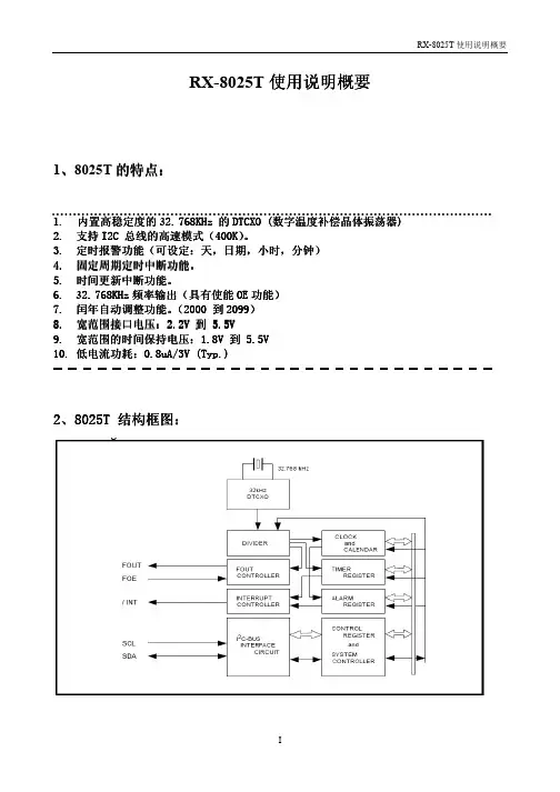
RX-8025T规格书(中文)
- 格式:pdf
- 大小:435.80 KB
- 文档页数:1


Features Array•Pin and Software Compatibility with Standard 80C51 Products and 80C51Fx/Rx/Rx+•Plug-In Replacement of Intel’s 8xC251Sx•C251 Core: Intel’s MCS®251 D-step Compliance•40-byte Register File•Registers Accessible as Bytes, Words or Dwords•Three-stage Instruction Pipeline•16-bit Internal Code Fetch•Enriched C51 Instruction Set•16-bit and 32-bit ALU•Compare and Conditional Jump Instructions•Expanded Set of Move Instructions•Linear Addressing• 1 Kbyte of On-Chip RAM•External Memory Space (Code/Data) Programmable from 64 kilobytes to 256 kilobytes •TSC87251G2D: 32 kilobytes of On-Chip EPROM/OTPROM–SINGLE PULSE Programming Algorithm•TSC83251G2D: 32 kilobytes of On-Chip Masked ROM•TSC80251G2D: ROMless Version•Four 8-bit Parallel I/O Ports (Ports 0, 1, 2 and 3 of the Standard 80C51)•Serial I/O Port: Full Duplex UART (80C51 Compatible) With Independent Baud Rate Generator•SSLC: Synchronous Serial Link Controller•TWI Multi-master Protocol•μWire and SPI Master and Slave Protocols•Three 16-bit Timers/Counters (Timers 0, 1 and 2 of the Standard 80C51)•EWC: Event and Waveform Controller•Compatible with Intel’s Programmable Counter Array (PCA)•Common 16-bit Timer/Counter Reference with Four Possible Clock Sources (Fosc/4, Fosc/12, Timer 1 and External Input)•Five Modules, Each with Four Programmable Modes:–16-bit Software Timer/Counter–16-bit Timer/Counter Capture Input and Software Pulse Measurement–High-speed Output and 16-bit Software Pulse Width Modulation (PWM)–8-bit Hardware PWM Without Overhead•16-bit Watchdog Timer/Counter Capability•Secure 14-bit Hardware Watchdog Timer•Power Management•Power-On Reset (Integrated on the Chip)•Power-Off Flag (Cold and Warm Resets)•Software Programmable System Clock•Idle Mode•Power-down Mode•Keyboard Interrupt Interface on Port 1•Non Maskable Interrupt Input (NMI)•Real-Time Wait States Inputs (WAIT#/AWAIT#)•ONCE Mode and Full Speed Real-time In-circuit Emulation Support (Third Party Vendors)•High Speed Versions:–4.5V to 5.5V–16 MHz and 24 MHz•Typical Operating Current: 35 mA at 24 MHz24 mA at 16 MHz•Typical Power-down Current: 2 μA•Low Voltage Version:–2.7V to 5.5V–16MHz•Typical Operating Current:11 mA at 3V•Typical Power-down Current: 1 μA•Temperature Ranges: Commercial (0°C to +70°C), Industrial (-40°C to +85°C), Automotive ((-40°C to +85°C) ROM only)•Option: Extended Range (-55°C to +125°C)•Packages: PDIL 40, PLCC 44 and VQFP 44•Options: Known Good Dice and Ceramic PackagesDescriptionThe TSC80251G2D products are derivatives of the Atmel Microcontroller family based on the 8/16-bit C251 Architecture. This family of products is tailored to 8/16-bit microcontroller applications requiring an increased instruction throughput, a reduced operating frequency or a larger addressable memory space. The architecture can provide a significant code size reduction when compiling C programs while fully preserving the legacy of C51 assembly routines.The TSC80251G2D derivatives are pin and software compatible with standard 80C51/Fx/Rx/Rx+ with extended on-chip data memory (1Kbyte RAM) and up to 256kilobytes of external code and data. Additionally, the TSC83251G2D and TSC87251G2D provide on-chip code memory: 32 kilobytes ROM and 32 kilobytes EPROM/OTPROM respectively.They provide transparent enhancements to Intel’s 8xC251Sx family with an additional Synchronous Serial Link Controller (SSLC supporting TWI, μWire and SPI protocols), a Keyboard interrupt interface, a dedicated Baud Rate Generator for UART, and Power Management features.TSC80251G2D derivatives are optimized for speed and for low power consumption on a wide voltage range.Note: 1.This Datasheet provides the technical description of the TSC80251G2D derivatives. For further information on the device usage, please request the TSC80251 Programmer’s Guide and the TSC80251G1D Design Guide and errata sheet. Typical Applications•ISDN Terminals•High-Speed Modems•PABX (SOHO)•Line Cards•DVD ROM and Players•Printers•Plotters•Scanners•Banking Machines•Barcode Readers•Smart Cards Readers•High-End Digital Monitors•High-End Joysticks•High-end TV’s2AT/TSC8x251G2DAT/TSC8x251G2DBlock Diagram16-bit Memory Code16-bit Memory Address16-b i t I n s t r u c t i o n B u s24-b i t P r o g r a m C o u n t e r B u s8-b i t D a t a B u s24-b i t D a t a A d d r e s s B u s8-b i t I n t e r n a l B u sP e r i p h e r a l I n t e r f a c e U n i tVDD VSS VSS1P3(A16)P1(A17)P2(A15-8)P0(AD7-0)RSTXTAL2XTAL1NMIEA#/VPPALE/PROG#PSEN#Timers 0, 1 and 2Event and WaveformControllerTWI/SPI/m Wire ControllerWatchdog TimerPower ManagementClock UnitClock System PrescalerKeyboard InterfaceBus Interface UnitCPUPORTS 0-3Interrupt HandlerUnitRAM 1 KbyteROM UARTBaud Rate GeneratorAWAIT#EPROM OTPROM 32 KBVSS24AT/TSC8x251G2DPin DescriptionPinoutFigure 1. TSC80251G2D 40-pin DIP packageFigure 2. TSC80251G2D 44-pin PLCC PackageTSC80251G2D78910111213141615171819201234563433323130292827252624232221403938373635P1.5/CEX2/MISOP1.6/CEX3/SCL/SCK/WAIT#P1.7/A17/CEX4/SDA/MOSI/WCLKRST P3.0/RXD P3.1/TXD P3.2/INT0#P3.3/INT1#P3.4/T0P3.5/T1P1.4/CEX1/SS#P1.3/CEX0P1.2/ECI P1.1/T2EX P1.0/T2VDDP0.0/AD0P0.1/AD1P0.2/AD2P0.3/AD3P0.4/AD4P0.5/AD5P0.6/AD6P0.7/AD7EA#/VPP PSEN#ALE/PROG#P2.7/A15P2.6/A14P2.5/A13P3.7/A16/RD#XTAL2XTAL1VSSP2.0/A8P2.1/A9P2.2/A10P2.3/A11P2.4/A12P3.6/WR#TSC80251G2DP 1.4/C E X 1/S S #P 1.3/C E X 0P 1.2/E C I P 1.1/T 2E X P 1.0/T 2V S S 1V D D P 0.0/A D 0P 0.1/A D 1P 0.2/A D 2P 0.3/A D 3P 3.7/A 16/R D #X T A L 2X T A L 1V S S V S S 2P 2.0/A 8P 2.1/A 9P 2.2/A 10P 2.3/A 11P 2.4/A 12P 3.6/W R #393837363534333229303178910111213141716151819202122232425262728654324443424140P0.4/AD4P0.5/AD5P0.6/AD6P0.7/AD7EA#/VPP PSEN#ALE/PROG#NMIP2.7/A15P2.6/A14P2.5/A13P1.5/CEX2/MISOP1.6/CEX3/SCL/SCK/WAIT#P1.7/A17/CEX4/SDA/MOSI/WCLKRST P3.0/RXD AWAIT#P3.1/TXD P3.2/INT0#P3.3/INT1#P3.4/T0P3.5/T11AT/TSC8x251G2DFigure 3. TSC80251G2D 44-pin VQFP PackageTSC80251G2DP 1.4/C E X 1/S S #P 1.3/C E X 0P 1.2/E C I P 1.1/T 2E X P 1.0/T 2V S S 1V D D P 0.0/A D 0P 0.1/A D 1P 0.2/A D 2P 0.3/A D 3P 3.7/A 16/R D #X T A L 2X T A L 1V S S V S S 2P 2.0/A 8P 2.1/A 9P 2.2/A 10P 2.3/A 11P 2.4/A 12P 3.6/W R #3332313029282726232425123456781110912131415161718192021224443424140393837363534P0.4/AD4P0.5/AD5P0.6/AD6P0.7/AD7EA#/VPP PSEN#ALE/PROG#NMIP2.7/A15P2.6/A14P2.5/A13P1.5/CEX2/MISOP1.6/CEX3/SCL/SCK/WAIT#P1.7/A17/CEX4/SDA/MOSI/WCLKRST P3.0/RXD AWAIT#P3.1/TXD P3.2/INT0#P3.3/INT1#P3.4/T0P3.5/T1Table 1. TSC80251G2D Pin AssignmentDIP PLCC VQFP Name DIP PLCC VQFP Name 139VSS12317VSS2 1240P1.0/T2212418P2.0/A8 2341P1.1/T2EX222519P2.1/A9 3442P1.2/ECI232620P2.2/A10 4543P1.3/CEX0242721P2.3/A11 5644P1.4/CEX1/SS#252822P2.4/A12 671P1.5/CEX2/MISO262923P2.5/A13 782P1.6/CEX3/SCL/SCK/WAIT#273024P2.6/A14 893P1.7/A17/CEX4/SDA/MOSI/WCLK283125P2.7/A15 9104RST293226PSEN# 10115P3.0/RXD303327ALE/PROG# 126AWAIT#3428NMI 11137P3.1/TXD313529EA#/VPP 12148P3.2/INT0#323630P0.7/AD7 13159P3.3/INT1#333731P0.6/AD6 141610P3.4/T0343832P0.5/AD5 151711P3.5/T1353933P0.4/AD4 161812P3.6/WR#364034P0.3/AD3 171913P3.7/A16/RD#374135P0.2/AD2 182014XTAL2384236P0.1/AD1 192115XTAL1394337P0.0/AD0 202216VSS404438VDD6AT/TSC8x251G2DAT/TSC8x251G2DSignalsTable 2. Product Name Signal DescriptionSignalName Type Description Alternate FunctionA17O 18th Address BitOutput to memory as 18th external address bit (A17) in extended bus applications, depending on the values of bits RD0 and RD1 in UCONFIG0byte (see Table13, Page20).P1.7A16O 17th Address BitOutput to memory as 17th external address bit (A16) in extended bus applications, depending on the values of bits RD0 and RD1 in UCONFIG0byte (see Table13, Page20).P3.7A15:8(1)O Address LinesUpper address lines for the external bus.P2.7:0AD7:0(1)I/O Address/Data LinesMultiplexed lower address lines and data for the external memory.P0.7:0ALE O Address Latch EnableALE signals the start of an external bus cycle and indicates that validaddress information are available on lines A16/A17 and A7:0. An externallatch can use ALE to demultiplex the address from address/data bus.–AWAIT# I Real-time Asynchronous Wait States InputWhen this pin is active (low level), the memory cycle is stretched until itbecomes high. When using the Product Name as a pin-for-pin replacementfor a 8xC51 product, AWAIT# can be unconnected without loss ofcompatibility or power consumption increase (on-chip pull-up).Not available on DIP package.–CEX4:0I/O PCA Input/Output pinsCEXx are input signals for the PCA capture mode and output signals forthe PCA compare and PWM modes.P1.7:3EA#I External Access EnableEA# directs program memory accesses to on-chip or off-chip code memory.For EA# = 0, all program memory accesses are off-chip.For EA# = 1, an access is on-chip ROM if the address is within the range ofthe on-chip ROM; otherwise the access is off-chip. The value of EA# islatched at reset.For devices without ROM on-chip, EA# must be strapped to ground.–ECI O PCA External Clock inputECI is the external clock input to the 16-bit PCA timer.P1.2MISO I/O SPI Master Input Slave Output lineWhen SPI is in master mode, MISO receives data from the slaveperipheral. When SPI is in slave mode, MISO outputs data to the master controller.P1.5MOSI I/O SPI Master Output Slave Input lineWhen SPI is in master mode, MOSI outputs data to the slave peripheral.When SPI is in slave mode, MOSI receives data from the master controller.P1.7INT1:0#I External Interrupts 0 and 1INT1#/INT0# inputs set IE1:0 in the TCON register. If bits IT1:0 in theTCON register are set, bits IE1:0 are set by a falling edge on INT1#/INT0#.If bits IT1:0 are cleared, bits IE1:0 are set by a low level on INT1#/INT0#.P3.3:28AT/TSC8x251G2DNMI I Non Maskable InterruptHolding this pin high for 24 oscillator periods triggers an interrupt.When using the Product Name as a pin-for-pin replacement for a 8xC51 product, NMI can be unconnected without loss of compatibility or power consumption increase (on-chip pull-down).Not available on DIP package.–P0.0:7I/O Port 0P0 is an 8-bit open-drain bidirectional I/O port. Port 0 pins that have 1s written to them float and can be used as high impedance inputs. To avoid any paraitic current consumption, Floating P0 inputs must be polarized to V DD or V SS .AD7:0P1.0:7I/O Port 1P1 is an 8-bit bidirectional I/O port with internal pull-ups. P1 provides interrupt capability for a keyboard interface.–P2.0:7I/O Port 2P2 is an 8-bit bidirectional I/O port with internal pull-ups.A15:8P3.0:7I/OPort 3P3 is an 8-bit bidirectional I/O port with internal pull-ups.–PROG#I Programming Pulse inputThe programming pulse is applied to this input for programming the on-chip EPROM/OTPROM.–PSEN#O Program Store Enable/Read signal outputPSEN# is asserted for a memory address range that depends on bits RD0 and RD1 in UCONFIG0 byte (see ).–RD#O Read or 17th Address Bit (A16)Read signal output to external data memory depending on the values of bits RD0 and RD1 in UCONFIG0 byte (see Table 13, Page 20).P3.7RST I Reset input to the chipHolding this pin high for 64 oscillator periods while the oscillator is running resets the device. The Port pins are driven to their reset conditions when a voltage greater than V IH1 is applied, whether or not the oscillator is running.This pin has an internal pull-down resistor which allows the device to be reset by connecting a capacitor between this pin and VDD.Asserting RST when the chip is in Idle mode or Power-Down mode returns the chip to normal operation.–RXD I/O Receive Serial DataRXD sends and receives data in serial I/O mode 0 and receives data in serial I/O modes 1, 2 and 3.P3.0SCL I/O TWI Serial ClockWhen TWI controller is in master mode, SCL outputs the serial clock to slave peripherals. When TWI controller is in slave mode, SCL receives clock from the master controller.P1.6SCK I/O SPI Serial ClockWhen SPI is in master mode, SCK outputs clock to the slave peripheral. When SPI is in slave mode, SCK receives clock from the master controller.P1.6SDA I/O TWI Serial DataSDA is the bidirectional TWI data line.P1.7SS#ISPI Slave Select InputWhen in Slave mode, SS# enables the slave mode.P1.4Table 2. Product Name Signal Description (Continued)Signal NameTypeDescriptionAlternate FunctionAT/TSC8x251G2DT1:0I/O Timer 1:0 External Clock InputsWhen timer 1:0 operates as a counter, a falling edge on the T1:0 pinincrements the count.–T2I/O Timer 2 Clock Input/OutputFor the timer 2 capture mode, T2 is the external clock input. For the Timer 2clock-out mode, T2 is the clock output.P1.0T2EX I Timer 2 External InputIn timer 2 capture mode, a falling edge initiates a capture of the timer 2registers. In auto-reload mode, a falling edge causes the timer 2 register tobe reloaded. In the up-down counter mode, this signal determines thecount direction: 1 = up, 0 = down.P1.1TXD O Transmit Serial DataTXD outputs the shift clock in serial I/O mode 0 and transmits data in serialI/O modes 1, 2 and 3.P3.1VDD PWR Digital Supply VoltageConnect this pin to +5V or +3V supply voltage.–VPP I Programming Supply VoltageThe programming supply voltage is applied to this input for programmingthe on-chip EPROM/OTPROM.–VSS GND Circuit GroundConnect this pin to ground.–VSS1GND Secondary Ground 1This ground is provided to reduce ground bounce and improve powersupply bypassing. Connection of this pin to ground is recommended.However, when using the TSC80251G2D as a pin-for-pin replacement for a8xC51 product, VSS1 can be unconnected without loss of compatibility.Not available on DIP package.–VSS2GND Secondary Ground 2This ground is provided to reduce ground bounce and improve powersupply bypassing. Connection of this pin to ground is recommended.However, when using the TSC80251G2D as a pin-for-pin replacement for a8xC51 product, VSS2 can be unconnected without loss of compatibility.Not available on DIP package.–WAIT#I Real-time Synchronous Wait States InputThe real-time WAIT# input is enabled by setting RTWE bit in WCON(S:A7h). During bus cycles, the external memory system can signal‘system ready’ to the microcontroller in real time by controlling the WAIT#input signal.P1.6WCLK O Wait Clock OutputThe real-time WCLK output is enabled by setting RTWCE bit in WCON(S:A7h). When enabled, the WCLK output produces a square wave signalwith a period of one half the oscillator frequency.P1.7WR#O WriteWrite signal output to external memory.P3.6XTAL1I Input to the on-chip inverting oscillator amplifierTo use the internal oscillator, a crystal/resonator circuit is connected to thispin. If an external oscillator is used, its output is connected to this pin.XTAL1 is the clock source for internal timing.–Table 2. Product Name Signal Description (Continued)SignalName Type Description Alternate Function10AT/TSC8x251G2DNote:The description of A15:8/P2.7:0 and AD7:0/P0.7:0 are for the Non-Page mode chip con-figuration. If the chip is configured in Page mode operation, port 0 carries the lower address bits (A7:0) while port 2 carries the upper address bits (A15:8) and the data (D7:0).XTAL2OOutput of the on-chip inverting oscillator amplifierTo use the internal oscillator, a crystal/resonator circuit is connected to this pin. If an external oscillator is used, leave XTAL2 unconnected.–Table 2. Product Name Signal Description (Continued)Signal Name Type DescriptionAlternate FunctionAT/TSC8x251G2DAddress SpacesThe TSC80251G2D derivatives implement four different address spaces: •On-chip ROM program/code memory (not present in ROMless devices)•On-chip RAM data memory •Special Function Registers (SFRs)•Configuration arrayProgram/Code MemoryThe TSC83251G2D and TSC87251G2D implement 32 KB of on-chip program/code memory. Figure 4 shows the split of the internal and external program/code memory spaces. If EA# is tied to a high level, the 32-Kbyte on-chip program memory is mapped in the lower part of segment FF: where the C251 core jumps after reset. The rest of the program/code memory space is mapped to the external memory. If EA# is tied to a low level, the internal program/code memory is not used and all the accesses are directed to the external memory.The TSC83251G2D products provide the internal program/code memory in a masked ROM memory while the TSC87251G2D products provide it in an EPROM memory. For the TSC80251G2D products, there is no internal program/code memory and EA# must be tied to a low level.Figure 4. Program/Code Memory MappingNote:Special care should be taken when the Program Counter (PC) increments:If the program executes exclusively from on-chip code memory (not from external mem-ory), beware of executing code from the upper eight bytes of the on-chip ROM (FF:7FF8h-FF:7FFFh). Because of its pipeline capability, the TSC80251G2D derivative may attempt to prefetch code from external memory (at an address above FF:7FFFh)and thereby disrupt I/O Ports 0 and 2. Fetching code constants from these 8 bytes does not affect Ports 0 and 2.When PC reaches the end of segment FF:, it loops to the reset address FF:0000h (forOn-chip ROM/EPROMCode MemoryProgram/code SegmentsProgram/codeExternal Memory Space32 KB32 KB 64 KB128 KB12AT/TSC8x251G2Dcompatibility with the C51 Architecture). When PC increments beyond the end of seg-ment FE:, it continues at the reset address FF:0000h (linearity). When PC increments beyond the end of segment 01:, it loops to the beginning of segment 00: (this prevents from its going into the reserved area).Data MemoryThe TSC80251G2D derivatives implement 1 Kbyte of on-chip data RAM. Figure 5shows the split of the internal and external data memory spaces. This memory is mapped in the data space just over the 32 bytes of registers area (see TSC80251 Pro-grammers’ Guide). Hence, the part of the on-chip RAM located from 20h to FFh is bit addressable. This on-chip RAM is not accessible through the program/code memory space.F o r fa s te r c o mp u ta t i on w i t h th e o n -c h i p R O M/E P R O M c o de of t h e TSC83251G2D/TSC87251G2D, its upper 16 KB are also mapped in the upper part of the region 00: if the On-Chip Code Memory Map configuration bit is cleared (EMAP# bit in UCONFIG1 byte, see Figure ). However, if EA# is tied to a low level, the TSC80251G2D derivative is running as a ROMless product and the code is actually fetched in the corresponding external memory (i.e. the upper 16 KB of the lower 32 KB of the segment FF:). If EMAP# bit is set, the on-chip ROM is not accessible through the region 00:.All the accesses to the portion of the data space with no on-chip memory mapped onto are redirected to the external memory.Figure 5. Data Memory MappingOn-chip ROM/EPROMCode MemoryData SegmentsData External Memory Space32 KB32 KB 64 KBª47 KB16 KB 64 KBAT/TSC8x251G2DSpecial Function Registers The Special Function Registers (SFRs) of the TSC80251G2D derivatives fall into the categories detailed in Table1 to Table9.SFRs are placed in a reserved on-chip memory region S: which is not represented in the data memory mapping (Figure5). The relative addresses within S: of these SFRs are provided together with their reset values in Table. They are upward compatible with the SFRs of the standard 80C51 and the Intel’s 80C251Sx family. In this table, the C251 core registers are identified by Note1 and are described in the TSC80251 Program-mer’s Guide. The other SFRs are described in the TSC80251G1D Design Guide. All the SFRs are bit-addressable using the C251 instruction set.Table 1. C251 Core SFRsNote: 1.These SFRs can also be accessed by their corresponding registers in the register file.Table 2. I/O Port SFRsTable 3. Timers SFRsMnemonic Name Mnemonic NameACC(1)Accumulator SPH(1)Stack Pointer High - MSB ofSPXB(1) B Register DPL(1)Data Pointer Low byte - LSB ofDPTRPSW Program Status Word DPH(1)Data Pointer High byte - MSBof DPTRPSW1Program Status Word 1DPXL(1)Data Pointer Extended Lowbyte of DPX - Region number SP(1)Stack Pointer - LSB of SPXMnemonic Name Mnemonic Name P0Port 0P2Port 2P1Port 1P3Port 3Mnemonic Name Mnemonic Name TL0Timer/Counter 0 LowByteTMODTimer/Counter 0 and 1Modes TH0Timer/Counter 0 HighByteT2CONTimer/Counter 2Control TL1Timer/Counter 1 LowByteT2MOD Timer/Counter 2 Mode TH1Timer/Counter 1 HighByteRCAP2LTimer/Counter 2Reload/Capture LowByte TL2Timer/Counter 2 LowByteRCAP2HTimer/Counter 2Reload/Capture HighByte TH2Timer/Counter 2 HighByteWDTRST WatchDog Timer Reset TCONTimer/Counter 0 and 1Control14AT/TSC8x251G2DTable 4. Serial I/O Port SFRsTable 5. SSLC SFRsTable 6. Event Waveform Control SFRsMnemonic Name Mnemonic Name SCON Serial Control SADDR Slave Address SBUF Serial Data Buffer BRL Baud Rate Reload SADENSlave Address MaskBDRCONBaud Rate ControlMnemonic NameMnemonic NameSSCON Synchronous Serial controlSSADR Synchronous Serial AddressSSDAT Synchronous Serial DataSSBRSynchronous Serial Bit RateSSCSSynchronous Serial Control and StatusMnemonic Name Mnemonic Name CCON EWC-PCA Timer/Counter Control CCAP0L EWC-PCA Compare Capture Module 0 Low Register CMOD EWC-PCA Timer/Counter Mode CCAP1L EWC-PCA Compare Capture Module 1 Low Register CL EWC-PCA Timer/Counter Low RegisterCCAP2L EWC-PCA Compare Capture Module 2 Low Register CH EWC-PCA Timer/Counter High RegisterCCAP3L EWC-PCA Compare Capture Module 3 Low Register CCAPM0EWC-PCA Timer/Counter Mode 0CCAP4L EWC-PCA Compare Capture Module 4 Low Register CCAPM1EWC-PCA Timer/Counter Mode 1 CCAP0H EWC-PCA Compare Capture Module 0 High Register CCAPM2EWC-PCA Timer/Counter Mode 2CCAP1H EWC-PCA Compare Capture Module 1 High Register CCAPM3EWC-PCA Timer/Counter Mode 3CCAP2H EWC-PCA Compare Capture Module 2 High Register CCAPM4EWC-PCA Timer/Counter Mode 4CCAP3H EWC-PCA Compare Capture Module 3 High Register CCAP4HEWC-PCA Compare Capture Module 4 High RegisterAT/TSC8x251G2DTable 7. System Management SFRsTable 8. Interrupt SFRsTable 9. Keyboard Interface SFRsMnemonic Name Mnemonic Name PCON Power Control CKRL Clock ReloadPOWMPower ManagementWCONSynchronous Real-Time Wait State ControlMnemonic Name Mnemonic Name IE0Interrupt Enable Control 0IPL0Interrupt Priority Control Low 0IE1Interrupt Enable Control 1IPH1Interrupt Priority Control High 1IPH0Interrupt Priority Control High 0IPL1Interrupt Priority Control Low 1Mnemonic Name Mnemonic Name P1IE Port 1 Input Interrupt Enable P1LSPort 1 Level SelectionP1FPort 1 Flag16AT/TSC8x251G2DNotes:1.These registers are described in the TSC80251 Programmer’s Guide (C251 core registers).2.In TWI and SPI modes, SSCON is splitted in two separate registers. SSCON reset value is 0000 0000 in TWI mode and0000 0100 in SPI mode.3.In read and write modes, SSCS is splitted in two separate registers. SSCS reset value is 1111 1000 in read mode and 00000000 in write mode.Table 10. SFR Descriptions0/81/92/A 3/B 4/C 5/D 6/E 7/FF8h CH 00000000CCAP0H 00000000CCAP1H 00000000CCAP2H 00000000CCAP3H 00000000CCAP4H 00000000FFh F0h B (1)00000000F7h E8h CL 00000000CCAP0L 00000000CCAP1L 00000000CCAP2L 00000000CCAP3L 00000000CCAP4L 00000000EFh E0h ACC (1)00000000E7h D8h CCON 00X00000CMOD 00XX X000CCAPM0X0000000CCAPM1X0000000CCAPM2X0000000CCAPM3X0000000CCAPM4X0000000DFh D0h PSW (1)00000000PSW1(1)00000000D7h C8h T2CON 00000000T2MOD XXXX XX00RCAP2L 00000000RCAP2H 00000000TL200000000TH200000000CFh C0h C7h B8h IPL0X0000000SADEN 00000000SPH (1)00000000BFh B0h P311111111IE1XX0X XXX0IPL1XX0X XXX0IPH1XX0X XXX0IPH0X0000000B7h A8h IE000000000SADDR 00000000AFh A0h P211111111WDTRST 11111111WCON XXXX XX00A7h 98h SCON 00000000SBUF XXXX XXXXBRL 00000000BDRCON XXX00000P1LS 00000000P1IE 00000000P1F 000000009Fh 90h P111111111SSBR 00000000SSCON (2)SSCS (3)SSDAT 00000000SSADR 0000000097h 88h TCON 00000000TMOD 00000000TL000000000TL100000000TH000000000TH100000000CKRL 00001000POWM 0XXX XXXX 8Fh 80hP011111111SP (1)00000111DPL (1)00000000DPH (1)00000000DPXL (1)00000001PCON 0000000087h0/81/92/A3/B4/C5/D6/E7/F ReservedAT/TSC8x251G2D Configuration Bytes The TSC80251G2D derivatives provide user design flexibility by configuring certainoperating features at device reset. These features fall into the following categories:•external memory interface (Page mode, address bits, programmed wait states andthe address range for RD#, WR#, and PSEN#)•source mode/binary mode opcodes•selection of bytes stored on the stack by an interrupt•mapping of the upper portion of on-chip code memory to region 00:Two user configuration bytes UCONFIG0 (see Table 11) and UCONFIG1 (see Table12) provide the information.When EA# is tied to a low level, the configuration bytes are fetched from the externaladdress space. The TSC80251G2D derivatives reserve the top eight bytes of the mem-ory address space (FF:FFF8h-FF:FFFFh) for an external 8-byte configuration array.Only two bytes are actually used: UCONFIG0 at FF:FFF8h and UCONFIG1 atFF:FFF9h.For the mask ROM devices, configuration information is stored in on-chip memory (seeROM Verifying). When EA# is tied to a high level, the configuration information isretrieved from the on-chip memory instead of the external address space and there is norestriction in the usage of the external memory.18AT/TSC8x251G2DTable 11. Configuration Byte 0UCONFIG0Notes:1.UCONFIG0 is fetched twice so it can be properly read both in Page or Non-Pagemodes. If P2.1 is cleared during the first data fetch, a Page mode configuration is used, otherwise the subsequent fetches are performed in Non-Page mode.2.This selection provides compatibility with the standard 80C51 hardware which is mul-tiplexing the address LSB and the data on Port 0.76543210-WSA1#WSA0#XALE#RD1RD0PAGE#SRCBit NumberBit MnemonicDescription7-ReservedSet this bit when writing to UCONFIG0.6WSA1#Wait State A bitsSelect the number of wait states for RD#, WR# and PSEN# signals for external memory accesses (all regions except 01:).WSA1# WSA0# Number of Wait States 0030121011105WSA0#4XALE#Extend ALE bitClear to extend the duration of the ALE pulse from T OSC to 3·T OSC.Set to minimize the duration of the ALE pulse to 1·T OSC .3RD1Memory Signal Select bitsSpecify a 18-bit, 17-bit or 16-bit external address bus and the usage of RD#, WR# and PSEN# signals (see Table 13).2RD01PAGE#Page Mode Select bit (1)Clear to select the faster Page mode with A15:8/D7:0 on Port 2 and A7:0 on Port 0.Set to select the non-Page mode (2) with A15:8 on Port 2 and A7:0/D7:0 on Port 0.0SRCSource Mode/Binary Mode Select bit Clear to select the binary mode.Set to select the source mode.。

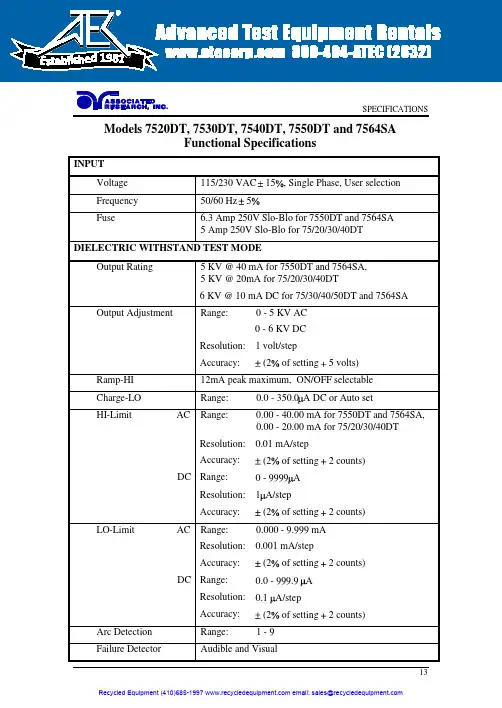
SPECIFICATIONS13Models 7520DT, 7530DT, 7540DT, 7550DT and 7564SAFunctional SpecificationsINPUTVoltage 115/230 VAC 15, Single Phase, User selection Frequency 50/60 Hz 5Fuse6.3 Amp 250V Slo-Blo for 7550DT and 7564SA 5 Amp 250V Slo-Blo for 75/20/30/40DTDIELECTRIC WITHSTAND TEST MODEOutput Rating5 KV @ 40 mA for 7550DT and 7564SA, 5 KV @ 20mA for 75/20/30/40DT6 KV @ 10 mA DC for 75/30/40/50DT and 7564SAOutput AdjustmentRange:0 - 5 KV AC 0 - 6 KV DCResolution: 1 volt/step Accuracy:(2 of setting 5 volts) Ramp-HI 12mA peak maximum, ON/OFF selectableCharge-LORange:0.0 - 350.0A DC or Auto setHI-Limit AC Range:0.00 - 40.00 mA for 7550DT and 7564SA, 0.00 - 20.00 mA for 75/20/30/40DT Resolution: 0.01 mA/step Accuracy: (2 of setting 2 counts) DC Range:0 - 9999AResolution: 1A/stepAccuracy:(2 of setting 2 counts) LO-Limit AC Range:0.000 - 9.999 mA Resolution: 0.001 mA/stepAccuracy: (2 of setting 2 counts) DC Range:0.0 - 999.9 AResolution: 0.1A/stepAccuracy:(2 of setting 2 counts) Arc Detection Range:1 - 9Failure DetectorAudible and VisualRecycledEquipment(410)email:***************************1981SPECIFICATIONS14Voltage Display Range: 0.00 - 6.00 KV Full Scale0.00 - 5.00 KV Full Scale for 7520DT onlyResolution: 10 volt/stepAccuracy: (2 of reading 2 counts)Current Display Auto RangeAC Range 1: 0.000mA - 3.500mAResolution: 0.001mA/stepRange 2: 3.00 - 40.00 mA for 7550DT and 7564SA,3.00 - 20.00 mA for 75/20/30/40DTResolution: 0.01 mA/stepDC Range 1: 0.0 A - 350.0 AResolution: 0.1A/stepRange 2: 300 A - 3500 AResolution: 1A/stepRange 3: 3000 A - 9990 AResolution: 10A/stepAccuracy: All Ranges (2 of reading 2 counts)DC Output Ripple 4**********************,ResistiveLoad Discharge Time 200 msMaximum CapacitiveLoad DC Mode1uF < 1KV0.75uF < 2KV0.5uF < 3KV0.08uF < 4KV0.04uF < 5KV0.01uF < 6KVAC Output Wave Form Sine Wave, Crest Factor = 1.3 - 1.5Output Frequency Range: 60 or 50 Hz, User SelectionAccuracy: 1%Output Regulation (1 of setting 5 volts) from no load to full load Dwell Timer Range: 0, 0.3 - 999.9 sec (0 = Constant)Resolution: 0.1 sec incrementsAccuracy: (0.1% + 0.05 sec)Ramp Timer Range: AC 0.1 - 999.9 secDC 0.4 - 999.9 secResolution: 0.1 sec incrementsAccuracy: (0.1% + 0.05 sec)RecycledEquipment(410)email:***************************SPECIFICATIONS15Ground Continuity For 75/20/30/40/50DT Current : DC 0.1 A 0.01A, fixedMax. ground resistance : 1 0.1, fixed Ground Fault Interrupt GFI Trip Current: HV Shut Down Speed: 450 A max (AC or DC)< 1msINSULATION RESISTANCE TEST MODE Model 75/30/40/50DT, 7564SAOutput VoltageRange:100 - 1000 Volts DC Resolution: 1 volt/step Accuracy:(2 of reading 2 volts) Short Circuit Current Maximum: 12mA peak Voltage DisplayRange: 0 - 1000 VResolution: 1 volt/stepAccuracy:(2 of reading 2 counts) Resistance DisplayRange: 1 - 9999 M (4 Digit, Auto Ranging)Resolution:500VDC 1000VDC M M M 0.001 1.000 - 5.388 1.000 - 9.999 0.01 1.40 - 53.88 2.80 - 99.99 0.1 14.0 - 538.8 28.0 - 999.9 1104 - 9999280 - 9999Accuracy:(2 of reading 2 counts) at test voltage 500 - 1000V and 1 - 1000 M(8 of reading 2 counts) at test voltage 500 - 1000V and 1000 - 9999 M(8 of reading 2 counts) at test voltage 100 - 500V and 0 - 1000 MCharge-LO Range: 0.000 - 3.500A or Auto Set HI-Limit Range: 0 - 9999 M (0 = Off) LO-Limit Range: 1 - 9999 MDelay TimerRange: 0, 0.5 - 999.9 sec (0 = Constant) Resolution: 0.1 sec/stepAccuracy:(0.1% + 0.05 sec)Ground Fault InterruptGFI Trip Current:HV Shut Down Speed:450 A max (AC or DC) < 1msRecycledEquipment(410)email:***************************SPECIFICATIONS16GROUND BOND TEST MODE Model 7564SA onlyOutput Voltage Range: 3.00 - 8.00 Volts AC (Open Circuit Limit) Resolution: 0.01 volt/stepAccuracy: (2 % of Setting + 0.03V ) O.C. Condition Output Frequency Range: 60 or 50 Hz, User Selection Accuracy: 1%Output CurrentRange: 3.00 - 30.00 Amps AC Resolution: 0.01 Amp/stepAccuracy :(2 % of Setting + 0.02 A) Current DisplayRange: 0.00 - 30.00 Amps Resolution: 0.01 Amp/stepAccuracy:(3 % of Reading + 0.03 A) Resistance DisplayRange: 0 - 600 m Resolution: 1 m /stepAccuracy:(2 % of Reading + 2 m ) HI-LimitRange: 0 - 600 m for 3 - 10 A 0 - 150 m for 3 - 30 A Resolution: 1 m /stepAccuracy:(2 % of Setting + 2 m ) LO-LimitRange: 0 - 600 m for 3 - 10 A 0 - 150 m for 3 - 30 A Resolution: 1 m /stepAccuracy:(2 % of Setting + 2 m ) Dwell TimerRange: 0, 0.5 - 999.9 sec (0 = Constant) Resolution: 0.1 sec/step Accuracy:(0.1% + 0.05 sec)Milliohm OffsetMax. Offset Capability: 200 mResolution: 1 m / stepAccuracy:(2 % of Setting + 2 m )RecycledEquipment(410)email:***************************SPECIFICATIONS17GENERAL SPECIFICATIONSPLC Remote Control Input - Test, Reset, Recall memory 1, 2 and 3Output - Pass, Fail, Test-in-ProcessMemory Allows storage of up to 50 groups different test programsand 8 step/each memory. Step is not available on 7520DT SecurityProgrammable password lockout capability to avoid unauthorized access to test set-up program. LCD Contrast Setting 9 ranges set by the numeric keys on the front panel. Buzzer Volume Setting 10 ranges set by the numeric key on the front panel.Calibration Software and adjustments are made through front panel. Mechanical Bench or rack mount with tilt up front feet. Dimension7540DT, 7550DT and 7564SA:(W x H x D) 17 x 5.8 x 20.3 in. (432 x 147 x 515 mm) 7520DT and 7530DT:(W x H x D) 17 x 5.8 x 12 in. (432 x 147 x 305 mm)Weight7564SA without scanner 52.5 lbs (24 Kgs) 7564SA with built-in scanner 57.0 lbs (26 Kgs) 7550DT without scanner 50.5 lbs (23 Kgs) 7550DT with built-in scanner 55.0 lbs(25 Kgs) 7540DT with 4 port scanner 39.6 lbs (18 Kgs) 7540DT with 8 port scanner41.8 lbs(19 Kgs) 7530DT scanner not available 24.8 lbs (11.27 Kgs) 7520DT scanner not available 24.8 lbs(11.27 Kgs)Scanner Port Two Port Maximum including the built-in scanner. Not available on 7520DT, 7530DT and 7540DT.Scanner Built-in OptionHigh Voltage x 4 Ports (7540DT only)High Voltage x 8 Ports (75/40/50DT and 7564SA) Ground Bond x 8 Ports (7564SA only)RecycledEquipment(410)email:***************************。

目录前言 (1)产品概述 (2)产品性能 (2)部件介绍 (3)安装说明 (4)显示面板说明 (5)参数设置 (5)操作简图 (9)物件探测调节 (10)装箱清单 (10)技术参数 (11)注意事项 (12)常见故障及解决办法 (12)干扰说明 (13)前言首先,感谢你购买本公司的金属探测门!!!本说明书对本产品进行了充分的描述与说明,在使用本产品前,您可以花一小段时间来阅读本说明书,这样您可以更了解本产品的性能,更好的去操作,同时您也能看到本产品更好的性能。
金属探测门可以应用于机场,监狱,考场,工厂等场所,对通过的人体进行准确检测身上是否携带金属物品。
本说明书对通过式金属探测门的安装与使用进行了详细的说明。
适用对象为使用产品客户,了解产品潜在客户等群体。
注意:本公司有权对本说明书及产品进行变更,如有变更,恕不另行通知。
本说明书编制过程中力求内容的准确和完善,但不保证本说明书没有任何错误或漏失,若有错误与缺失之处,欢迎来电赐教,我们将把您的意见作为修正参考意见之一。
- 1 -- 2 -我公司生产的802标准版通过式金属探测门采用了国际先进技术,专门用于对人身上隐藏的金属及合金物品的探测防范,它安全性高,适用性强,灵敏度高,探测范围广,抗外界干扰能力强,能够全天智能工作,并可以声光同时报警,在质量,效果,技术上均达到了世界领先水平,它可以调节灵敏度,最高精确探测可以小到曲形别针大小的金属物,并可以区分人体隐藏的具体位置,用户还可以根据金属的大小,体积,重量等进行灵敏度的设置,以排除钥匙,首饰,皮带金属扣而产生的误报警,而且本产品还可以防止贵重物品的流失,如海关,生产重金属工厂,私人毫宅等地方,都可以购买本产品作为一道安全防护。
因此安装本公司生产的通过式金属探测门是你英明的选择!◆ 六个探测区域:6个相互重叠的探测区域划分,准确判断金属物品的位置。
◆ 报警区域指示:在门的两边或主机箱有与人体等高的报警部位指示灯,配和声音,一目了然,大大提高工作效率。
1DS8025-02 March 2011Features2.5V to 5.5V Input RangeAdjustable Output From 0.5V to V IN1.0V, 1.2V, 1.3V, 1.5V, 1.8V,2.5V and3.3V Fixed/Adjustable Output Voltage 400mA Output Current 95% EfficiencyNo Schottky Diode Required1.25MHz Fixed Frequency PWM Operation Small SOT-23-5 and TSOT-23-5 PackageRoHS Compliant and Halogen FreeApplicationsCellular T elephonesPersonal Information Appliances Wireless and DSL Modems MP3 PlayersPortable Instruments1.25MHz, 400mA, High Efficiency PWM Step-Down DC/DC ConverterGeneral DescriptionThe RT8025 is a high-efficiency pulse-width-modulated (PWM) step-down DC/DC converter. Capable of delivering 400mA output current over a wide input voltage range from 2.5 to 5.5V, the RT8025 is ideally suited for portable electronic devices that are powered from 1-cell Li-ion battery or from other power sources within the range such as cellular phones, PDAs and handy-terminals.Internal synchronous rectifier with low R DS(ON) dramatically reduces conduction loss at PWM mode. No external Schottky diode is required in practical application. The RT8025 automatically turns off the synchronous rectifier while the inductor current is low and enters discontinuous PWM mode. This can increase efficiency at light load condition.The RT8025 enters Low-Dropout mode when normal PWM cannot provide regulated output voltage by continuously turning on the upper P-MOSFET . RT8025 enter shutdown mode and consumes less than 0.1μA when EN pin is pulled low.The switching ripple is easily smoothed-out by small package filtering elements due to a fixed operation frequency of 1.25MHz. This along with small SOT-23-5and TSOT-23-5 package provides small PCB area application. Other features include soft start, lower internal reference voltage with 2% accuracy, over temperature protection, and over current protection.Ordering InformationPin Configurations(TOP VIEW)SOT-23-5/TSOT-23-5VIN GND ENNote :Richtek products are :` RoHS compliant and compatible with the current require-ments of IPC/JEDEC J-STD-020.` Suitable for use in SnPb or Pb-free soldering processes.Default : Adjustable 10 : 1.0V 12 : 1.2V 13 : 1.3V 15 : 1.5V 18 : 1.8V 25 : 2.5V 33 : 3.3VMarking InformationFor marking information, contact our sales representative directly or through a Richtek distributor located in your area.2DS8025-02 March 2011 Typical Application Circuit0.5VV and 1M R2R1 with R2R11 x V V REF(Typ.)REF OUT =Ω≤+⎟⎠⎞⎜⎝⎛+=Layout GuideLayout note:1.The distance that C IN connects to V IN is as close as possible (Under 2mm).2. C OUT should be placed near RT8025.Figure 3V OUTV INV OUT3DS8025-02 March 2011Function Block DiagramLXFB/VOUTGND4DS8025-02 March 2011Absolute Maximum Ratings (Note 1)Supply Input Voltage ------------------------------------------------------------------------------------------------------6.5VEnable, FB Voltage -------------------------------------------------------------------------------------------------------V IN + 0.6VPower Dissipation, P D @ T A = 25°CSOT-23-5, TSOT-23-5-----------------------------------------------------------------------------------------------------0.4WPackage Thermal Resistance (Note 2)SOT-23-5, TSOT-23-5, θJA -----------------------------------------------------------------------------------------------250°C/W SOT-23-5, TSOT-23-5, θJC -----------------------------------------------------------------------------------------------130°C/W Junction T emperature Range --------------------------------------------------------------------------------------------150°C Lead Temperature (Soldering, 10 sec.)-------------------------------------------------------------------------------260°CStorage T emperature Range --------------------------------------------------------------------------------------------−65°C to 150°CESD Susceptibility (Note 3)HBM (Human Body Mode)----------------------------------------------------------------------------------------------2kV MM (Machine Mode)------------------------------------------------------------------------------------------------------200VElectrical CharacteristicsRecommended Operating Conditions (Note 4)Supply Input Voltage ------------------------------------------------------------------------------------------------------2.5V to 5.5V Junction T emperature Range --------------------------------------------------------------------------------------------−40°C to 125°CAmbient T emperature Range --------------------------------------------------------------------------------------------−40°C to 85°C5DS8025-02 March 2011Note 1. Stresses listed as the above “Absolute Maximum Ratings ” may cause permanent damage to the device. These are forstress ratings. Functional operation of the device at these or any other conditions beyond those indicated in the operational sections of the specifications is not implied. Exposure to absolute maximum rating conditions for extended periods may remain possibility to affect device reliability.Note 2. θJA is measured in the natural convection at T A = 25°C on a low effective thermal conductivity test board ofJEDEC 51-3 thermal measurement standard.Note 3. Devices are ESD sensitive. Handling precaution recommended.Note 4. The device is not guaranteed to function outside its operating conditions.Note 5. ΔV = I OUT x R DS(ON)_P6DS8025-02 March 2011 Typical Operating CharacteristicsFrequency vs. Temperature1.101.121.141.161.181.201.221.241.26-50-25255075100125Temperature F r e q u e n c y (M H z )(°C)Frequency vs. Input Voltage2.5 2.83.1 3.4 3.744.3 4.6 4.95.2 5.5Input Voltage (V)F r e q u e n c y (M H z )Current Limit vs. Input Voltage2.5 2.83.1 3.4 3.744.3 4.6 4.95.2 5.5Input Voltage (V)C u r r e n t L i m i t (A )Reference vs. Input Voltage2.52.83.13.43.744.34.64.95.25.5Input Voltage (V)R e f e r e n c e (V )Efficiency vs. Load Current1020304050607080901000.010.110.210.310.410.510.61Load Current (A)E f f i c i e n c y (%)Load Regulation0.10.150.20.250.30.350.4Load Current (A)7DS8025-02 March 2011Reference vs. Temperature0.4900.4930.4950.4980.5000.5030.5050.5080.510-50-25255075100125Temperature R e f e r e n c e (V )(°C)Load Transient ResponseTime (50μs/Div)I OUT(200mA/Div)V OUT (20mV/Div)V IN = 3.3V, V OUT = 1.8V, I OUT = 100mA to 400mALoad Transient Response Time (50μs/Div)I OUT(200mA/Div)V OUT (20mV/Div)V IN = 3.3V, V OUT = 1.8V, I OUT = 200mA to 400mAOutput RippleTime (500ns/Div)V OUT (5mV/Div)V LX (5V/Div)I LX(500mA/Div)V IN = 3.3V, V OUT = 1.8V, I OUT = 400mAPower OnTime (100μs/Div)V EN (5V/Div)V OUT (1V/Div)I IN(200mA/Div)V IN = 3.3V, V OUT = 1.8V, I OUT = 400mAPower OffTime (100μs/Div)V EN (5V/Div)V OUT (2V/Div)I IN(200mA/Div)V IN = 3.3V, V OUT = 1.8V, I OUT = 400mA8DS8025-02 March 2011 ⎦⎤⎢⎣⎡+≤OUT L OUT 8fC 1ESR ΔI ΔV Applications InformationThe basic RT8025 application circuit is shown in Typical Application Circuit. External component selection is determined by the maximum load current and begins with the selection of the inductor value and operating frequency followed by C IN and C OUT .Inductor SelectionFor a given input and output voltage, the inductor value and operating frequency determine the ripple current. The ripple current ΔI L increases with higher V IN and decreases with higher inductance.Having a lower ripple current reduces the ESR losses inthe output capacitors and the output voltage ripple. Highest efficiency operation is achieved at low frequency with small ripple current. This, however, requires a large inductor.A reasonable starting point for selecting the ripple current is ΔI L = 0.4(I MAX ). The largest ripple current occurs at the highest V IN . To guarantee that the ripple current stays below a specified maximum, the inductor value should be chosen according to the following equation :Inductor Core SelectionOnce the value for L is known, the type of inductor must be selected. High efficiency converters generally cannot afford the core loss found in low cost powdered iron cores,forcing the use of more expensive ferrite or mollypermalloy cores. Actual core loss is independent of core size for a fixed inductor value but it is very dependent on the inductance selected. As the inductance increases, core losses decrease. Unfortunately, increased inductance requires more turns of wire and therefore copper losses will increase.Ferrite designs have very low core losses and are preferred at high switching frequencies, so design goals can concentrate on copper loss and preventing saturation.Ferrite core material saturates “hard ”, which means that inductance collapses abruptly when the peak design current is exceeded. This results in an abrupt increase in⎦⎤⎢⎣⎡−⎥⎦⎤⎢⎣⎡×=IN OUT OUT L V V 1L f V ΔI ⎥⎥⎦⎤⎢⎢⎣⎡−⎥⎦⎤⎢⎣⎡Δ×=IN(MAX)OUT L(MAX)OUT V V 1I f V L inductor ripple current and consequent output voltage ripple.Do not allow the core to saturate!Different core materials and shapes will change the size/current and price/current relationship of an inductor.T oroid or shielded pot cores in ferrite or permalloy materials are small and don ’t radiate energy but generally cost more than powdered iron core inductors with similar characteristics. The choice of which style inductor to use mainly depends on the price vs size requirements and any radiated field/EMI requirements.C IN and C OUT SelectionThe input capacitance, C IN , is needed to filter the trapezoidal current at the source of the top MOSFET. To prevent large ripple voltage, a low ESR input capacitor sized for the maximum RMS current should be used. RMS current is given by :1V V V V I I OUTININOUT OUT(MAX)RMS −=This formula has a maximum at V IN = 2V OUT , where I RMS = I OUT /2. This simple worst-case condition is commonly used for design because even significant deviations do not offer much relief. Note that ripple current ratings from capacitor manufacturers are often based on only 2000hours of life which makes it advisable to further derate the capacitor, or choose a capacitor rated at a higher temperature than required. Several capacitors may also be paralleled to meet size or height requirements in the design.The selection of C OUT is determined by the effective series resistance (ESR) that is required to minimize voltage ripple and load step transients, as well as the amount of bulk capacitance that is necessary to ensure that the control loop is stable. Loop stability can be checked by viewing the load transient response as described in a later section.The output ripple, ΔV OUT , is determined by :The output ripple is highest at maximum input voltagesince ΔI L increases with input voltage. Multiple capacitors placed in parallel may be needed to meet the ESR and RMS current handling requirements. Dry tantalum, special9DS8025-02 March 2011Output Voltage ProgrammingThe resistive divider allows the V FB pin to sense a fraction of the output voltage as shown in Figure 4.R2R1(1V V REF OUT +=where V REF is the internal reference voltage (0.5V typ.)Efficiency ConsiderationsThe efficiency of a switching regulator is equal to the output power divided by the input power times 100%. It is often useful to analyze individual losses to determine what is limiting the efficiency and which change would produce the most improvement. Efficiency can be expressed as :Efficiency = 100% − (L1+ L2+ L3+ ...)where L1, L2, etc. are the individual losses as a percentage of input power. Although all dissipative elements in the circuit produce losses, two main sources usually account for most of the losses : VIN quiescent current and I 2R losses. The VIN quiescent current loss dominates the efficiency loss at very low load currents whereas the I 2R loss dominates the efficiency loss at medium to high load currents. In a typical efficiency plot, the efficiency curve at very low load currents can be misleading since the actual power lost is of no consequence.1. The VIN quiescent current is due to two components :the DC bias current as given in the electrical characteristics and the internal main switch and synchronous switch gate charge currents. The gate charge current results from switching the gate capacitance of the internal power MOSFET switches. Each time the gate is switched from high to low to high again, a packet of charge ΔQ moves from V IN to ground.The resulting ΔQ/Δt is the current out of V IN that is typically larger than the DC bias current. In continuous mode,I GATECHG = f(Q T +Q B )where Q T and Q B are the gate charges of the internal top and bottom switches. Both the DC bias and gate charge losses are proportional to V IN and thus their effects will be more pronounced at higher supply voltages.2. I 2R losses are calculated from the resistances of the internal switches, R SW and external inductor R L . In continuous mode the average output current flowing through inductor L is “chopped ” between the main switch and the synchronous switch. Thus, the series resistance looking into the LX pin is a function of both top and bottom MOSFET R DS(ON) and the duty cycle (DC) as follows :R SW = R DS(ON)TOP x DC + R DS(ON)BOT x (1−DC)The R DS(ON) for both the top and bottom MOSFETs can be obtained from the Typical Performance CharacteristicsFor adjustable about voltage mode, the output voltage is set by an external resistive divider according to the following equation :polymer, aluminum electrolytic and ceramic capacitors are all available in surface mount packages. Special polymer capacitors offer very low ESR but have lower capacitance density than other types. Tantalum capacitors have the highest capacitance density but it is important to only use types that have been surge tested for use in switching power supplies. Aluminum electrolytic capacitors have significantly higher ESR but can be used in cost-sensitive applications provided that consideration is given to ripple current ratings and long term reliability. Ceramic capacitors have excellent low ESR characteristics but can have a high voltage coefficient and audible piezoelectric effects.The high Q of ceramic capacitors with trace inductance can also lead to significant ringing.Using Ceramic Input and Output CapacitorsHigher values, lower cost ceramic capacitors are now becoming available in smaller case sizes. Their high ripple current, high voltage rating and low ESR make them ideal for switching regulator applications. However, care must be taken when these capacitors are used at the input and output. When a ceramic capacitor is used at the input and the power is supplied by a wall adapter through long wires, a load step at the output can induce ringing at the input, V IN . At best, this ringing can couple to the output and be mistaken as loop instability. At worst, a sudden inrush of current through the long wires can potentially cause a voltage spike at V IN large enough to damage the part.Figure 4. Setting the Output VoltageV OUT10DS8025-02 March 2011 Checking Transient ResponseThe regulator loop response can be checked by looking at the load transient response. Switching regulators take several cycles to respond to a step in load current. When a load step occurs, V OUT immediately shifts by an amount equal to ΔI LOAD (ESR), where ESR is the effective series resistance of C OUT . ΔI LOAD also begins to charge or discharge C OUT generating a feedback error signal used by the regulator to return V OUT to its steady-state value.During this recovery time, V OUT can be monitored for overshoot or ringing that would indicate a stability yout ConsiderationsFollow the PCB layout guidelines for optimal performance of RT8025.` For the main current paths as indicated in bold lines inFigure 6 keep their traces short and wide.` Put the input capacitor as close as possible to the devicepins (VIN and GND).` LX node is with high frequency voltage swing and shouldbe kept small area. Keep analog components away from LX node to prevent stray capacitive noise pick-up.curves. Thus, to obtain I 2R losses, simply add R SW to R L and multiply the result by the square of the average output current.Other losses including C IN and C OUT ESR dissipative losses and inductor core losses generally account for less than 2% of the total loss.Thermal ConsiderationsThe maximum power dissipation depends on the thermal resistance of IC package, PCB layout, the rate of surroundings airflow and temperature difference between junction to ambient. The maximum power dissipation can be calculated by following formula :P D(MAX) = ( T J(MAX) - T A ) / θJAWhere T J(MAX) is the maximum operation junction temperature 125°C, T A is the ambient temperature and the θJA is the junction to ambient thermal resistance.For recommended operating conditions specification of RT8025 DC/DC converter, where T J (MAX) is the maximum junction temperature of the die (125°C) and T A is the maximum ambient temperature. The junction to ambient thermal resistance θJA is layout dependent. For SOT-23-5/TSOT-23-5 packages, the thermal resistance θJA is 250°C/W on the standard JEDEC 51-3 single-layer thermal test board. The maximum power dissipation at T A = 25°C can be calculated by following formula :P D(MAX) = ( 125°C - 25°C ) / 250 = 0.4 W for SOT-23-5/TSOT-23-5 packagesThe maximum power dissipation depends on operating ambient temperature for fixed T J(MAX) and thermal resistance θJA . For RT8025 packages, the Figure 5 of derating curves allows the designer to see the effect of rising ambient temperature on the maximum power allowed.The value of junction to case thermal resistance θJC is popular for users. This thermal parameter is convenient for users to estimate the internal junction operated temperature of packages while IC operating. It's independent of PCB layout, the surroundings airflow effects and temperature difference between junction to ambient.The operated junction temperature can be calculated by following formula :T J = T C + P D x θJCWhere T C is the package case (Pin 2 of package leads)temperature measured by thermal sensor, P D is the power dissipation defined by user's function and the θJC is the junction to case thermal resistance provided by IC manufacturer. Therefore it's easy to estimate the junction temperature by any condition.Figure 5. Derating Curves for RT8025 Package 05010015020025030035040045020406080100120140Ambient Temperature (°C)M a x i m u m P o w e r D i s s i p a t i o n (m W )RT802511DS8025-02 March 2011Table 2. Capacitors for C IN and C OUTRecommended component selection for Typical Application` Connect feedback network behind the output capacitors.Keep the loop area small. Place the feedback components near the RT8025.` Connect all analog grounds to a command node andthen connect the command node to the power ground behind the output capacitors.C410uFFigure 6. EVB SchematicRT802512DS8025-02 March 2011Outline DimensionA1HLSOT-23-5 Surface Mount PackageRT802513DS8025-02 March 2011Richtek Technology CorporationHeadquarter5F, No. 20, Taiyuen Street, Chupei City Hsinchu, Taiwan, R.O.C.Tel: (8863)5526789 Fax: (8863)5526611Information that is provided by Richtek Technology Corporation is believed to be accurate and reliable. Richtek reserves the right to make any change in circuit design, specification or other related things if necessary without notice at any time. No third party intellectual property infringement of the applications should be guaranteed by users when integrating Richtek products into any application. No legal responsibility for any said applications is assumed by Richtek.Richtek Technology CorporationTaipei Office (Marketing)5F, No. 95, Minchiuan Road, Hsintien City Taipei County, Taiwan, R.O.C.Tel: (8862)86672399 Fax: (8862)86672377Email:*********************TSOT-23-5 Surface Mount PackageA1HL。
DatasheetHP OfficeJet Pro8025All-in-OnePrinterThe productive smart printer that doesn't just print,it produces.Help save time with Smart Tasks shortcuts,1and get automatic two-sided printing.Print and scan from your phone,1Save up to50% on ink with HP Instant Ink.3Dynamic security enabled printer.Intended to be used with cartridges using only HP original electronic circuitry. Cartridges with modified or non-HP electronic circuitry may not work,and those that work today may not work in the future./go/learnaboutsuppliesISO Speed:Black:Up to20ppm;Color:Up to10ppmPrint Resolution:Black(best):Up to1200x1200rendered dpi;Color(best):Up to4800x1200optimized dpi on HP Advance Photo Paper1200x1200dpi inputScan Resolution:Hardware:Up to1200x1200dpi;Optical: Up to1200dpiCopy Resolution:Black(text&graphics):Up to600dpi;Color (text&graphics):Up to600dpiFax Resolution:Black(best):Up to Up to300x300dpi;Color (best):200x200dpiStandard Connectivity:1Ethernet;1Wireless802.11b/g/n;1 RJ-11FaxMobile Printing Capability:HP Smart;Apple AirPrint™;Wi-Fi®Direct Printing;Mopria™CertifiedDuty cycle:Monthly(letter):Up to20,000pages Display:2.7"(6.86cm)Capacitive TouchscreenCGDDesigned to save you time●Eliminate steps in repetitive tasks,using Smart Tasks.1Scan to the cloud,email,and more–in a tap.1●Work fast and hands-free with the35-page auto-feeder.Get automatic two-sided printing.●Take control of print,scan,copy,and fax jobs with tap-and-swipe ease,using the color touchscreen.●This printer is made from recycled plastics and other electronics—up to15%by weight of plastic.●HP Voice-activated printing enables your HP printer to work with Amazon Alexa and Google Assistant™.7Freedom to work anywhere●Connect to cloud-based printing with Wi-Fi or your cellular network to print from anywhere.1●Quickly access and print documents and images on your smartphone,from Dropbox and Google Drive.1●Get high-quality scanning to share to Dropbox,Google Drive,email,or the cloud–from virtually anywhere.1●Take a photo as a copy, and send it to your printer from virtually anywhere.1●Get notifications when printing,scanning,or copying from your smartphone.1Save up to50%on ink●Save on ink and get it automatically delivered right on time.3,6●Create vibrant,professional-quality color graphics,ideal for office use and presentations.●Get rich black text for all your business documents.Enhanced security, reliable connections●Reduce interruptions with self-healing Wi-Fi that keeps you connected.3●Get best-in-class security to help protect devices, data, and documents.5●Get security essentials to help maintain privacy and control.●Count on chatbot support and helpful notifications with the HP Smart app.1●Easily share resources – access and print with wireless and Ethernet networking.31Requires the HP Smart app download.For details on local printing requirements see /go/mobileprinting.2Wireless operations are compatible with2.4GHz and5.0GHz operations only.Learn more at /go/mobileprinting.Wi-Fi is a registered trademark of Wi-Fi Alliance®.3FOR U.S.:Based on monthly subscription cost using only all pages in plan vs.cost per page of most color inkjet cartridge printers<$399.Share of New Inkjet Unit Shipments(<$399)for2018Q1period in the US from IDC 2018Q1Final Release.Standard cartridge CPP from gap intelligence7/24/18.FOR CAN:Based on monthly subscription cost using only all pages in plan vs.cost per page of most color inkjet cartridge printers<$399CAD.Standard cartridge CPP from internal research.Share of New Inkjet Unit Shipments(<$399)for2018Q1period in Canada from IDC2018Q1Final Release.4For more details,see /HPOfficeJetPro.5Compared to the majority of competing in-class consumer color desktop inkjet all-in-ones <$299 USD. Keypoint Intelligence - Buyers Lab 2018 research study commissioned by HP based on research survey of printer manufacturers’ published specifications, sustainability reports, and press releases as of 12/15/2018 and not confirmed by lab testing. Market share as reported by IDC CYQ3 2018 Hardcopy Peripherals Tracker, 2018Q3 Release. AiO with best in-class security features based on review of published embedded security features of competitive in-class models and defined as offering business-class, multi-point security, including but not limited to: encryption at the level of data, device, network, document; enterprise-class Wi-Fi security; and secure printing. For more details, see HPOfficeJetPro.6Based on plan usage,Internet connection to eligible HP printer,valid credit/debit card,email address,and delivery service in your geographic area.7 Requires Amazon Alexa or Google Assistant™ and is available in certain countries; see /go/alexa and/go/hpgooglehome. Also requires an HP web-connected printer registered with Google Cloud Print or ePrint. For ePrint account registration, /go/HPConnected/help/eprint.Datasheet |HP OfficeJet Pro 8025All-in-One PrinterHP OfficeJet Pro 8025All-in-One Printer Specifications TableFunctions / Multitasking supported Print,copy,scan,fax /YesPrint Speed 5 6Letter:Up to 20ppm;Black (ISO):Up to 20ppm;Color (ISO):Up to 10ppm;First Page Out Black :As fast as 13sec ;First Page Out Color :As fast as 17sec ;Black (Draft):Up to 29ppm;Color (Draft):Up to 25ppmPrint Resolution Black (best):1200x 1200rendered dpi;Color (best):Up to 4800x 1200optimized dpi on HP Advance Photo Paper 1200x 1200dpi input Print Technology HP Thermal Inkjet Printer Drivers Included HP PCL3GUIPrint Cartridges Number 4(1each black,cyan,magenta,yellow)Borderless Printing Yes (up to 8.5x 11in,216x 279mm)Standard Print languages HP PCL3GUIPrinter Smart Software FeaturesOrientation: Portrait/Landscape; Print on Both Sides: None/Flip on Long Edge/Flip on Short Edge;Page Order:Front to Back/Back to Front;Pages per Sheet:1,2,4,6,9,16;Quality Settings:Draft/Normal/Best;Printing Shortcuts;Print in Grayscale:Off/High Quality Grayscale/Black Ink Only;Pages per Sheet Layout:Right then Down/Down then Right/Left then Down/Down then Left;Print in Max DPI:No/Yes;HP Real Life Technologies:Off/On;Booklet:None/Booklet-Left Binding/Booklet-Right Binding;Pages to Print:Print All Pages/Print Odd Pages Only/Print Even Pages Only;Borderless Printing:Off/On;Page Borders:Off/On Printer Management Embedded Web ServerScan Type / Technology Flatbed,ADF /Contact Image Sensor (CIS)Scan Resolution Hardware :Up to 1200x 1200dpi;Optical :Up to 1200dpi Scan File Format JPG,BMP ,TIFF ,PDF ,RTF ,TXT ,PNGScan Input Modes Front-panel scan,copy,fax,HP Software,EWSScan Size ADF :8.5x 14in (one-sided),A4,Letter (one-sided)Maximum;5x 5in Minimum Flatbed :8.5x 11.7inScan SpeedUp to 8ppm (200ppi,b&w),Up to 3.5ppm (200ppi,color)Scanner Advanced FeaturesOCR (Optical Character Recognition); Smart Taks shortcuts: 1-click customizable scan to cloud destinations, email, and print, create editable, searchable documents by scanning from phone or printer; Smart Tasks destinations: Dropbox, Google Drive, One drive, email recipients, print Bit depth / Grayscale levels 24-bit /256Digital Sending Standard Features Scan to PCCopy Speed Black (ISO):Up to 13cpm;Color (ISO):Up to 7cpm;Black (Draft):Up to 29cpm;Color (Draft):Up to 23cpmCopy ResolutionBlack (text and graphics):Up to 600dpi;Up to 600dpi;Color (text and graphics):Up to 600dpi Maximum Number Of Copies Up to 99copies Copier Resize 25to 400%Copier Settings Number of Copies;Resize;Quality;Lighter/Darker;Paper size;Paper Type;Two-sided;ID Copy,Collate;Margin shift;Enhancement;Crop;Copy preview Fax Speed Up to :4sec per page;Letter :4sec per pageFax ResolutionBlack (best):Up to 300x 300dpi;Color (best):200x 200dpi;Black (standard):203x 98dpi;Color (standard):200x 200dpiFax Smart Software Features Digital Fax -Fax to PC is available with Windows (Please use:Visit /support to download the latest software.Fax FeaturesFax Memory :Up to 100pages;Auto Fax Reduction Supported :Yes;Auto-Redialing :Yes;Fax Delayed Sending :Yes;Distinctive Ring Detection Supported :Yes;Fax Forwarding Supported :Yes;Fax Phone TAM Interface Supported :No;Fax Polling Supported :No;Fax Telephone Mode Supported :No;Junk Barrier Supported :Yes,requires Caller ID;Maximum Speed Dialing Numbers :Up to 99numbers;PC Interface Supported :Yes,PC fax send and archive;Remote Retrieval Capability Supported :No;Telephone Handset Supported :NoStandard Connectivity 1Ethernet;1Wireless 802.11b/g/n;1RJ-11Fax Network Capabilities Yes,via built-in Ethernet;Wireless 802.11b/g/n Wireless Capability Yes,built-in WiFi 802.11b/g/nMobile Printing Capability 4Apple AirPrint™;Wi-Fi®Direct Printing;Mopria™Certified;HP Smart Memory Standard :256MB;Maximum :256MB DDR3SDRAM Processor Speed 1200MHzDuty Cycle 7Monthly,letter :Up to 20,000pages Recommended Monthly Page VolumeUp to 800pagesMedia Types SupportedPlain Paper ,HP Photo Papers,HP Matte Brochure or Professional Paper ,HP Matte Presentation Paper ,HP Glossy Brochure or Professional Paper ,Other Photo Inkjet Papers,Other Matte Inkjet Papers,Other Glossy Inkjet Papers,Thick Plain Paper ,Light/Recycled Plain Paper ,HP Tri-fold Brochure Paper ,Glossy Media Weight SupportedPlain paper:16to 28lb,BondMedia Sizes SupportedA4;A5;A6;B5(JIS);6x 8in;Executive;Index card 3.5x 5in;Index card 4x 6in;Index card 5x 8in;Index card A4;Index card Letter;3.5x 5in;4x 6in;5x 7in;13x 18cm;8x 10in;10x 15cm;L;Photo 2L;8.5x 13in;Letter;Statement;Envelope #10;Envelope C5;Envelope C6;Envelope DL;Envelope Monarch;Card Envelope 4.4x 6in Media Sizes Custom Tray 1:3x 5to 8.5x 14inPaper Handling225-sheet input tray,35-sheet ADF;60-sheet output tray;Duplex Options :Automatic (standard);Auto Document Feeder Capacity :Standard,35sheets;Envelope Feeder :No;Standard Paper Trays :1;Input Capacities :Up to 225sheets standard;Up to 10envelopes;Up to 225sheets legal;Output Capacities :Up to 60sheets standard;Up to 10envelopes labels;Up to 60sheets legalWhat's in the box1KR57A HP OfficeJet Pro 8025 All-in-One Printer; HP 910 Setup Black Instant Ink Ready Cartridge; HP 910 Setup Cyan Instant Ink Ready Cartridge; HP 910 Setup Magenta Instant Ink Ready Cartridge; HP 910 Setup Yellow Instant Ink ReadyCartridge; Ink Caution Flyer; Power Cord; Setup Poster; Reference Guide; Instant Ink Flyer.Replacement CartridgesHP 910Black Original Ink Cartridge (~300pages)3YL61AN;HP 910Cyan Original Ink Cartridge 3YL58AN;HP 910Magenta Original Ink Cartridge 3YL59AN;HP 910Yellow Original Ink Cartridge 3YL60AN (CMY composite ~315pages);HP 910XL Black Original Ink Cartridge (~825pages)3YL65AN;HP 910XL Cyan Original Ink Cartridge 3YL62A;HP 910XL Magenta Original Ink Cartridge 3YL63A;HP 910XL Yellow Original Ink Cartridge 3YL64AN (CMY composite pages ~825);HP 916XL Black Original InkCartridge 3YL66AN (~1,500pages).Actual yield varies considerably based on content of printed pages and other factors.For details see /go/learnaboutsuppliesInstant ink eligible HP Instant Ink eligible /Save up to 50%on ink.For more information visit Product Dimensions 1W x D x H :18.11x 13.43x 9.21in;Maximum :18.11x 20.13x 9.17in Product Weight 218.04IbWarranty FeaturesOne-year limited hardware warranty;For more info please visit us at Control Panel 2.7"(6.86cm)Capacitive Touchscreen CGD (color graphics)Display Description 2.7"(6.86cm)Capacitive Touchscreen CGD Software IncludedHP Printer Software,Shop for Supplies OnlineCompatible Operating SystemsWindows 10,8.1,8,7,Windows Server 2008R264-bit,Windows Server 2008R264-bit (SP1),Windows Server 201264-bit,Windows Server 2012R264-bit,Windows Server 2016Compatible Network Operating SystemsWindows 10,8.1,8,7:32-bit or 64-bit,2GB available hard disk space,CD-ROM/DVD drive or Internet connection,USB port,Internet Explorer ,USB port,Internet Explorer 8;any Intel Pentium II,Celeron or 233MHz compatible processor ,850MB available hard disk space,CD-ROM/DVD drive or Internet connection,USB port,Internet Explorer 8;Linux (For more information,see /hplip-web/index.html)Minimum System RequirementsPC : Windows 10, 8.1, 8, 7: 1 GHz 32-bit (x86) or 64-bit (x64) processor , 2 GB available hard disk space,CD-ROM/DVD drive or Internet connection,USB port,InternetExplorer;MAC :OS X v10.11El Capitan;macOS Sierra v10.12(previously OS X);macOS High Sierra v10.13;1.5GB available space;Internet accessPower 3Power Supply Type :Internal;Power Requirements :Input voltage:100to 240VAC (+/-10%),50/60Hz (+/-3Hz)AcousticsAcoustic Power Emissions :6.8B(A)(printing at 16ppm);Acoustic Pressure Emissions :62dB(A)(Draft printing at 17ppm)Operating EnvironmentOperating Temperature Range :41to 104°F;Recommended Operating Temperature :59to 86°F;Storage Temperature Range :-40to 140°F;Operating Humidity Range :20to 80%RH;Recommended Humidity Operating Range :20to 75%RH AccessoriesNoneLearn more at 1Dimensions vary as per configuration 2Weight varies as per configuration 3Power requirements are based on the country/region where the printer is sold.Do not convert operating voltages.This will damage the printer and void the product warranty.4Wireless performance is dependent upon physical environment and distance from the access point.Wireless operations are compatible with 2.4GHz routers only;excludes wireless direct.Wireless direct may require driver or apps be installed and connected on wireless-enabled mobile device or PC.Wireless functionality may vary by computer and mobile operating systems,see .Separately purchased data plans or usage fees may apply.Print times and connection speeds may vary.AirPrint supports OS X v10.11El Capitan and devices running iOS 4.2or later and requires the printer be connected to the same network as your OS X or iOS device.AirPrint,the AirPrint Logo,iPad,iPhone,and iPod touch are trademarks of Apple®Inc.Windows is a trademark of the Microsoft group of companies.5Speed specifications have been updated to reflect current industry testing methods.6]Either after first page or after first set of ISO test pages.For details see /go/printerclaims 7HP recommends that the number of printed pages per month be within the stated range for optimum device performance,based on factors including supplies replacement 8For more information about page yields for replacement cartridges see /go/learnaboutsupplies for setup cartridges click on Setup supplies link on the same page.© Copyright 2019 HP Development Company, L.P. The information contained herein is subject to change without notice. The only warranties for HP products and services are set forth in the express warranty statements accompanying such products and services. Nothing herein should be construed as constituting an additional warranty. HP shall not be liable for technical or editorial errors or omissions contained herein. ENERGY STAR and the ENERGY STAR logo are registered U.S. marks. Windowsis a registered trademark of Microsoft Corporation. AirPrint, iPad, iPhone, and iPod touch are trademarks of Apple Inc., registered in the U.S. and other countries.January 2019Energy Efficiency Compliance ENERGY STAR®qualified。
出租车计价器内部时钟稳定性实验及分析徐俊杰【摘要】提出了一种利用北斗定位系统所提供的高精度UTC作为参考时钟源,检测出租车计价器(以下称计价器)内部时钟稳定性及环境温度适应性的测量方法.将三台不同晶振的计价器作为实验对象,对其内部晶振时间与北斗定位系统所提供的高精度UTC时间进行比对.在常温25℃下累计110天记录计价器内部时钟差,并通过改变实验温度来分析环境温度对计价器内部时钟的影响.本文对实验数据进行处理分析,得到一组能够客观反映其长期稳定性的实验结果.%A method is proposed for measuring the internal clock stability and the adaptability of the environment temperature of taximeters (hereinafter referred to as meters) by using the high-precision UTC provided by the Beidou Positioning System as the reference clock source.The meters with three different crystals are used as the experimental objects,and the high-precision UTC time for the internal oscillator time was compared with the Beidou Positioning System.By changing the experiment temperature,the temperature effects on the meters'internal clocks were analyzed,and the meters'internal clock differences at 25℃ were recorded for 110days.Through the analysis of the experimental data,the group of experimental results obtained can objectively reflect the long-term stability.【期刊名称】《计测技术》【年(卷),期】2017(037)002【总页数】5页(P27-31)【关键词】出租车计价器;时钟差;环境温度;比对;实时时钟【作者】徐俊杰【作者单位】湖南省常德市计量测试检定所,湖南常德 415000【正文语种】中文【中图分类】TB9时间是物质运动的最基本的物理量,是目前所有物理量中准确度最高、应用最广的物理量。