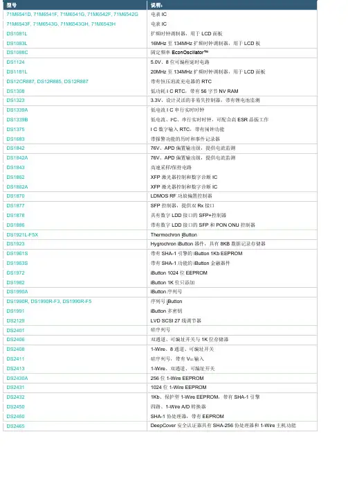
HMC121G8中文资料
- 格式:pdf
- 大小:107.50 KB
- 文档页数:6
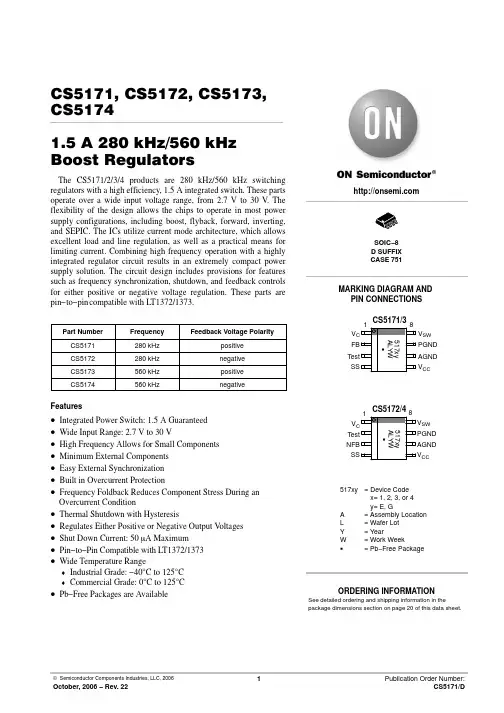
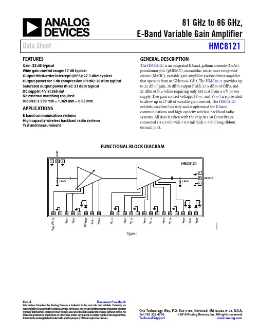
81 GHz to 86 GHz,E-Band Variable Gain AmplifierData SheetHMC8121Rev. A Document Feedback Information furnished by Analog Devices is believed to be accurate and reliable. However , no responsibility is assumed by Analog Devices for its use, nor for any infringements of patents or other rights of third parties that may result from its use. Specifications subject to change without notice. No license is granted by implication or otherwise under any patent or patent rights of Analog Devices. T rademarks and registered trademarks are the property of their respective owners.One Technology Way, P.O. Box 9106, N orwood, MA 02062-9106, U.S.A.Tel: 781.329.4700 ©2016 Analog Devices, Inc. All rights reserved. Technical Support FEATURESGain: 22 dB typicalWide gain control range: 17 dB typicalOutput third-order intercept (OIP3): 27.5 dBm typicalOutput power for 1 dB compression (P1dB): 20 dBm typical Saturated output power (P SAT ): 21 dBm typical DC supply: 4 V at 265 mANo external matching requiredDie size: 3.599 mm × 1.369 mm × 0.05 mmAPPLICATIONSE-band communication systemsHigh capacity wireless backhaul radio systems Test and measurementGENERAL DESCRIPTIONThe HMC8121 is an integrated E-band, gallium arsenide (GaAs), pseudomorphic (pHEMT), monolithic microwave integrated circuit (MMIC), variable gain amplifier and/or driver amplifier that operates from 81 GHz to 86 GHz. The HMC8121 provides up to 22 dB of gain, 20 dBm output P1dB, 27.5 dBm of OIP3, and 21 dBm of P SAT while requiring only 265 mA from a 4 V power supply. Two gain control voltages (V CTL1 and V CTL2) are provided to allow up to 17 dB of variable gain control. The HMC8121 exhibits excellent linearity and is optimized for E-band communications and high capacity wireless backhaul radio systems. All data is taken with the chip in a 50 Ω test fixture connected via a 3 mil wide × 0.5 mil thick × 7 mil long ribbon on each port.FUNCTIONAL BLOCK DIAGRAMF I NV G G 1/V G G V D D 1V D D 2E N V D E TV C T L 1V C T L 2V G G V D D 3V G G V D D 4V G G V G G V D D 5V D D 6V R E FV D E TRFOUT13154-001Figure 1.HMC8121Data SheetRev. A | Page 2 of 16TABLE OF CONTENTSFeatures .............................................................................................. 1 Applications ....................................................................................... 1 General Description ......................................................................... 1 Functional Block Diagram .............................................................. 1 Revision History ............................................................................... 2 Specifications ..................................................................................... 3 Absolute Maximum Ratings ............................................................ 4 Thermal Resistance ...................................................................... 4 ESD Caution .................................................................................. 4 Pin Configuration and Function Descriptions ............................. 5 Interface Schematics..................................................................... 6 Typical Performance Characteristics ..............................................7 Theory of Operation ...................................................................... 12 Typical Application Circuit ........................................................... 13 Assembly Diagram ..................................................................... 14 Mounting and Bonding Techniques for Millimeterwave GaAs MMICs ............................................................................................. 15 Handling Precautions ................................................................ 15 Mounting ..................................................................................... 15 Wire Bonding .............................................................................. 15 Outline Dimensions ....................................................................... 16 Ordering Guide .. (16)REVISION HISTORY2/16—Revision A: Initial VersionData SheetHMC8121Rev. A | Page 3 of 16SPECIFICATIONST A = 25°C, V DDx = 4 V , V CTLx = −5 V , unless otherwise noted. Table 1.ParameterMin Typ Max Unit OPERATING CONDITIONS RF Frequency Range 81 86 GHz PERFORMANCE Gain19 22 dB Gain Variation over Temperature 0.03 dB/°C Gain Control Range12 17 dB Output Power for 1 dB Compression (P1dB) 16 20 dBm Saturated Output Power (P SAT )21 dBm Output Third-Order Intercept (OIP3) at Maximum Gain 1 27.5 dBm Input Return Loss 12 dB Output Return Loss 10 dB POWER SUPPLYTotal Supply Current (I DD )2265 mA1 Data taken at power input (P IN ) = −10 dBm/tone, 1 MHz spacing.2Set V CTL1/V CTL2 = −5 V and then adjust V GG1/V GG2, V GG3, V GG4, V GG5, and V GG6 from −2 V to 0 V to achieve a total drain current (I DD ) = 265 mA.HMC8121Data SheetRev. A | Page 4 of 16ABSOLUTE MAXIMUM RATINGSTable 2.ParameterRating Drain Bias Voltage (V DD1 to V DD6)4.5 VGate Bias Voltage (V GG1/V GG2, V GG3 to V GG6) −3 V to 0 V Gain Control Voltage (V CTL1 and V CTL2)−6 V to 0 V Maximum Junction Temperature (to Maintain 1 Million Hours Mean Time to Failure (MTTF)) 175°CStorage Temperature Range −65°C to +150°C Operating Temperature Range−55°C to +85°CStresses at or above those listed under Absolute Maximum Ratings may cause permanent damage to the product. This is a stress rating only; functional operation of the product at these or any other conditions above those indicated in the operational section of this specification is not implied. Operation beyond the maximum operating conditions for extended periods may affect product reliability.THERMAL RESISTANCETable 3. Thermal ResistancePackage TypeθJC 1 Unit 28-Pad Bare Die [CHIP]69.5 °C/W1Based on ABLEBOND® 84-1LMIT as die attach epoxy with thermal conductivity of 3.6 W/mK.ESD CAUTIONData SheetHMC8121Rev. A | Page 5 of 16PIN CONFIGURATION AND FUNCTION DESCRIPTIONS28272625242322212019181716151413121110987R F I NV G G 1/V G G 2V D D 1V D D 2E N V D E TV C T L 1V C T L 2V G G 3V D D 3V G G 4V D D 4V G G 5V G G 6V D D 5V D D 6V R E FV D E T123456RFOUT GND GNDG N DG N DG N DG N DG N DG N DG N DG N DHMC8121TOP VIEW (Not to Scale)13154-002Figure 2. Pad ConfigurationTable 4. Pad Function DescriptionsPad No. Mnemonic Description1, 3, 4, 6, 10, 13, 16, 19, 24, 27 GND Ground Connection (See Figure 3).2 RFIN RF Input. DC couple RFIN and match it to 50 Ω (see Figure 4). 5 RFOUT RF Output. DC couple RFOUT and match it to 50 Ω (see Figure 5).7 V DETDetector Voltage for the Power Detector (See Figure 6). V DET is the dc voltage representing the RF output power rectified by the diode, which is biased through an external resistor. Refer to the typical application circuit for the required external components (see Figure 38).8 V REFReference Voltage for the Power Detector (See Figure 6). V REF is the dc bias of the diode biased through an external resistor used for the temperature compensation of V DET . Refer to the typical application circuit for the required external components (see Figure 38).9, 12, 15, 18, 25, 26 V DD6 to V DD1 Drain Bias Voltage for the Variable Gain Amplifier (See Figure 7). For the required external components, see Figure 38.11, 14, 17, 20, 28 V GG6 to V GG3, V GG1/V GG2 Gate Bias Voltage for the Variable Gain Amplifier (See Figure 8). For the required external components, see Figure 38.21, 22V CTL2, V CTL1Gain Control Voltage for the Variable Gain Amplifier (See Figure 9). For the required external components, see Figure 38.23 ENV DET Envelope Detector (See Figure 10). For the required external components, see Figure 38. Die Bottom GNDGround. Die bottom must be connected to the RF/dc ground (see Figure 3).HMC8121Data SheetRev. A | Page 6 of 16INTERFACE SCHEMATICS13154-003Figure 3. GND InterfaceRFIN13154-004Figure 4. RFIN InterfaceRFOUT13154-005Figure 5. RFOUT InterfaceDET , V REF13154-006Figure 6. V DET , V REF InterfaceV DD6, V DD5, V DD4,V , V , V DD113154-007Figure 7. V DD6 to V DD1 InterfaceV GG6GG3,V GG1/V GG213154-008Figure 8. V GG6 to V GG3, V GG1/V GG2 InterfaceV CTL2CTL113154-009Figure 9. V CTL2, V CTL1 InterfaceDET13154-010Figure 10. ENV DET InterfaceData SheetHMC8121Rev. A | Page 7 of 16TYPICAL PERFORMANCE CHARACTERISTICSR E S P O N S E (d B )FREQUENCY (GHz)–30–20–1010203013154-011Figure 11. Broadband Gain and Return Loss Response vs. Frequency,V CTL1/V CTL2 = −5 V051015202530G A I N (d B )FREQUENCY (GHz)13154-012Figure 12. Gain vs. Frequency at Various Control Voltages–24–20–16–12–8–40R E T U R N L O S S (d B )FREQUENCY (GHz)81.081.582.082.583.083.584.084.585.085.586.013154-013Figure 13. Input Return Loss vs. Frequency at Various Temperatures,VCTL1/V CTL2 = −5 V 1012141618202224262830G A I N (d B )FREQUENCY (GHz)13154-014Figure 14. Gain vs. Frequency at Various Temperatures,V CTL1/V CTL2 = −5 V051015202530G A I N (d B )CONTROL VOLTAGE (V)13154-015Figure 15. Gain vs. Control Voltage at Various RF Frequencies–24–20–16–12–8–4R E T U R N L O S S (d B )FREQUENCY (GHz)13154-016Figure 16. Output Return Loss vs. Frequency at Various Temperatures,V CTL1/V CTL2 = −5 VHMC8121Data SheetRev. A | Page 8 of 16–30–25–20–15–10–50R E T U R N L O S S (d B )FREQUENCY (GHz)13154-017Figure 17. Input Return Loss vs. Frequency at Various Control Voltages–70–65–60–55–50–45–40I S O L A T I O N (d B )FREQUENCY (GHz)81.081.582.082.583.083.584.084.585.085.586.013154-033Figure 18. Reverse Isolation vs. Frequency at Various Temperatures,V CTL1/V CTL2 = −5 V1516171819202122232425P 1d B (d B m )FREQUENCY (GHz)13154-018Figure 19. Output P1dB vs. Frequency at Various Temperatures,V CTL1/V CTL2= −5 V –24–20–16–12–8–4R E T U R N L O S S (d B )FREQUENCY (GHz)81.081.582.082.583.083.584.084.585.085.586.013154-020Figure 20. Output Return Loss vs. Frequency at Various Control Voltages2021222324252627282930I P 3 (d B m )FREQUENCY (GHz)13154-019Figure 21. Output IP3 vs. Frequency at Various Temperatures,PIN = −10 dBm/Tone, V CTL1/V CTL2 = −5 V151617181920212223242581.081.582.082.583.083.584.084.585.085.586.0P S A T (d B m )FREQUENCY (GHz)13154-021Figure 22. P SAT vs. Frequency at Various Temperatures,V CTL1/V CTL2 = −5 VData SheetHMC8121Rev. A | Page 9 of 16048121620242832–5.0–4.5–4.0–3.5–3.0–2.5–2.0–1.5–1.0G A I N (d B ), I P 3(d B m )CONTROL VOLTAGE (V)13154-022Figure 23. Gain and Input/Output IP3 vs. Control Voltage,P IN = −10 dBm/Tone, RF = 81 GHz048121620242832G A I N (d B ), I P 3 (d B m )CONTROL VOLTAGE (V)13154-023Figure 24. Gain and Input/Output IP3 vs. Control Voltage,P IN = −10 dBm/Tone, RF = 83.5 GHz048121620242832G A I N (d B ), I P 3 (d B m )CONTROL VOLTAGE (V)13154-026Figure 25. Gain and Input/Output IP3 vs. Control Voltage,P IN = −10 dBm/Tone, RF = 86 GHz–20–15–10–5051015252085105125145165185205225245265G A I N (d B ), I P 3 (d B m )DRAIN CURRENT (mA)13154-024Figure 26. Gain and Input/Output IP3 vs. Drain Current, P IN = −5 dBm/Tone, V CTL1/V CTL2 = −1 V, RF = 81 GHz,Drain Current = (I DD1/I DD2 Fixed at 50 mA) + (I DD3 to I DD6 Swept)–20–15–10–5051015252085105125145165185205225245265G A I N (d B ), I P 3 (d B m )DRAIN CURRENT (mA)13154-027Figure 27. Gain and Input/Output IP3 vs. Drain Current, P IN = −5 dBm/Tone, V CTL1/V CTL2 = −1 V, RF = 83.5 GHz, Drain Current = (I DD1/I DD2 Fixed at 50 mA) + (I DD3 to I DD6 Swept)–20–15–10–5051015252085105125145165185205225245265G A I N (d B ), I P 3 (d B m )DRAIN CURRENT (mA)13154-025Figure 28. Gain and Input/Output IP3 vs. Drain Current, P IN = −5 dBm/Tone, V CTL1/V CTL2 = −1 V, RF = 86 GHz,Drain Current = (I DD1/I DD2 Fixed at 50 mA) + (I DD3 to I DD6 Swept)HMC8121Data SheetRev. A | Page 10 of 16–20–15–10–50510G A I N (d B )FREQUENCY (GHz)13154-028Figure 29. Gain vs. Frequency at Various Drain Currents,P IN = −5 dBm/Tone, V CTL1/V CTL2 = −1 V,Drain Current = (I DD1/I DD2 fixed at 50 mA) + (I DD3 to IDD6 Swept)23025027029031033035004812162024I D D (m A )P O U T (d B m ), G A I N (d B ),P A E (%)INPUT POWER (dBm)13154-032Figure 30. P OUT , Gain, PAE, and I DD vs. Input Power,V CTL1/V CTL2 = −5 V, RF = 83.5 GHz0.0010.010.1110V R E F – V D E T (V )OUTPUT POWER (dBm)13154-031Figure 31. Detector Output Voltage (V REF – V DET ) vs. Output Power atVarious RF Frequencies, V CTL1/V CTL2= −5 V23025027029031033035004812162024–15–13–11–9–7–5–3–113I D D (m A )P O U T (d B m ), G A I N (d B ),P A E (%)INPUT POWER (dBm)13154-029Figure 32. P OUT , Gain, PAE, and I DD vs. Input Power,V CTL1/V CTL2= −5 V, RF = 81 GHz23025027029031033035004812162024I D D (m A )P O U T (d B m ), G A I N (d B ),P A E (%)INPUT POWER (dBm)13154-030Figure 33. P OUT , Gain, PAE, and I DD vs. Input Power,V CTL1/V CTL2 = −5 V, RF = 86 GHz00.050.100.150.200.250.300.350.40–20–18–16–14–12–10–8–6–4P E A K -T O -P E A K O U T P U T V O L T A G E (V )TOTAL INPUT POWER (dBm)13154-134Figure 34. Envelope Detector Peak-to-Peak Output Voltage vs. Total InputPower at Various Tone Spacings, RF = 81 GHz, V CTL1/V CTL2 = −5 V,V DET = 4 V with 150 Ω Load Impedance at ENV DET00.050.100.150.200.250.300.350.40–20–18–16–14–12–10–8–6–4P E A K -T O -P E A K O U T P U T V O L T A G E (V )TOTAL INPUT POWER (dBm)13154-135Figure 35. Envelope Detector Peak-to-Peak Output Voltage vs. Total InputPower at Various Tone Spacings, RF = 83.5 GHz, V CTL1/V CTL2 = −5 V,V DET = 4 V with 150 Ω Load Impedance at ENV DET 00.050.100.150.200.250.300.350.40–20–18–16–14–12–10–8–6–4P E A K -T O -P E A K O U T P U T V O L T A G E (V )TOTAL INPUT POWER (dBm)13154-136Figure 36. Envelope Detector Peak-to-Peak Output Voltage vs. Total InputPower at Various Tone Spacings, RF = 86 GHz, V CTL1/V CTL2 = −5 V,V DET = 4 V with 150 Ω Load Impedance at ENV DETTHEORY OF OPERATIONThe circuit architecture of the HMC8121 variable gain amplifier is shown in Figure 37. The HMC8121 uses multiple gain stages and staggered voltage variable attenuation stages to form a low noise, high linearity variable gain amplifier with a gain range of ~17 dB. The first stage is a low noise preamp, which is followed by the first voltage variable attenuator in the signal path. A portion of the signal is coupled away and further amplified before driving an on-chip envelope detector. The envelope detector provides an output that is proportional to the peak envelope power of the incoming signal. After the first attenuator, a second stage amplifier provides additional gain and isolation before driving the second variable attenuator block. Three cascaded gain stages follow the second variable attenuator. At the output of the last stage, another coupler taps off a small portion of the output signal. The coupled signal is presented to an on-chip diode detector for external monitoring of the output power. A matched reference diode is included to help correct for detector temperature dependencies. See the application circuit in Figure 38 for further details on biasing the different blocks and utilizing the detector features.RFIN RFOUTDET CTL1CTL2REF DET13154-034Figure 37. Variable Gain Amplifier Circuit ArchitectureTYPICAL APPLICATION CIRCUITA typical application circuit for the HMC8121 is provided in Figure 38. For typical operation, drive the attenuator control pads from a single control voltage. It is important to bypass all the supply connections and attenuator control pads withadequate bypassing capacitors. Use single-layer chip capacitors with very high self-resonant frequency close to the HMC8121 die, bypassing each supply or control pad. Typically, 120 pF chip capacitors are used, followed by 0.01 μF and 4.7 μF surface-mount capacitors. Combine supply lines as shown in the application circuit schematic to minimize external component count and simplify power supply routing (see Figure 38). Pad 25 and Pad 26 are internally connected. Therefore, use either pad to connect the external bypass components of V DD1/V DD2. The HMC8121 uses several amplifier, detector, and attenuator stages. All stages use depletion mode pHEMT transistors. It is important to follow the following power-up bias sequence to ensure transistor damage does not occur. 1. Apply a −5 V bias to the V CTL1 and V CTL2 pads.2. Apply a −2 V bias to the V GG3 to V GG6 and V GG1/V GG2 pads.3. Apply 4 V to the V DD1 to V DD6 pads.4.Adjust V GG1/V GG2 and V GG3 to V GG6 between −2 V and 0 V to achieve a total amplifier drain current of 265 mA.After bias is established, adjust the V CTL1 = V CTL2 bias between −5 V and 0 V to achieve the desired gain.To power down the HMC8121, follow the reverse procedure. For additional guidance on general bias sequencing, see the MMIC Amplifier Biasing Procedure application note.F I N13154-035Figure 38. Typical Application CircuitASSEMBLY DIAGRAMGG1GG2GG3GG4DD6DD3DD4DD5GG5GG6DD1DD2CTL1CTL213154-036Figure 39. Assembly DiagramMOUNTING AND BONDING TECHNIQUES FOR MILLIMETERWAVE GaAs MMICSAttach the die directly to the ground plane eutectically or with conductive epoxy.To bring RF to and from the chip, use 50 Ω microstrip trans-mission lines on 0.127 mm (5 mil) thick alumina thin film substrates (see Figure 40).13154-037Figure 40. Routing RF SignalsTo minimize bond wire length, place microstrip substrates as close to the die as possible. Typical die to substrate spacing is 0.076 mm to 0.152 mm (3 mil to 6 mil).HANDLING PRECAUTIONSTo avoid permanent damage, adhere to the following precautions.StorageAll bare die ship in either waffle or gel-based ESD protective containers, sealed in an ESD protective bag. After opening the sealed ESD protective bag, all die must be stored in a dry nitrogen environment.CleanlinessHandle the chips in a clean environment. Never use liquid cleaning systems to clean the chip.Static SensitivityFollow ESD precautions to protect against ESD strikes. TransientsSuppress instrument and bias supply transients while bias is applied. To minimize inductive pickup, use shielded signal and bias cables.General HandlingHandle the chip on the edges only using a vacuum collet or with a sharp pair of bent tweezers. Because the surface of the chip has fragile air bridges, never touch the surface of the chip with a vacuum collet, tweezers, or fingers.MOUNTINGThe chip is back metallized and can be die mounted with gold/tin (AuSn) eutectic preforms or with electrically conductive epoxy. The mounting surface must be clean and flat.Eutectic Die AttachIt is best to use an 80% gold/20% tin preform with a work surface temperature of 255°C and a tool temperature of 265°C. When hot 90% nitrogen/10% hydrogen gas is applied, maintain tool tip temperature at 290°C. Do not expose the chip to a temperature greater than 320°C for more than 20 sec. No more than 3 sec of scrubbing is required for attachment.Epoxy Die AttachABLEBOND 84-1LMIT is recommended for die attachment. Apply a minimum amount of epoxy to the mounting surface so that a thin epoxy fillet is observed around the perimeter of the chip after placing it into position. Cure the epoxy per the schedule provided by the manufacturer.WIRE BONDINGRF bonds made with 0.003 in. × 0.0005 in. gold ribbon are recom-mended for the RF ports. These bonds must be thermosonically bonded with a force of 40 g to 60 g. DC bonds of 0.001 in.(0.025 mm) diameter, thermosonically bonded, are recommended. Create ball bonds with a force of 40 g to 50 g and wedge bonds with a force of 18 g to 22 g. Create all bonds with a nominal stage temperature of 150°C. Apply a minimum amount of ultrasonic energy to achieve reliable bonds. Keep all bonds as short as possible, less than 12 mil (0.31 mm).OUTLINE DIMENSIONS01-26-2016-AFigure 41. 28-Pad Bare Die [CHIP](C-28-1)Dimensions shown in millimetersORDERING GUIDEModel 1 Temperature Range Package Description Package Option 2 HMC8121 −55°C to +85°C 28-Pad Bare Die [CHIP] C-28-1 HMC8121-SX−55°C to +85°C 28-Pad Bare Die [CHIP] C-28-11 The HMC8121-SX is two pairs of the die in a gel pack for the sample orders.2This is a waffle pack option; contact Analog Devices, Inc., sales representatives for additional packaging options.©2016 Analog Devices, Inc. All rights reserved. Trademarks and registered trademarks are the property of their respective owners. D13154-0-2/16(A)。
部分分立元件库元件名称及中英对照AND ------------------------------------与门ANTENNA --------------------------------天线BA TTERY --------------------------------直流电源BELL -----------------------------------铃,钟BVC ------------------------------------同轴电缆接插件BRIDEG 1 -------------------------------整流桥(二极管) BRIDEG 2 -------------------------------整流桥(集成块) BUFFER--------------------------------- 缓冲器BUZZER----------------------------------蜂鸣器CAP ------------------------------------电容CAPACITOR ------------------------------电容CAPACITOR POL --------------------------有极性电容CAPV AR ---------------------------------可调电容CIRCUIT BREAKER ------------------------熔断丝COAX -----------------------------------同轴电缆CON ------------------------------------插口CRYSTAL --------------------------------晶体整荡器DB --------------------------------------并行插口DIODE ---------------------------------二极管DIODE SCHOTTKY ------------------------稳压二极管DIODE V ARACTOR ------------------------变容二极管DPY_3-SEG---------------------------- 3段LEDDPY_7-SEG---------------------------- 7段LEDDPY_7-SEG_DP -------------------------7段LED(带小数点) ELECTRO ------------------------------电解电容FUSE ----------------------------------熔断器INDUCTOR -----------------------------电感INDUCTOR IRON -------------------------带铁芯电感INDUCTOR3 -----------------------------可调电感JFET N -------------------------------N沟道场效应管JFET P --------------------------------P沟道场效应管LAMP ----------------------------------灯泡LAMP NEDN -----------------------------起辉器LED -----------------------------------发光二极管METER ---------------------------------仪表MICROPHONE ----------------------------麦克风MOSFET --------------------------------MOS管MOTOR AC -----------------------------交流电机MOTOR SERVO --------------------------伺服电机NAND ----------------------------------与非门NOR ----------------------------------或非门NOT -----------------------------------非门NPN -----------------------------------NPN----三极管NPN-PHOTO ------------------------------感光三极管OPAMP ----------------------------------运放OR ------------------------------------或门PHOTO ---------------------------------感光二极管PNP -----------------------------------三极管NPN DAR ----------------------------NPN三极管PNP DAR ----------------------------PNP三极管POT ----------------------------滑线变阻器PELAY-DPDT---------------------------- 双刀双掷继电器RES1.2 ----------------------------电阻RES3.4 ----------------------------可变电阻RESISTOR BRIDGE ? ----------------------------桥式电阻RESPACK ? ----------------------------电阻SCR ----------------------------晶闸管PLUG ?---------------------------- 插头PLUG AC FEMALE---------------------------- 三相交流插头SOCKET ? ----------------------------插座SOURCE CURRENT---------------------------- 电流源SOURCE VOLTAGE ----------------------------电压源SPEAKER ----------------------------扬声器SW ? ----------------------------开关SW-DPDY ?---------------------------- 双刀双掷开关SW-SPST ? ----------------------------单刀单掷开关SW-PB ----------------------------按钮THERMISTOR ----------------------------电热调节器TRANS1 ----------------------------变压器TRANS2 ----------------------------可调变压器TRIAC ?---------------------------- 三端双向可控硅TRIODE ? ----------------------------三极真空管V ARISTOR ----------------------------变阻器ZENER ? ----------------------------齐纳二极管DPY_7-SEG_D---------------------------- 数码管SW-PB ---------------------------- 开关7805----------------------------------LM7805CT。
内部特点:-高性能、低功耗的 8 位AVR 微处理器-先进的RISC 结构-130 条指令–大多数指令执行时间为单个时钟周期-32个8 位通用工作寄存器-全静态工作-工作于16 MHz 时性能高达16 MIPS-只需两个时钟周期的硬件乘法器-非易失性程序和数据存储器-8K 字节的系统内可编程Flash-擦写寿命:10,000 次-具有独立锁定位的可选Boot 代码区-通过片上Boot 程序实现系统内编程-真正的同时读写操作-512 字节的EEPROM-1K字节的片内SRAM-可以对锁定位进行编程以实现用户程序的加密外设特点:–两个具有独立预分频器8 位定时器/ 计数器, 其中之一有比较功能–一个具有预分频器、比较功能和捕捉功能的16 位定时器/ 计数器–具有独立振荡器的实时计数器RTC–三通道PWM– TQFP与MLF 封装的8 路ADC-8 路10 位ADC– PDIP封装的6 路ADC –面向字节的两线接口–两个可编程的串行USART–可工作于主机/ 从机模式的SPI 串行接口–具有独立片内振荡器的可编程看门狗定时器–片内模拟比较器· 特殊的处理器特点–上电复位以及可编程的掉电检测–片内经过标定的RC 振荡器–片内/ 片外中断源– 5种睡眠模式: 空闲模式、ADC 噪声抑制模式、省电模式、掉电模式及Standby 模式· I/O 和封装– 23个可编程的I/O 口状态; ADC 噪声抑制模式时终止CPU 和除了异步定时器与ADC 以外所有I/O 模块的工作,以降低ADC 转换时的开关噪声; Standby 模式下只有晶体或谐振振荡器运行,其余功能模块处于休眠状态,使得器件只消耗极少的电流,同时具有快速启动能力。
本芯片是以Atmel 高密度非易失性存储器技术生产的。
片内ISP Flash 允许程序存储器通过ISP 串行接口,或者通用编程器进行编程,也可以通过运行于AVR 内核之中的引导程序进行编程。
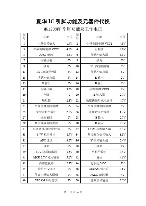
夏华IC引脚功能及元器件代换M61208FP引脚功能及工作电压
J系列CPU(SDA555X)各脚功能及电压
TDA16846功能脚简介
STR-G5653引脚功能及电压
ST6378引脚功能
TDA6210Q引脚功能
AN7583引脚功能
TA8720AN AV开关
SDA9380引脚功能
TDA8362引脚功能
厦华彩电各型号中周内置电容值
厦华彩电显像管、高压包及电路主要参数对照表(一)
第10 页共30 页
第11 页共30 页
第12 页共30 页
第13 页共30 页
第14 页共30 页
第15 页共30 页
第16 页共30 页
第17 页共30 页
第18 页共30 页
第19 页共30 页
厦华彩电行包代换表
第20 页共30 页
第21 页共30 页
第22 页共30 页
第23 页共30 页
第24 页共30 页
第25 页共30 页
开关变压器代用表
1/2W稳压管型号稳压值
场效应管K3116可用K2645代用。
D400可用C2344代用。
C2344可用C5248代用厦华彩电机型与CPU型号对应表。

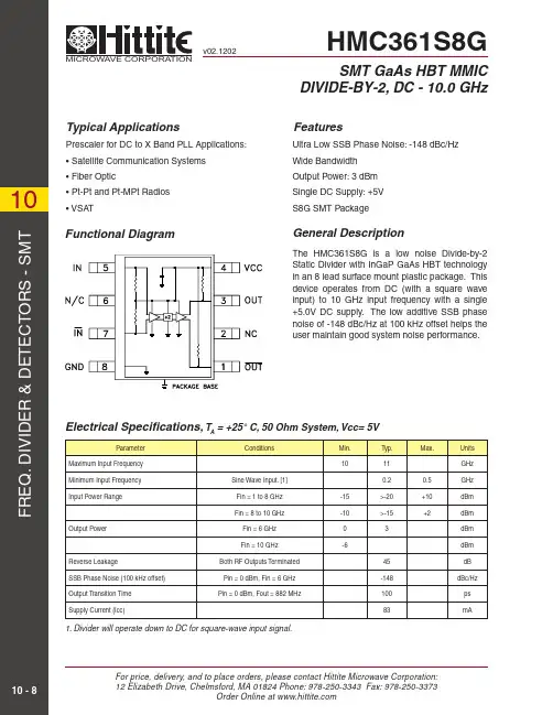
THIS PAGE INTENTIONALLY LEFT BLANK4For price, delivery and to place orders: Hittite Microwave Corporation, 20 Alpha Road, Chelmsford, MA 01824Phone: 978-250-3343 Fax: 978-250-3373 Order On-line at ApplicationSupport:Phone:******************************General Description Functional Diagram The HMC365G8 is a low noise Divide-by-4 Static Divider with InGaP GaAs HBT technology in an 8 lead glass/metal (hermetic) surface mount hermetic package. This device operates from DC (with a square wave input) to 13 GHz input frequency with a single +5V DC supply. The low additive SSB phase noiseof -151 dBc/Hz at 100 kHz offset helps the user maintain good system noise performance.Ultra Low SSB Phase Noise: -151 dBc/Hz Wide Bandwidth Output Power: 7 dBm Single DC Supply: +5V 8 Lead Hermetic SMT Package Electrical Specifications, T A = +25° C, 50 Ohm System, Vcc = 5VPrescaler for DC to Ku Band PLL Applications:• Point-to-Point / Multi-Point Radios• VSAT Radios • Fiber Optic • Test Equipment • Space & Military1. Divider will operate down to DC for square-wave input signal.F R E Q U E N C Y D I V I D E R S & D E T E C T O R S - S M T 44 - 2For price, delivery and to place orders: Hittite Microwave Corporation, 20 Alpha Road, Chelmsford, MA 01824Phone: 978-250-3343 Fax: 978-250-3373 Order On-line at ApplicationSupport:Phone:******************************-30-20-100102001234567891011121314151617I N P U T P O W E R (d B m )INPUT FREQUENCY (GHz)-30-20-100102001234567891011121314151617Min Pin + 25C Max Pin + 25CMin Pin + 85CMax Pin + 85CMin Pin -40CMax Pin -40CI N P U T P O W E R (d B m )INPUT FREQUENCY (GHz)SSB Phase NoisePerformance, Pin= 0 dBm, T= 25 °C Output Power vs. Temperature Reverse Leakage, Pin= 0 dBm, T= 25 °COutput Harmonic Content, Pin= 0 dBm, T= 25 °C -160-140-120-100-80-60-40-200102103104105106107S S BP HASEN OIS E(dB c /H z)OFFSET FREQUENCY (Hz)-60-50-40-30-20-10003691215Both Output Ports Terminated One Output Port Terminated POW ERLE VEL(d Bm )INPUT FREQUENCY (GHz)-50-40-30-20-10003691215Pfeedthru 2nd Harmonic 3rd Harmonic O U T P U T L E V E L (d B m )INPUT FREQUENCY (GHz)024681003691215+ 25C + 85C - 40C O U T P U T P O W E R (d B m )INPUT FREQUENCY (GHz)4For price, delivery and to place orders: Hittite Microwave Corporation, 20 Alpha Road, Chelmsford, MA 01824Phone: 978-250-3343 Fax: 978-250-3373 Order On-line at ApplicationSupport:Phone:******************************Outline DrawingNote: Divider will operate over full voltage range shown above Typical Supply Current vs. Vcc3. PLATING: ELECTROLYTIC GOLD 50 MICROINCHES MIN., OVERELECTROLYTIC NICKEL 50 MICROINCHES MIN.4. DIMENSIONS ARE IN INCHES [MILLIMETERS].5. TOLERANCES: ±.005 [0.13] UNLESS OTHERWISE SPECIFIED.6. ALL GROUND LEADS AND GROUND PADDLE MUST BE SOLDERED TO PCB RF GROUND.ELECTROSTATIC SENSITIVE DEVICE OBSERVE HANDLING PRECAUTIONS -700-500-300-10010030050070022.723.123.523.924.324.7A M P L I T U D E (m V )TIME (nS)F R E Q U E N C Y D I V I D E R S & D E T E C T O R S - S M T 44 - 4For price, delivery and to place orders: Hittite Microwave Corporation, 20 Alpha Road, Chelmsford, MA 01824Phone: 978-250-3343 Fax: 978-250-3373 Order On-line at ApplicationSupport:Phone:******************************4For price, delivery and to place orders: Hittite Microwave Corporation, 20 Alpha Road, Chelmsford, MA 01824Phone: 978-250-3343 Fax: 978-250-3373 Order On-line at ApplicationSupport:Phone:******************************The circuit board used in the application should use RF circuit design techniques. Signal lines should have 50 Ohm impedance while the package ground leads and backside ground slug should be con-nected directly to the ground plane similar to that shown. A sufficient number of via holes should be used to connect the top and bottom ground planes.The evaluation circuit board shown is availablefrom Hittite upon request. This evaluation board isdesigned for single ended input testing. J2 and J3provide differential output signals.[1] Reference this number when ordering complete evaluation PCB[2] Circuit Board Material: Rogers 4350List of Materials for Evaluation PCB 106582 [1]F R E Q U E N C Y D I V I D E R S & D E T E C T O R S - S M T 44 - 6For price, delivery and to place orders: Hittite Microwave Corporation, 20 Alpha Road, Chelmsford, MA 01824Phone: 978-250-3343 Fax: 978-250-3373 Order On-line at ApplicationSupport:Phone:******************************。