D44TD5中文资料
- 格式:pdf
- 大小:127.95 KB
- 文档页数:2
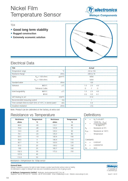
MJD44H11,NJVMJD44H11 (NPN), MJD45H11,NJVMJD45H11 (PNP) Complementary Power TransistorsDPAK For Surface Mount Applications Designed for general purpose power and switching such as output or driver stages in applications such as switching regulators, converters, and power amplifiers.Features•Lead Formed for Surface Mount Application in Plastic Sleeves (No Suffix)•Straight Lead Version in Plastic Sleeves (“−1” Suffix)•Electrically Similar to Popular D44H/D45H Series•Low Collector Emitter Saturation V oltage −V CE(sat) = 1.0 V olt Max @ 8.0 A•Fast Switching Speeds•Complementary Pairs Simplifies Designs•Epoxy Meets UL 94 V−0 @ 0.125 in•ESD Ratings:Human Body Model, 3B u 8000 VMachine Model, C u 400 V•NJV Prefix for Automotive and Other Applications Requiring Unique Site and Control Change Requirements; AEC−Q101 Qualified and PPAP Capable•These are Pb−Free Packages**For additional information on our Pb−Free strategy and soldering details, please download the ON Semiconductor Soldering and Mounting Techniques Reference Manual, SOLDERRM/D.SILICONPOWER TRANSISTORS8 AMPERES80 VOLTS, 20 WATTSIPAKCASE 369DSTYLE 1DPAKCASE 369CSTYLE 1MARKINGDIAGRAMSA=Assembly LocationY YearWW Work WeekJ4xH11=Device Codex = 4 or 5G=Pb−Free PackageAYWWJ4xH11GSee detailed ordering and shipping information in the package dimensions section on page 7 of this data sheet.ORDERING INFORMATIONMAXIMUM RATINGS (T A= 25_C, common for NPN and PNP, minus sign, “−”, for PNP omitted, unless otherwise noted)Rating Symbol Max Unit Collector−Emitter Voltage V CEO80Vdc Emitter−Base Voltage V EB5VdcCollector Current− Continuous− Peak I C816AdcTotal Power Dissipation @ T C = 25°CDerate above 25°C P D200.16WW/°CTotal Power Dissipation (Note 1) @ T A = 25°CDerate above 25°C P D1.750.014WW/°COperating and Storage JunctionTemperature RangeT J, T stg−55 to +150°CStresses exceeding Maximum Ratings may damage the device. Maximum Ratings are stress ratings only. Functional operation above the Recommended Operating Conditions is not implied. Extended exposure to stresses above the Recommended Operating Conditions may affect device reliability.THERMAL CHARACTERISTICSCharacteristic Symbol Max Unit Thermal Resistance, Junction−to−Case R q JC 6.25°C/W Thermal Resistance, Junction−to−Ambient (Note 1)R q JA71.4°C/W Lead Temperature for Soldering T L260°C1.These ratings are applicable when surface mounted on the minimum pad sizes recommended.ELECTRICAL CHARACTERISTICS(T A= 25_C, common for NPN and PNP, minus sign, “−”, for PNP omitted, unless otherwise noted)Characteristic Symbol Min Typ Max Unit OFF CHARACTERISTICSCollector−Emitter Sustaining Voltage(I C = 30 mA, I B = 0)V CEO(sus)80VdcCollector Cutoff Current(V CE = Rated V CEO, V BE = 0)I CES 1.0m AEmitter Cutoff Current(V EB = 5 Vdc)I EBO 1.0m A ON CHARACTERISTICSCollector−Emitter Saturation Voltage(I C = 8 Adc, I B = 0.4 Adc)V CE(sat)1VdcBase−Emitter Saturation Voltage(I C = 8 Adc, I B = 0.8 Adc)V BE(sat) 1.5VdcDC Current Gain(V CE = 1 Vdc, I C = 2 Adc)h FE60−DC Current Gain(V CE = 1 Vdc, I C = 4 Adc)40DYNAMIC CHARACTERISTICSCollector Capacitance(V CB = 10 Vdc, f test = 1 MHz)MJD44H11, NJVMJD44H11G,/T4G/RLGMJD45H11, NJVMJD45H11T4G/RLG C cb45130pFGain Bandwidth Product(I C = 0.5 Adc, V CE = 10 Vdc, f = 20 MHz)MJD44H11, NJVMJD44H11G,/T4G/RLGMJD45H11, NJVMJD45H11T4G/RLG f T8590MHzSWITCHING TIMESDelay and Rise Times(I C = 5 Adc, I B1 = 0.5 Adc)MJD44H11, NJVMJD44H11G,/T4G/RLGMJD45H11, NJVMJD45H11T4G/RLG t d + t r300135nsStorage Time(I C = 5 Adc, I B1 = I B2 = 0.5 Adc)MJD44H11, NJVMJD44H11G,/T4G/RLGMJD45H11, NJVMJD45H11T4G/RLG t s500500nsFall Time(I C = 5 Adc, I B1 = I B2 = 0.5 Adc MJD44H11, NJVMJD44H11G,/T4G/RLGMJD45H11, NJVMJD45H11T4G/RLG t f140100nst, TIME (ms)10.010.30.20.07r (t ), E F F E C T I V E T R A N S I E N T T H E R M A L R E S I S T A N C E (N O R M A L I Z E D )0.7Figure 1. Thermal Response0.50.10.050.030.02I C , C O L L E C T O R C U R R E N T (A M P )20V CE , COLLECTOR-EMITTER VOLTAGE (VOLTS)20.550.10.31310Figure 2. Maximum Forward BiasSafe Operating AreaThere are two limitations on the power handling ability of a transistor: average junction temperature and second breakdown. Safe operating area curves indicate I C − V CE limits of the transistor that must be observed for reliable operation; i.e., the transistor must not be subjected to greater dissipation than the curves indicate.The data of Figure 2 is based on T J(pk) = 150_C; T C is variable depending on conditions. Second breakdown pulse limits are valid for duty cycles to 10% provided T J(pk)v 150_C. T J(pk) may be calculated from the data in Figure 1. At high case temperatures, thermal limitations will reduce the power that can be handled to values less than the limitations imposed by second breakdown.25T, TEMPERATURE (°C)2015105P D , P O W E R D I S S I P A T I O N (W A T T S )2.5021.510.5T A T C Figure 3. Power DeratingFigure 4. MJD44H11 DC Current GainFigure 5. MJD45H11 DC Current GainI C , COLLECTOR CURRENT (A)Figure 6. MJD44H11 DC Current GainFigure 7. MJD45H11 DC Current GainFigure 8. MJD44H11 Saturation VoltageV CE(sat)Figure 9. MJD45H11 Saturation VoltageV CE(sat)I C , COLLECTOR CURRENT (A)h F E , D C C U R R E N T G A I NV C E (s a t ), C O L L −E M I T S A T U R A T I O N V O L T A G E (V )I C , COLLECTOR CURRENT (A)101000h F E , D C C U R R E N T G A I NI C , COLLECTOR CURRENT (A)h F E , D C C U R R E N T G A I NI C , COLLECTOR CURRENT (A)101000h F E , D C C U R R E N T G A I N I C , COLLECTOR CURRENT (A)0.10.20.30.40.60.70.8V C E (s a t ), C O L L −E M I T S A T U R A T I O N V O L T A G E (V )0.5Figure 10. MJD44H11 Saturation VoltageV BE(sat)Figure 11. MJD45H11 Saturation VoltageV BE(sat)I C , COLLECTOR CURRENT (A)I C , COLLECTOR CURRENT (A)Figure 12. MJD44H11 Collector SaturationRegionFigure 13. MJD45H11 Collector SaturationRegionI B , BASE CURRENT (mA)I B , BASE CURRENT (mA)Figure 14. MJD44H11 Capacitance Figure 15. MJD45H11 CapacitanceV R , REVERSE VOLTAGE (V)V B E (s a t ), B A S E −E M I T S A T U R A T I O N V O L T A G E (V )V C E , C O L L E C T O R −E M I T T E R V O L T A G E (V )C , C A P A C I T A N C E (p F )0.20.40.60.81.01.21.4V B E (s a t ), B A S E −E M I T S A T U R A T I O N V O L T A G E (V )0.40.20.61.01.41.82.0V C E , C O L L E C T O R −E M I T T E R V O L T A G E (V )0.81.21.6V R , REVERSE VOLTAGE (V)101000C , C A P A C I T A N C E (p F )Figure 16. MJD44H11Current −Gain −Bandwidth Product Figure 17. MJD45H11Current −Gain −Bandwidth ProductI C , COLLECTOR CURRENT (A)I C , COLLECTOR CURRENT (A)f T a u , C U R R E N T −G A I N −B A N D W I D T H P R O D U C Tf T a u , C U R R E N T −G A I N −B A N D W I D T H P R O D U C TORDERING INFORMATIONDevicePackage Type PackageShipping †MJD44H11G DPAK (Pb −Free)369C75 Units / RailNJVMJD44H11G DPAK (Pb −Free)MJD44H11−1G DPAK −3(Pb −Free)369DMJD44H11RLG DPAK (Pb −Free)369C1,800 / Tape & ReelNJVMJD44H11RLG DPAK (Pb −Free)MJD44H11T4G DPAK (Pb −Free)2,500 / Tape & ReelNJVMJD44H11T4G DPAK (Pb −Free)MJD44H11T5G DPAK (Pb −Free)MJD45H11G DPAK (Pb −Free)75 Units / RailMJD45H11−1G DPAK −3(Pb −Free)369D MJD45H11RLG DPAK (Pb −Free)369C1,800 / Tape & ReelNJVMJD45H11RLG DPAK (Pb −Free)MJD45H11T4G DPAK (Pb −Free)2,500 / Tape & ReelNJVMJD45H11T4GDPAK (Pb −Free)†For information on tape and reel specifications, including part orientation and tape sizes, please refer to our Tape and Reel Packaging Specifications Brochure, BRD8011/D.DPAK CASE 369C ISSUE DSTYLE 1:PIN 1.BASE2.COLLECTOR3.EMITTER4.COLLECTORǒmm inchesǓSCALE 3:1*For additional information on our Pb −Free strategy and solderingdetails, please download the ON Semiconductor Soldering and Mounting Techniques Reference Manual, SOLDERRM/D.SOLDERING FOOTPRINT*DIM MIN MAX MIN MAX MILLIMETERSINCHES D 0.2350.245 5.97 6.22E 0.2500.265 6.35 6.73A 0.0860.094 2.18 2.38b 0.0250.0350.630.89c20.0180.0240.460.61b20.0300.0450.76 1.14c 0.0180.0240.460.61e 0.090 BSC 2.29 BSC b30.1800.215 4.57 5.46L4−−−0.040−−− 1.01L 0.0550.070 1.40 1.78L30.0350.0500.89 1.27Z0.155−−−3.93−−−NOTES:1.DIMENSIONING AND TOLERANCING PER ASME Y14.5M, 1994.2.CONTROLLING DIMENSION: INCHES.3.THERMAL PAD CONTOUR OPTIONAL WITHIN DI-MENSIONS b3, L3 and Z.4.DIMENSIONS D AND E DO NOT INCLUDE MOLD FLASH, PROTRUSIONS, OR BURRS. MOLDFLASH, PROTRUSIONS, OR GATE BURRS SHALL NOT EXCEED 0.006 INCHES PER SIDE.5.DIMENSIONS D AND E ARE DETERMINED AT THE OUTERMOST EXTREMES OF THE PLASTIC BODY .6.DATUMS A AND B ARE DETERMINED AT DATUM PLANE H.H 0.3700.4109.4010.41A10.0000.0050.000.13L10.108 REF 2.74 REF L20.020 BSC 0.51 BSC DETAIL AROTATED 90 CW 5EDIM MIN MAX MIN MAX MILLIMETERSINCHES A 0.2350.245 5.97 6.35B 0.2500.265 6.35 6.73C 0.0860.094 2.19 2.38D 0.0270.0350.690.88E 0.0180.0230.460.58F 0.0370.0450.94 1.14G 0.090 BSC 2.29 BSC H 0.0340.0400.87 1.01J 0.0180.0230.460.58K 0.3500.3808.899.65R 0.1800.215 4.45 5.45S 0.0250.0400.63 1.01V 0.0350.0500.89 1.27NOTES:1.DIMENSIONING AND TOLERANCING PER ANSI Y14.5M, 1982.2.CONTROLLING DIMENSION: INCH.Z0.155−−−3.93−−−IPAK CASE 369D ISSUE CSTYLE 1:PIN 1.BASE2.COLLECTOR3.EMITTER4.COLLECTORON Semiconductor and are registered trademarks of Semiconductor Components Industries, LLC (SCILLC). SCILLC owns the rights to a number of patents, trademarks,copyrights, trade secrets, and other intellectual property. A listing of SCILLC’s product/patent coverage may be accessed at /site/pdf/Patent −Marking.pdf. SCILLC reserves the right to make changes without further notice to any products herein. SCILLC makes no warranty, representation or guarantee regarding the suitability of its products for any particular purpose, nor does SCILLC assume any liability arising out of the application or use of any product or circuit, and specifically disclaims any and all liability, including without limitation special, consequential or incidental damages. “Typical” parameters which may be provided in SCILLC data sheets and/or specifications can and do vary in different applications and actual performance may vary over time. All operating parameters, including “Typicals” must be validated for each customer application by customer’s technical experts. SCILLC does not convey any license under its patent rights nor the rights of others. SCILLC products are not designed, intended, or authorized for use as components in systems intended for surgical implant into the body, or other applications intended to support or sustain life, or for any other application in which the failure of the SCILLC product could create a situation where personal injury or death may occur. Should Buyer purchase or use SCILLC products for any such unintended or unauthorized application, Buyer shall indemnify and hold SCILLC and its officers, employees, subsidiaries, affiliates, and distributors harmless against all claims, costs, damages, and expenses, and reasonable attorney fees arising out of, directly or indirectly,any claim of personal injury or death associated with such unintended or unauthorized use, even if such claim alleges that SCILLC was negligent regarding the design or manufacture of the part. SCILLC is an Equal Opportunity/Affirmative Action Employer. This literature is subject to all applicable copyright laws and is not for resale in any manner.PUBLICATION ORDERING INFORMATION分销商库存信息:ONSEMIMJD44H11T4G MJD45H11T4G MJD44H11G MJD45H11G MJD44H11-1G MJD45H11-1G MJD44H11T5G MJD44H11RLG MJD45H11RLG MJD45H11-001MJD44H11-001MJD44H11T4 MJD45H11T4MJD44H11T5。
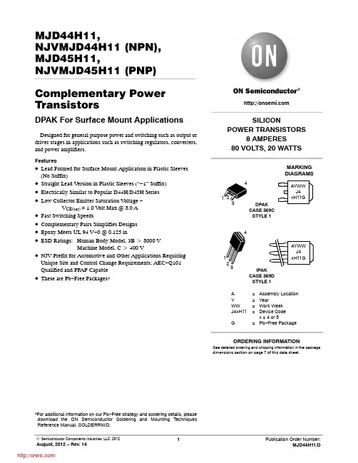
January 2001Si4425DYSingle P-Channel, Logic Level, PowerTrench General Description Features Absolute Maximum Ratings T A = 25o C unless otherwise noted SOT-23SuperSOT TM This P-Channel Logic Level MOSFET is produced using Fairchild Semiconductor's advanced PowerTrench process that has been especially tailored to minimize the on-state resistance and yet maintain low gate charge for superior switching performance.These devices are well suited for notebook computer applications: load switching and power management,battery charging circuits, and DC/DC conversion.SSSSO-8DDD Gpin 14425TRADEMARKSACEx™CoolFET™CROSSVOLT™E 2CMOS TM FACT™FACT Quiet Series™FAST ®FASTr™GTO™HiSeC™The following are registered and unregistered trademarks Fairchild Semiconductor owns or is authorized to use and is not intended to be an exhaustive list of all such trademarks.LIFE SUPPORT POLICYFAIRCHILD’S PRODUCTS ARE NOT AUTHORIZED FOR USE AS CRITICAL COMPONENTS IN LIFE SUPPORTDEVICES OR SYSTEMS WITHOUT THE EXPRESS WRITTEN APPROV AL OF FAIRCHILD SEMICONDUCTOR CORPORA TION.As used herein:ISOPLANAR™MICROWIRE™POP™PowerTrench™QS™Quiet Series™SuperSOT™-3SuperSOT™-6SuperSOT™-8TinyLogic™1. Life support devices or systems are devices or systems which, (a) are intended for surgical implant intothe body, or (b) support or sustain life, or (c) whosefailure to perform when properly used in accordancewith instructions for use provided in the labeling, can be reasonably expected to result in significant injury to the user.2. A critical component is any component of a lifesupport device or system whose failure to perform can be reasonably expected to cause the failure of the life support device or system, or to affect its safety or effectiveness.PRODUCT STATUS DEFINITIONS Definition of Terms Datasheet Identification Product Status DefinitionAdvance InformationPreliminary No Identification Needed Obsolete This datasheet contains the design specifications for product development. Specifications may change in any manner without notice.This datasheet contains preliminary data, andsupplementary data will be published at a later date.Fairchild Semiconductor reserves the right to make changes at any time without notice in order to improve design.This datasheet contains final specifications. Fairchild Semiconductor reserves the right to make changes at any time without notice in order to improve design.This datasheet contains specifications on a product that has been discontinued by Fairchild semiconductor.The datasheet is printed for reference information only.Formative or In DesignFirst ProductionFull ProductionNot In ProductionDISCLAIMERFAIRCHILD SEMICONDUCTOR RESERVES THE RIGHT TO MAKE CHANGES WITHOUT FURTHER NOTICE TO ANY PRODUCTS HEREIN TO IMPROVE RELIABILITY , FUNCTION OR DESIGN. FAIRCHILD DOES NOT ASSUME ANY LIABILITY ARISING OUT OF THE APPLICATION OR USE OF ANY PRODUCT OR CIRCUIT DESCRIBED HEREIN; NEITHER DOES IT CONVEY ANY LICENSE UNDER ITS PATENT RIGHTS, NOR THE RIGHTS OF OTHERS.UHC™VCX™。
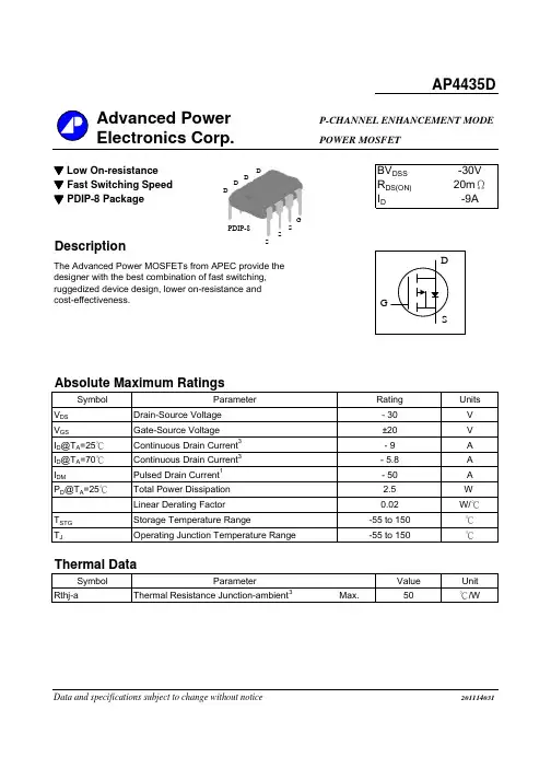
P-CHANNEL ENHANCEMENT MODE POWER MOSFET▼ Low On-resistance BV DSS -30V ▼ Fast Switching Speed R DS(ON)20mΩ▼ PDIP-8 PackageI D-9ADescriptionAbsolute Maximum RatingsSymbol Units V DS V V GSV I D @T A =25℃A I D @T A =70℃A I DMA P D @T A =25℃W W/℃T STG ℃T J℃Symbol Value Unit Rthj-aThermal Resistance Junction-ambient 3Max.50℃/WData and specifications subject to change without noticeThermal DataParameterTotal Power Dissipation 2.5-55 to 150Operating Junction Temperature Range-55 to 150Linear Derating Factor 0.02Storage Temperature RangeContinuous Drain Current 3- 5.8Pulsed Drain Current 1- 50ParameterDrain-Source Voltage Gate-Source Voltage Continuous Drain Current 3201114031AP4435DRating - 30±20- 9The Advanced Power MOSFETs from APEC provide the designer with the best combination of fast switching,ruggedized device design, lower on-resistance and cost-effectiveness.DD DDSS SG PDIP-8Electrical Characteristics@T j =25o C(unless otherwise specified)Symbol ParameterTest Conditions Min.Typ.Max.Units BV DSSDrain-Source Breakdown VoltageV GS =0V, I D =-250uA-30--V ΔB V DSS /ΔT jBreakdown Voltage Temperature Coefficient Reference to 25℃, I D =-1mA --0.03-V/℃R DS(ON)Static Drain-Source On-Resistance 2V GS =-10V, I D =-9A --20m ΩV GS =-4.5V, I D =-5A --35m ΩV GS(th)Gate Threshold Voltage V DS =V GS , I D =-250uA -1--3V g fs Forward TransconductanceV DS =-10V, I D =-9A -8.2-S I DSS Drain-Source Leakage Current (T j =25o C)V DS =-30V, V GS =0V ---1uA Drain-Source Leakage Current (T j =70o C)V DS =-24V, V GS =0V ---25uA I GSS Gate-Source Leakage V GS =--nA Q g Total Gate Charge 2I D =-9.0A -2642nC Q gs Gate-Source Charge V DS =-24V -6-nC Q gd Gate-Drain ("Miller") Charge V GS =-4.5V -16-nC t d(on)Turn-on Delay Time 2V DS =-15V -14-ns t r Rise TimeI D =-1A-13-ns t d(off)Turn-off Delay Time R G =3.3Ω,V GS =-10V -70-ns t f Fall Time R D =15Ω-48-ns C iss Input Capacitance V GS =0V -13302100pF C oss Output CapacitanceV DS =-25V -580-pF C rssReverse Transfer Capacitancef=1.0MHz-160-pFSource-Drain DiodeSymbol ParameterTest ConditionsMin.Typ.Max.Units V SD Forward On Voltage 2I S =-9.0A, V GS =0V ---1.2V t rr Reverse Recovery Time I S =-9.0A, V GS =0V,-44-ns Q rrReverse Recovery ChargedI/dt=100A/µs-70-nCNotes:1.Pulse width limited by Max. junction temperature.2.Pulse width <300us , duty cycle <2%.3.Mounted on min. copper pad , t <10sec.AP4435D± 20V ±100AP4435DFig 1. Typical Output Characteristics Fig 2. Typical Output CharacteristicsFig 4. Normalized On-Resistancev.s. Junction TemperatureFig 5. Forward Characteristic ofFig 6. Gate Threshold Voltage v.s.Reverse DiodeJunction TemperatureFig 7. Gate Charge CharacteristicsFig10. Effective Transient Thermal ImpedanceFig 11. Switching Time Waveform Fig 12. Gate Charge WaveformAP4435D。
元器件交易网IMPORTANT NOTICETexas Instruments and its subsidiaries (TI) reserve the right to make changes to their products or to discontinueany product or service without notice, and advise customers to obtain the latest version of relevant informationto verify, before placing orders, that information being relied on is current and complete. All products are soldsubject to the terms and conditions of sale supplied at the time of order acknowledgement, including thosepertaining to warranty, patent infringement, and limitation of liability.TI warrants performance of its semiconductor products to the specifications applicable at the time of sale inaccordance with TI’s standard warranty. Testing and other quality control techniques are utilized to the extentTI deems necessary to support this warranty. Specific testing of all parameters of each device is not necessarilyperformed, except those mandated by government requirements.CERTAIN APPLICATIONS USING SEMICONDUCTOR PRODUCTS MAY INVOLVE POTENTIAL RISKS OFDEATH, PERSONAL INJURY, OR SEVERE PROPERTY OR ENVIRONMENTAL DAMAGE (“CRITICALAPPLICATIONS”). TI SEMICONDUCTOR PRODUCTS ARE NOT DESIGNED, AUTHORIZED, ORWARRANTED TO BE SUITABLE FOR USE IN LIFE-SUPPORT DEVICES OR SYSTEMS OR OTHERCRITICAL APPLICATIONS. INCLUSION OF TI PRODUCTS IN SUCH APPLICATIONS IS UNDERSTOOD TOBE FULLY AT THE CUSTOMER’S RISK.In order to minimize risks associated with the customer’s applications, adequate design and operatingsafeguards must be provided by the customer to minimize inherent or procedural hazards.TI assumes no liability for applications assistance or customer product design. TI does not warrant or representthat any license, either express or implied, is granted under any patent right, copyright, mask work right, or otherintellectual property right of TI covering or relating to any combination, machine, or process in which suchsemiconductor products or services might be or are used. TI’s publication of information regarding any thirdparty’s products or services does not constitute TI’s approval, warranty or endorsement thereof.Copyright © 1999, Texas Instruments Incorporated。
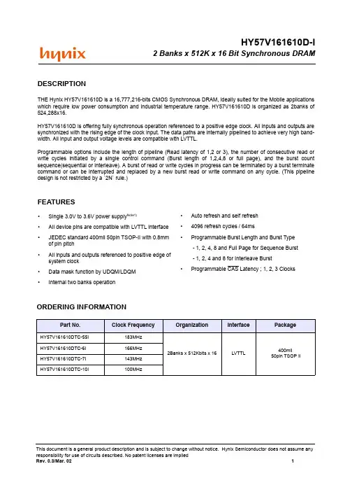
2 Banks x 512K x 16 Bit Synchronous DRAMThis document is a general product description and is subject to change without notice. Hynix Semiconductor does not assume any DESCRIPTIONTHE Hynix HY57V161610D is a 16,777,216-bits CMOS Synchronous DRAM, ideally suited for the Mobile applications which require low power consumption and industrial temperature range. HY57V161610D is organized as 2banks of 524,288x16.HY57V161610D is offering fully synchronous operation referenced to a positive edge clock. All inputs and outputs are synchronized with the rising edge of the clock input. The data paths are internally pipelined to achieve very high band-width. All input and output voltage levels are compatible with LVTTL.Programmable options include the length of pipeline (Read latency of 1,2 or 3), the number of consecutive read or write cycles initiated by a single control command (Burst length of 1,2,4,8 or full page), and the burst count sequence(sequential or interleave). A burst of read or write cycles in progress can be terminated by a burst terminate command or can be interrupted and replaced by a new burst read or write command on any cycle. (This pipeline design is not restricted by a `2N` rule.)FEATURES•Single 3.0V to 3.6V power supply Note1)•All device pins are compatible with LVTTL interface •JEDEC standard 400mil 50pin TSOP-II with 0.8mm of pin pitch•All inputs and outputs referenced to positive edge of system clock•Data mask function by UDQM/LDQM •Internal two banks operation•Auto refresh and self refresh •4096 refresh cycles / 64ms•Programmable Burst Length and Burst Type - 1, 2, 4, 8 and Full Page for Sequence Burst - 1, 2, 4 and 8 for Interleave Burst•Programmable CAS Latency ; 1, 2, 3 ClocksORDERING INFORMATIONPart No.Clock FrequencyOrganization Interface PackageHY57V161610DTC-55I 183MHz 2Banks x 512Kbits x 16LVTTL400mil 50pin TSOP IIHY57V161610DTC-6I 166MHzHY57V161610DTC-7I 143MHz HY57V161610DTC-10I100MHzPIN CONFIGURATIONPIN DESCRIPTIONPIN PIN NAME DESCRIPTIONCLK Clock The system clock input. All other inputs are referenced to the SDRAM on the rising edge of CLK.CKE Clock Enable Controls internal clock signal and when deactivated, the SDRAM will be one of the states among power down, suspend or self refresh.CS Chip Select Command input enable or mask except CLK, CKE and DQM BA Bank Address Select either one of banks during both RAS and CAS activity.A0 ~ A10Address Row Address : RA0 ~ RA10, Column Address : CA0 ~ CA7 Auto-precharge flag : A10RAS, CAS, WE Row Address Strobe,Column Address Strobe,Write EnableRAS, CAS and WE define the operation.Refer function truth table for detailsLDQM, UDQM Data Input/Output Mask DQM control output buffer in read mode and mask input data in write mode DQ0 ~ DQ15Data Input/Output Multiplexed data input / output pinV DD/V SS Power Supply/Ground Power supply for internal circuit and input bufferV DDQ/V SSQ Data Output Power/Ground Power supply for DQNC No Connection No connectionFUNCTIONAL BLOCK DIAGRAM 1Mx16 Synchronous DRAMABSOLUTE MAXIMUM RATINGSParameter Symbol Rating Unit Ambient Temperature T A- 40 ~ 85°CStorage Temperature T STG-55 ~ 125°CVoltage on Any Pin relative to V SS V IN, V OUT-1.0 ~ 4.6VVoltage on V DD relative to V SS V DD-1.0 ~ 4.6VShort Circuit Output Current I OS50mAPower Dissipation P D1WSoldering Temperature·Time T SOLDER260·10°C·SecNote : Operation at above absolute maximum rating can adversely affect device reliability.DC OPERATING CONDITION (TA= -40°C to 85°C)Parameter Symbol Min Typ.Max Unit Note Power Supply Voltage V DD, V DDQ 3.0 3.3 3.6V1, 2 Input high voltage V IH 2.0 3.0V DD + 0.3V1, 4 Input low voltage V IL-0.500.8V1, 5 Note :1.All voltages are referenced to V SS = 0V.2.V DD(min) is3.15V when HY57V161610DTC-7I operates at CAS latency=23.V IH(max) is acceptable4.6V AC pulse width with ≤ 10ns of duration.4.V IL(min) is acceptable -1.5V AC pulse width with ≤ 10ns of duration.AC OPERATING CONDITION (TA= - 40°C to 85°C, V DD=3.0V to3.6V, V SS=0V)Parameter Symbol Value Unit Note AC input high / low level voltage V IH / V IL 2.4/0.4VInput timing measurement reference level voltage Vtrip 1.4VInput rise / fall time tR / tF1nsOutput timing measurement reference level Voutref 1.4VOutput load capacitance for access time measurement CL30pF1 Note :1. Output load to measure access times is equivalent to two TTL gates and one capacitance(30pF).For details, refer to AC/DC output load circuit.2. V DD(min) is3.15V when HY57V161610DTC-7I operates at CAS latency=2 and tCK2=8.9nsCAPACITANCE (TA=25°C , f=1MHz)DC CHARACTERISTICS I (TA= - 40°C to 85°C )Note :1.V DD (min) is 3.15V when HY57V161610DTC-7I operates at CAS latency=2 and tCK2=8.9ns.2.V IN = 0 to3.6V, All other pins are not under test = 0V 3.D OUT is disabled, V OUT =0 to 3.6VParameterPinSymbol Min Max Unit Input capacitanceCLKC I1 2.54pF A0 ~ A10, BACKE, CS, RAS, CAS, WE, UDQM, LDQM C I2 2.55pF Data input / output capacitanceDQ0 ~ DQ15C I/O46.5pFParameterSymbolMin.Max Unit Note Power Supply Voltage V DD 3.0 3.6V 1Input leakage current IL -11uA 2Output leakage current IO -11uA 3Output high voltage V OH 2.4-V I OH = -4mA Output low voltageV OL-0.4VI OL =+4mADC CHARACTERISTICS II (TA= -40°C to 85°C , V DD =3.0V to 3.6V, V SS =0V Note1,2)Note :1.V DD (min) is 3.15V when HY57V161610DTC-7I operates at CAS latency=2 and tCK2=8.9ns.2.I DD1 and I DD4 depend on output loading and cycle rates. Specified values are measured with the output open.ParameterSymbolTest ConditionSpeedUnitNote-55I-6I-7I-10IOperating Current IDD1Burst Length=1, One bank active tRAS ≥ tRAS(min),tRP ≥ tRP(min), IO=0mA130120110110mAPrecharge Standby Currentin power down modeIDD2P CKE ≤ VIL(max), tCK = min.1mAIDD2PSCKE ≤ VIL(max), tCK = ∞1Precharge Standby Currentin non power down modeIDD2N CKE ≥ VIH(min), CS ≥ VIH(min), tCK = minInput signals are changed one time during 2Clks. All other pins ≥ VDD-0.2V or ≤ 0.2V20mAIDD2NS CKE ≥ VIH(min), tCK = ∞Input signals are stable.15Active Standby Current in power down modeIDD3P CKE ≤ VIL(max), tCK = min 3.0mAIDD3PSCKE ≤ VIL(max), tCK = ∞3.0Active Standby Current in non power down modeIDD3N CKE ≥ VIH(min), CS ≥ VIH(min), tCK = minInput signals are changed one time during 2CLKs. All other pins ≥ VDD-0.2V or ≤ 0.2V50mAIDD3NS CKE ≥ VIH(min), tCK = ∞Input signals are stable 30Burst Mode Operating CurrentIDD4tCK ≥ tCK(min),tRAS ≥ tRAS(min), IO=0mA All banks activeCL=313012011090mA2CL=2110110110-Auto Refresh Current IDD5tRRC ≥ tRRC(min), All banks active 130110110110mA Self Refresh CurrentIDD6CKE ≤ 0.2V2mAAC CHARACTERISTICS (TA= - 40°C to 85°C , V DD =3.0V to 3.6V, V SS =0V Note1,2)Note :1.V DD (min) is 3.15V when HY57V161610DTC-7I operates at CAS latency=2 and tCK2=8.9ns.2.tCK2 is 8.9ns only when tAC2 is 7.9ns in HY57V161610DTC-6I and HY57V161610DTC-7I.3.Assume tR / tF (input rise and fall time ) is 1ns.ParameterSymbol-55I-6I-7I-10IUnitNoteMinMaxMin MaxMin MaxMin MaxSystem clock cycle timeCL=3tCK3 5.56-7-10-nsCL=2tCK2-10-10-12-2Clock high pulse width tCHW 22- 2.5-3-ns 3Clock low pulse width tCLW 22- 2.5-3-ns3Access time from clock CL=3tAC35- 5.5-6-7nsCL=2tAC2-6-6-72Data-out hold time tOH 22- 2.5- 2.5-ns Data-Input setup time tDS 1.5 1.5- 1.75- 2.5-ns 3Data-Input hold time tDH 11-1-1-ns 3Address setup time tAS 1.5 1.5- 1.75- 2.5-ns 3Address hold time tAH 11-1-1-ns 3CKE setup time tCKS 1.5 1.5- 1.75- 2.5-ns 3CKE hold time tCKH 11-1-1-ns 3Command setup time tCS 1.5 1.5- 1.75- 2.5-ns 3Command hold time tCH 11-1-1-ns 3CLK to data output in low Z-timetOLZ22-2-2-nsCLK to data output in high Z-timetOHZ 2 5.52627310nsAC CHARACTERISTICS (TA= - 40°C to 85°C , V DD =3.0V to 3.6V, V SS =0V Note1,2))Note :1. V DD (min) is 3.15V when HY57V161610DTC-7I operates at CAS latency=2 and tCK2=8.9ns.2. A new command can be given tRRC after self refresh exit.ParamterSymbol-55I -6I -7I-10IUnitNoteMin MaxMin Max Min Max Min Max RAS cycle timeOperationtRC 5560-70-70-ns Auto RefreshtRRC 5560-70-80-ns RAS to CAS delay tRCD 16.518-20-20-ns RAS active time tRAS 38.5100K40100K 45100K 45100K ns RAS prechargetimetRP 33-3-2-CLK RAS to RAS bank active delay tRRD 22-2-2-CLK CAS to CAS bank active delay tCCD 11-1-1-CLK Write command to data-in delay tWTL 00-0-0-CLK Data-in to precharge command tDPL 11-1-1-CLK Data-in to active command tDAL 44-4-3-CLK DQM to data-in Hi-Z tDQZ 22-2-2-CLK DQM to data mask tDQM 00-0-0-CLK MRS to new command tMRD 22-2-2-CLK Precharge to data output Hi-Z tPROZ 33-3-3-CLK Power down exit time tPDE 11-1-1-CLK Self refresh exit time tSRE 11-1-1-CLK 2Refresh TimetREF6464-64-64msDEVICE OPERATING OPTION TABLEHY57V161610DTC-55ICAS Latency tRCD tRAS tRC tRP tAC tOH 183MHz3CLKs3CLKs7CLKs10CLKs3CLKs5ns2ns 166MHz3CLKs3CLKs7CLKs10CLKs3CLKs 5.5ns2nsHY57V161610DTC-6ICAS Latency tRCD tRAS tRC tRP tAC tOH 166MHz3CLKs3CLKs7CLKs10CLKs3CLKs 5.5ns2ns 143MHz3CLKs3CLKs7CLKs10CLKs3CLKs 5.5ns 2.5nsHY57V161610DTC-7ICAS Latency tRCD tRAS tRC tRP tAC tOH 143MHz3CLKs3CLKs7CLKs10CLKs3CLKs 5.5ns 2.5ns 100MHz2CLKs2CLKs5CLKs7CLKs2CLKs7ns 2.5nsHY57V161610DTC-10ICAS Latency tRCD tRAS tRC tRP tAC tOH 100MHz3CLKs2CLKs5CLKs7CLKs2CLKs7ns 2.5ns 83MHz2CLKs2CLKs4CLKs6CLKs2CLKs7ns 2.5nsCOMMAND TRUTH TABLENote :1. Exiting Self Refresh occurs by asynchronously bringing CKE from low to high.2. X=Do not care, L=Low, H=High, BA=Bank Address, RA= Row Address, CA=Column Address, Opcode=Operand Code, NOP=No Operation.CommandCKEn-1CKEn CS RAS CAS WE DQM A 0~A 9A10/AP BA NoteMode RegisterSet H X L L L L X OPcodeNo Operation H XHXXXXXLH H H Bank Active HXLLHHXRow AddressV ReadHXLHLHXColumn AddressL VRead with Auto precharge H WriteHXLHLLXColumn AddressLVWrite with Auto precharge H Precharge All BankHXLLHLXXHXPrecharge selected Bank L VBurst Stop H XLH HLX X U/LDQM H X V X Auto Refresh H H L L L H X XBurst-READ-Single-WRITEH X L L L L X A9 Pin High (Other Pins OP code)Self Refresh 1EntryH L L L L H XXExitLHHXXXXL H H H Precharge power downEntryHLHXXXXXL H H HExitLHHXXXXL H H H Clock SuspendEntryHLHXXXXXLVVVExitLHXXHY57V161610D-IRev. 0.3/Mar. 02 11PACKAGE INFORMATION400mil 50pin Thin Small Outline Package (TC)1Mx16 Synchronous DRAM UNIT : mm(inch)元器件交易网。
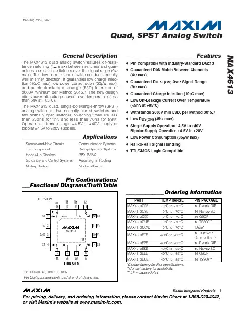
________________General DescriptionThe MAX4613 quad analog switch features on-resis-tance matching (4Ωmax) between switches and guar-antees on-resistance flatness over the signal range (9Ωmax). This low on-resistance switch conducts equally well in either direction. It guarantees low charge injec-tion (10pC max), low power consumption (35µW max),and an electrostatic discharge (ESD) tolerance of 2000V minimum per Method 3015.7. The new design offers lower off-leakage current over temperature (less than 5nA at +85°C).The MAX4613 quad, single-pole/single-throw (SPST)analog switch has two normally closed switches and two normally open switches. Switching times are less than 250ns for t ON and less than 70ns for t OFF .Operation is from a single +4.5V to +40V supply or bipolar ±4.5V to ±20V supplies.________________________ApplicationsSample-and-Hold Circuits Communication Systems Test Equipment Battery-Operated Systems Heads-Up DisplaysPBX, PABXGuidance and Control Systems Audio Signal Routing Military RadiosModems/Faxes____________________________Features♦Pin Compatible with Industry-Standard DG213♦Guaranteed R ON Match Between Channels (4Ωmax)♦Guaranteed R FLAT(ON)Over Signal Range (9Ωmax)♦Guaranteed Charge Injection (10pC max)♦Low Off-Leakage Current Over Temperature (<5nA at +85°C) ♦Withstands 2000V min ESD, per Method 3015.7♦Low R DS(ON)(85Ωmax)♦Single-Supply Operation +4.5V to +40V Bipolar-Supply Operation ±4.5V to ±20V ♦Low Power Consumption (35µW max)♦Rail-to-Rail Signal Handling ♦TTL/CMOS-Logic CompatibleMAX4613Quad, SPST Analog Switch________________________________________________________________Maxim Integrated Products 119-1362; Rev 3; 6/07________________Ordering InformationPin Configurations/___Functional Diagrams/TruthTable*Contact factory for dice specifications.**Contact factory for availability.***EP = Exposed PadFor pricing, delivery, and ordering information, please contact Maxim Direct at 1-888-629-4642,or visit Maxim’s website at .M A X 4613Quad, SPST Analog SwitchABSOLUTE MAXIMUM RATINGSELECTRICAL CHARACTERISTICS—Dual Supplies(V+ = 15V, V- = -15V, V L = 5V, GND = 0V, V INH = 2.4V, V INL = 0.8V, T A = T MIN to T MAX , unless otherwise noted.)Stresses beyond those listed under “Absolute Maximum Ratings” may cause permanent damage to the device. These are stress ratings only, and functional operation of the device at these or any other conditions beyond those indicated in the operational sections of the specifications is not implied. Exposure to absolute maximum rating conditions for extended periods may affect device reliability.Voltage Referenced to GNDV+......................................................................................+44V V-.........................................................................................-44V V+ to V-..............................................................................+44V V L ...................................................(GND - 0.3V) to (V+ + 0.3V)Digital Inputs V S_V D_ (Note 1)...................(V- - 2V) to (V+ + 2V)or 30mA (whichever occurs first)Continuous Current (any terminal)......................................30mA Peak Current, S_ or D_(pulsed at 1ms, 10% duty cycle max)...........................100mAContinuous Power Dissipation (T A = +70°C)Plastic DIP (derate 10.53mW/°C above +70°C).............842mW Narrow SO (derate 8.70mW/°C above +70°C).............696mW QSOP (derate 8.3mW/°C above +70°C).......................667mW Thin QFN (derate 33.3mW/°C above +70°C)..............2667mW TSSOP (derate 6.7mW/°C above +70°C).....................457mW Operating Temperature RangesMAX4613C_ _......................................................0°C to +70°C MAX4613E_ _...................................................-40°C to +85°C Storage Temperature Range.............................-65°C to +165°C Lead Temperature (soldering, 10sec).............................+300°CNote 1:Signals on S_, D_, or IN_ exceeding V+ or V- are clamped by internal diodes. Limit forward current to maximum current rating.MAX4613Quad, SPST Analog Switch_______________________________________________________________________________________3ELECTRICAL CHARACTERISTICS—Dual Supplies (continued)(V+ = 15V, V- = -15V, V L = 5V, GND = 0V, V INH = 2.4V, V INL = 0.8V, T A = T MIN to T MAX , unless otherwise noted.)ELECTRICAL CHARACTERISTICS—Single Supply(V+ = 12V, V- = 0V, V L = 5V, GND = 0V, V INH = 2.4V, V INL = 0.8V, T A = T MIN to T MAX , unless otherwise noted.)M A X 4613Quad, SPST Analog Switch 4_______________________________________________________________________________________ELECTRICAL CHARACTERISTICS—Single Supply (continued)(V+ = 12V, V- = 0, V L = 5V, GND = 0V, V INH = 2.4V, V INL = 0.8V, T A = T MIN to T MAX , unless otherwise noted.)Note 2:Typical values are for design aid only,are not guaranteed and are not subject to production testing. The algebraic convention,where the most negative value is a minimum and the most positive value a maximum, is used in this data sheet.Note 3:Guaranteed by design.Note 4:On-resistance match between channels and flatness are guaranteed only with bipolar-supply operation. Flatness is definedas the difference between the maximum and the minimum value of on-resistance as measured at the extremes of the speci-fied analog signal range.Note 5:Leakage parameters I S(OFF), I D(OFF), I D(ON), and I S(ON)are 100% tested at the maximum rated hot temperature and guaranteed at +25°C.Note 6:Off-Isolation Rejection Ratio = 20log (V D /V S ).Note 7:Between any two switches.__________________________________________Typical Operating Characteristics(T A = +25°C, unless otherwise noted.)O N L E A K A G E (n A )-2-112-15015V S , V D (V)-10-5510ON LEAKAGE CURRENTSO F F L E A K A G E (n A )-1-0.50.51V S , V D (V)-15015-10-5510OFF LEAKAGE CURRENTSV I N (V )0.51.52.02.53.03.5±5±10±15±20BIPOLAR SUPPLY VOLTAGE (V)SWITCHING THRESHOLD vs. BIPOLAR SUPPLY VOLTAGE02550751001255101520V D (V)R D S (O N ) (Ω)150ON-RESISTANCE vs. V D (UNIPOLAR SUPPLY VOLTAGE)R D S (O N ) (Ω)306090120-20-1001020V D (V)0ON-RESISTANCE vs. V D (BIPOLAR SUPPLY VOLTAGE)R D S (O N ) (Ω)020406080100V D (V)-15015-10-5510ON-RESISTANCE vs. V D (BIPOLAR SUPPLY VOLTAGE AND TEMPERATURE)MAX4613Quad, SPST Analog Switch_______________________________________________________________________________________5_____________________________Typical Operating Characteristics (continued)(T A = +25°C, unless otherwise noted.)255075100125150R D S (O N ) (Ω)4812V D (V)ON-RESISTANCE vs. V D (UNIPOLAR SUPPLY VOLTAGE AND TEMPERATURE)T I M E (n s )4080120160±5±10±15±20BIPOLAR SUPPLY VOLTAGE (V)SWITCHING TIME vs. BIPOLAR SUPPLY VOLTAGET I M E (n s )05010015020010152025UNIPOLAR SUPPLY VOLTAGE (V)SWITCHING TIME vs. UNIPOLAR SUPPLY VOLTAGEQ (p C )-200-102010-15-1001015V D (V)CHARGE INJECTION vs.V D VOLTAGEQ (p C )-105-551015V D (V)10CHARGE INJECTION vs.V D VOLTAGEM A X 4613Applications InformationGeneral Operation1)Switches are open when power is off.2)I N_, D_, and S_ should not exceed V+ or V-, even with the power off.3)Switch leakage is from each analog switch terminal to V+ or V-, not to other switch terminals.Operation with Supply VoltagesOther than ±15VUsing supply voltages less than ±15V will reduce the analog signal range. The MAX4613 operates with ±4.5V to ±20V bipolar supplies or with a +4.5V to +40V single supply; connect V- to GND when operating with a single supply. Also, all device types can operate with unbalanced supplies such as +24V and -5V. V L must be connected to +5V to be TTL compatible, or to V+ for CMOS-logic level inputs. The Typical Operating Characteristics graphs show typical on-resistance with ±20V, ±15V, ±10V, and ±5V supplies. (Switching times increase by a factor of two or more for operation at ±5V.)Overvoltage ProtectionProper power-supply sequencing is recommended for all CMOS devices. Do not exceed the absolute maximum ratings because stresses beyond the list-ed ratings may cause permanent damage to the devices. Always sequence V+ on first, followed byV L , V-, and logic inputs. If power-supply sequencing is not possible, add two small, external signal diodes in series with supply pins for overvoltage protection (Figure 1). Adding diodes reduces the analog signal range to 1V below V+ and 1V above V-, but low switch resistance and low leakage char-acteristics are unaffected. Device operation is unchanged, and the difference between V+ and V-should not exceed +44V.Quad, SPST Analog Switch 6_______________________________________________________________________________________Figure 1. Overvoltage Protection Using External Blocking DiodesMAX4613Quad, SPST Analog Switch_______________________________________________________________________________________7Figure 2. Switching TimeFigure 3. Break-Before-Make Test CircuitTiming Diagrams/Test Circuits____________________Revision HistoryPages changed at Rev 3: 1, 9, 10M A X 4613Quad, SPST Analog Switch 8________________________________________________________________________________________________________________________Timing Diagrams/Test Circuits (continued)Figure 5. Off-Isolation Rejection RatioFigure 6. CrosstalkFigure 7. Source/Drain-Off CapacitanceFigure 8. Source/Drain-On CapacitanceMAX4613Quad, SPST Analog Switch_______________________________________________________________________________________9Pin Configurations (continued)Package Information(The package drawing(s) in this data sheet may not reflect the most current specifications. For the latest package outline information go to /packages .)M A X 4613Quad, SPST Analog Switch Maxim cannot assume responsibility for use of any circuitry other than circuitry entirely embodied in a Maxim product. No circuit patent licenses are implied. Maxim reserves the right to change the circuitry and specifications without notice at any time.10____________________Maxim Integrated Products, 120 San Gabriel Drive, Sunnyvale, CA 94086 408-737-7600©2007 Maxim Integrated Productsis a registered trademark of Maxim Integrated Products.Package Information (continued)(The package drawing(s) in this data sheet may not reflect the most current specifications. For the latest package outline information go to /packages .)。
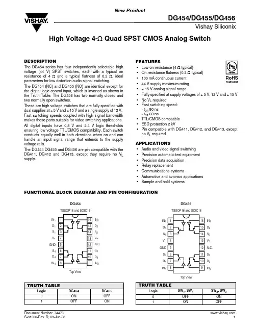
Vishay SiliconixDG454/DG455/DG456High Voltage 4-Ω Quad SPST CMOS Analog SwitchFEATURES•Low on-resistance (4 Ω typical)•On-resistance flatness (0.2 Ω typical) •100 mA continuous current •44 V supply maximum rating •± 15 V analog signal range•Fully specified at supply voltages of ± 5 V, 12 V and ± 15 V •NoV L required•Fast switching speed: - t on 80 ns - t off 60 ns•TTL/CMOS compatible •ESD protection 2 kV•Pin compatible with DG411, DG412, and DG413, exceptno V L requiredAPPLICATIONS•Audio and video signal switching •Precision automatic test equipment •Precision data acquisition •Relay replacement•Communications systems•Automotive and avionics applications •Sample and hold systemsDESCRIPTIONThe DG454 series has four independently selectable high voltage (44 V) SPST switches, each with a typical on resistance of 4 Ω and a typical flatness of 0.2 Ω, ideal parameters for low distortion audio signal switching.The DG454 (NC) and DG455 (NO) are identical except for the digital logic control input, which is inverted as shown in the Truth Table. The DG456 has two normally closed and two normally open switches.These are high voltage switches that are fully specified with dual supplies at ± 5 V and ± 15 V and a single supply of 12 V. Fast switching speeds coupled with high signal bandwidth makes these parts suitable for video switching applications.All digital inputs have 0.8 V and 2.4 V logic thresholds ensuring low voltage TTL/CMOS compatibility. Each switch conducts equally well in both directions when on and can handle an input signal range that extends to the supply voltage rails.The DG454 DG455 and DG456 are pin compatible with the DG411, DG412 and DG413, except they require no V L supply.FUNCTIONAL BLOCK DIAGRAM AND PIN CONFIGURATIONTRUTH TABLELogic DG454DG4550ON OFF 1OFFONTRUTH TABLELogic SW 1, SW 4SW 2, SW 30OFF ON 1ONOFFVishay SiliconixDG454/DG455/DG456Notes:a. - 40 °C to 85 °C datasheet limits apply.Notes:a. Signals on S X , D X , or IN X exceeding V+ or V- will be clamped by internal diodes. Limit forward diode current to maximum current ratings.b. All leads welded or soldered to PC board.c. Derate 5.6 mW/°C above 70 °C.d. Derate 8.0 mW/°C above 75 °C.ORDERING INFORMATIONTemp RangePackagePart NumberDG454/DG455/DG456- 40 °C to 125 °C a16-Pin TSSOPDG454EQ-T1-E3DG455EQ-T1-E3DG456EQ-T1-E316-Pin Narrow SOICDG454EY -T1-E3DG455EY -T1-E3DG456EY -T1-E3ABSOLUTE MAXIMUM RATINGS T A = 25 °C, unless otherwise notedParameter Limit Unit V+ to V- 44VGND to V- 25Digital Inputs a , VS , V D(V-) - 2 to (V+) + 2or 30 mA, whichever occurs firstContinuous Current (Any Terminal)100mA Peak Current, S or D (Pulsed 1 ms, 10 % Duty Cycle)300Storage T emperature - 65 to 150°C Power Dissipation (Package)b 16-Pin TSSOP c 450mW 16-Pin Narrow SOIC d 600Thermal Resistance (Package)b 16-Pin TSSOP 178°C/W 16-Pin Narrow SOIC125ESD (HBM)2kVSPECIFICATIONS FOR DUAL SUPPLIESParameter Symbol Test Conditions Unless Specified V+ = 15 V , V- = - 15 V V IN = 2.4 V , 0.8 V a Temp.b Typ.c- 40 to 125 °C- 40 to 85 °C UnitMin.dMax.dMin.dMax.dAnalog Switch Analog Signal Range e V ANALOG Full - 1515- 1515VOn-Resistance R ON I S = - 10 mA, V D = - 10 V to + 10 VRoom Full 3.8 5.38.3 5.37.3ΩOn-Resistance Match ΔR ONI S = - 10 mA, V D = ± 10 VRoom Full 0.120.510.50.5On-Resistance Flatness R FLATNESS I S = - 10 mA, V D = - 5 V , 0 V , + 5 V Room Full 0.250.50.50.50.5Switch OffLeakage Current I S(off)V D = ± 10 V , V S = 10 VRoom Full ± 0.1- 0.5- 200.520- 0.5- 2.50.52.5nA I D(off)Room Full ± 0.1- 0.5- 200.520- 0.5- 2.50.52.5Channel On Leakage CurrentI D(on)V S = V D = ± 10 VRoom Full± 0.1- 1- 40140- 1- 515±Vishay SiliconixDG454/DG455/DG456Parameter Symbol Test Conditions Unless Specified V+ = 15 V , V- = - 15 V V IN = 2.4 V , 0.8 V a Temp.b Typ.c- 40 to 125 °C- 40 to 85 °C UnitMin.dMax.dMin.dMax.dDigital Control Input Current, V IN Low I IL V IN Under T est = 0.8 V Full 0.005- 0.50.5- 0.50.5µA Input Current, V IN High I IH V IN Under T est = 2.4 VFull 0.005- 0.50.5- 0.50.5Input Capacitance e C INf = 1 MHzRoom7pFDynamic Characteristics T urn-On Time t ON R L = 300 Ω, C L = 35 pF V S = ± 10 V , See Figure 2Room Full 88118160118144nsT urn-Off Time t OFF Room Full 699712097112Break-Before-MakeTime Delay t D DG456 only, V S = 10 V R L = 300 Ω, C L = 35 pF Room 18Charge Injection e Q V g = 0 V , R g = 0 Ω, C L = 1 nFRoom 22pCOff Isolation eOIRR R L = 50 Ω, C L = 5 pFf = 1 MHzRoom - 60dB Channel-to-Channel Crosstalk eX TALK Room - 85Source Off Capacitance e C S(off) f = 1 MHzRoom 31pF Drain Off Capacitance e C D(off)Room 34Channel On Capacitance e C D(on)Room 103T otal Harmonic Distortion e THDSignal = 5 V RMS , 20 Hz to 20 kHz,R L = 600 ΩRoom0.04%Power Supplies Power Supply Current I+V+ = 16.5 V , V- = - 16.5 VV IN = 0 or 5 VRoom Full 25100100100100µANegative Supply Current I- Room Full - 0.001- 0.5- 5- 0.5- 5Ground CurrentI GNDRoom Full- 25- 100- 100- 100- 100SPECIFICATIONS FOR DUAL SUPPLIESSPECIFICATIONS FOR DUAL SUPPLIESParameter Symbol Test Conditions Unless Specified V+ = 5 V , V- = - 5 VV IN = 2.4 V , 0.8 V a Temp.b Typ.c- 40 to 125 °C - 40 to 85 °C UnitMin.dMax.dMin.dMax.dAnalog Switch Analog Signal Range e V ANALOG Full - 55- 55VOn-Resistance R ON V+ = + 5 V , V- = - 5 VI S = - 10 mA, V D = - 3.5 V to + 3.5 VRoom Full 3.811151112ΩOn-Resistance Match ΔR ONV+ = + 5 V, V- = - 5 V ,I S = - 10 mA, V D = ± 3.5 VRoom Full0.130.510.50.5Dynamic Characteristics T urn-On Time e t ON R L = 300 Ω, C L = 35 pF V S = 3 V, See Figure 2Room Full 170200296200256nsT urn-Off Time e t OFF Room Full 669612496113Break-Before-Make eTime Delay t D DG456 only, V S = 3 V R L = 300 Ω, C L = 35 pF Room 98Charge Injection eQV g = 0 V , R g = 0 Ω, C L = 1 nFRoom8pCVishay SiliconixDG454/DG455/DG456Notes:a. V IN = input voltage to perform proper function.b. Room = 25 °C, Full = as determined by the operating temperature suffix.c. Typical values are for DESIGN AID ONLY, not guaranteed nor subject to production testing.d. The algebraic convention whereby the most negative value is a minimum and the most positive a maximum, is used in this data sheet.e. Guaranteed by design, not subject to production test.Stresses beyond those listed under “Absolute Maximum Ratings” may cause permanent damage to the device. These are stress ratings only, and functional operation of the device at these or any other conditions beyond those indicated in the operational sections of the specifications is not implied. Exposure to absolute maximum rating conditions for extended periods may affect device reliability.Parameter Symbol Test Conditions Unless Specified V+ = 5 V , V- = - 5 VV IN = 2.4 V , 0.8 V a Temp.b Typ.c- 40 to 125 °C - 40 to 85 °C UnitMin.dMax.dMin.dMax.dPower Supplies Power Supply Current I+V IN = 0 or 5 VRoomFull 14100100100100µANegative Supply Current I- Room Full - 0.001- 0.5- 5- 0.5- 5Ground CurrentI GNDRoom Full- 14- 100- 100- 100- 100SPECIFICATIONS FOR DUAL SUPPLIESSPECIFICATIONS FOR UNIPOLAR SUPPLIESParameter Symbol Test Conditions Unless Specified V+ = 12 V, V- = 0 V V IN = 2.4 V, 0.8 V a Temp.b Typ.c- 40 to 125 °C- 40 to 85 °C UnitMin.dMax.dMin.dMax.dAnalog Switch Analog Signal Range e V ANALOG Full 1212VOn-Resistance R ON I S = - 10 mA, V D = 0 V to + 10 V Room Full 5.58.112.48.110.4ΩOn-Resistance Match ΔR ON I S = - 10 mA, V D = + 10 V Room Full 0.140.510.50.5On-Resistance Flatness R FLATNESSI S = - 10 mA, V D = 0 V , + 5 V , + 10 VRoom Full0.941.51.71.51.5Dynamic Characteristics Turn-On Time t ON R L = 300 Ω, C L = 35 pF V S = 8 V , See Figure 2Room Full 132162238162210nsTurn-Off Time t OFF Room Full 619111791105Break-Before-MakeTime Delay t D DG456 only, V S = 8 V R L = 300 Ω, C L = 35 pF Room 70Charge Injection e QV g = 0 V , R g = 0 Ω, C L = 1 nFRoom1pCPower Supplies Power Supply Current I+V+ = 13.5 V, V- = 0 VV IN = 0 or 5 VRoom Full 25100100100100µANegative Supply Current I- Room Full - 0.001- 0.5- 5- 0.5- 5Ground CurrentI GNDRoom Full- 25- 100- 100- 100- 100Vishay SiliconixDG454/DG455/DG456TYPICAL CHARACTERISTICS 25°C, unless otherwise notedDDOn-Resistance vs. V D and Single Supply VoltageDVishay SiliconixDG454/DG455/DG456TYPICAL CHARACTERISTICS 25°C, unless otherwise notedCharge Injection vs. Analog VoltageSwitching Time vs. Dual Supply VoltageSwitching Time vs. Single Supply VoltageSwitching Time vs. Temperature andDual Supply VoltageSingle Supply VoltageSupply Current vs. Input Switching FrequencyVishay SiliconixDG454/DG455/DG456TYPICAL CHARACTERISTICS 25°C, unless otherwise notedTEST CIRCUITSSwitching Threshold vs. Supply VoltageInsertion Loss, Off-Isolation, Crosstalkvs. FrequencyFigure 1. Switching TimeFigure 2. Break-Before-Make (DG456)Vishay SiliconixDG454/DG455/DG456TEST CIRCUITSVishay Siliconix maintains worldwide manufacturing capability. Products may be manufactured at one of several qualified locations. Reliability data for Silicon Technology and Package Reliability represent a composite of all qualified locations. For related documents such as package/tape drawings, part marking, and reliability data, see /ppg?74473.Figure 3. Charge InjectionFigure 4. CrosstalkFigure 5. Off-IsolationFigure 6. Source/Drain CapacitancesDisclaimer Legal Disclaimer NoticeVishayAll product specifications and data are subject to change without notice.Vishay Intertechnology, Inc., its affiliates, agents, and employees, and all persons acting on its or their behalf (collectively, “Vishay”), disclaim any and all liability for any errors, inaccuracies or incompleteness contained herein or in any other disclosure relating to any product.Vishay disclaims any and all liability arising out of the use or application of any product described herein or of any information provided herein to the maximum extent permitted by law. The product specifications do not expand or otherwise modify Vishay’s terms and conditions of purchase, including but not limited to the warranty expressed therein, which apply to these products.No license, express or implied, by estoppel or otherwise, to any intellectual property rights is granted by this document or by any conduct of Vishay.The products shown herein are not designed for use in medical, life-saving, or life-sustaining applications unless otherwise expressly indicated. Customers using or selling Vishay products not expressly indicated for use in such applications do so entirely at their own risk and agree to fully indemnify Vishay for any damages arising or resulting from such use or sale. Please contact authorized Vishay personnel to obtain written terms and conditions regarding products designed for such applications.Product names and markings noted herein may be trademarks of their respective owners.元器件交易网。
DW01A (文件编号:S&CIC0822)锂电池保护电路一、描述DW01A是一个锂电池保护电路,为避免锂电池因过充电、过放电、电流过大导致电池寿命缩短或电池被损坏而设计的。
它具有高精确度的电压检测与时间延迟电路。
二、主要特点工作电流低;过充检测4.3V,过充释放4.1V;过放检测2.4V,过放释放3.0V;过流检测0.15V,短路电流检测1.0V;充电器检测;过电流保护复位电阻;带自恢复功能工作电压范围广;小封装。
三、应用单一锂电池保护电路。
DW01A (文件编号:S&CIC0822)锂电池保护电路五、极限参数六、电气特性参数(除非特别指定,Tamb=25℃)过充电状态当从正常状态进入充电状态时,可以通过VDD检测到电池电压。
当电池电压进入到这充电状态时,VDD 电压大于VOC P,迟延时间超过TOC,M2关闭。
释放过充电状态进入过充电状态后,要解除过充电状态,进入正常状态,有两种方法。
●如果电池自我放电,并且VDD<VOCR,M2开启,返回到正常状态。
●在移去充电器,连接负载后,如果VDD<VOCP,M2开启,返回到正常模式。
过放电检测当由正常状态进入放电状态时,可以通过VDD检测到电池电压。
当电池电压进入过放电状态时,VDD电压小于VOD P,迟延时间超过TOD,则M1关闭。
释放过放电模式如果在过放电模式有一个充电器连接电池,电压将变为VCSI<VC HA和VDD>VODR,M1开启并返回到常模式;或者当负载悬空,VDD电压恢复到VDD>VODR,M1开启并返回到正常模式(自恢复功能)。
充电检测当一个充电器连接电池,电压将变为VCSI<VCHA,这样IC检测到充电器已接入。
过电流/短路电流检测在正常模式下,当放电电流太大时,由CSI管脚检测到电压大于VOIX(V OI1或V OI2),并且迟延大于TOIX(T OI1或T OI2),则代表过电流(短路)状态。
DG421/DG423/DG425Improved Low-Power,CMOS Analog Switches with Latches________________________________________________________________Maxim Integrated Products1_________________Pin Configurations__Functional Diagrams/Truth T ablesCall toll free 1-800-998-8800 for free samples or literature.19-0137; Rev 1; 3/94_______________General DescriptionMaxim’s redesigned DG421/DG423/DG425 monolithic analog switches now feature guaranteed on-resistance matching (3Ωmax) between switches and on-resistance flatness over the signal range (4Ωmax). These low on-resistance switches (20Ωtyp) conduct equally well in both directions. They guarantee a low charge injection of 15pC maximum and an ESD tolerance of 2000V minimum per Method 3015.7. Off leakage current over temperature has also been reduced (less than 5nA at +85°C).The DG421/DG423/DG425 are precision, dual CMOS switches with latchable logic inputs that simplify inter-facing with microprocessors (µPs). The single-pole/single-throw DG421 and double-pole/single-throw DG425 are normally open dual switches. The dual, single-pole/double-throw DG423 has two normally open and two normally closed switches. Fast switching times (175ns for t ON and 145ns for t OFF ) and low power consumption (35µW max) make these parts ideal for battery-powered applications requiring µP-compatible switches. Operation is from a single +10V to +30V supply,or bipolar ±4.5V to ±20V supplies. Fabricated with the same 44V silicon-gate process, these switches have rail-to-rail signal handling capabilities._______________________ApplicationsSample-and-Hold Circuits ModemsFax MachinesTest Equipment Battery-Operated SystemsPBX, PABX Guidance and Control Systems Military RadiosAudio Signal RoutingCommunication Systems______________________New Featureso Plug-In Upgrades for Industry-Standard DG421/DG423/DG425o Improved r (DS)ON Match Between Channels (3Ωmax)o Guaranteed r FLAT(ON)Over Signal Range (4Ωmax)o Improved Charge Injection (15pC max)o Improved Off Leakage Current Over Temperature (<5nA at +85°C)o Withstands Electrostatic Discharge (2000V min)per Method 3015.7__________________Existing Featureso Low r DS(ON)(35Ωmax)o Single-Supply Operation +10V to +30V Bipolar-Supply Operation ±4.5V to ±20V o Low Power Consumption (35µW max)o Rail-to-Rail Signal Handling Capability o TTL/CMOS-Logic Compatible______________Ordering Information*Contact factory for dice specifications.**Contact factory for availability and processing to MIL-STD-883B.D G 421/D G 423/D G 425Improved Low-Power,CMOS Analog Switches with LatchesVoltage Referenced to V-V+............................................................44V GND .........................................................25V V L ..................................(GND - 0.3V) to (V+ + 0.3V)Digital Inputs, V S , V D (Note 1)..............(V- - 2V) to (V+ + 2V)Current (any terminal, except S or D).................................30mA Continuous Current, S or D.................................................20mA Peak Current, S or D (pulsed at 1ms, 10% duty cycle max)...100mAContinuous Power Dissipation (T A = +70°C)16-Pin Plastic DIP (derate 10.53mW/°C above +70°C)...842mW 20-Pin PLCC (derate 10.00mW/°C above +70°C).....800mW 16-Pin CERDIP (derate 10.00mW/°C above +70°C) ...800mW Operating Temperature RangesDG42_C_..........................................0°C to +70°C DG42_D_ .......................................-40°C to +85°C DG42_A_ ......................................-55°C to +125°C Storage Temperature RangesDG42_C_/DG42_D_ ...........................-65°C to +125°C DG42_A_ .....................................-65°C to +150°C Lead Temperature (soldering, 10sec)....................+300°CELECTRICAL CHARACTERISTICS(V+ = 15V, V- = -15V, V L = +5V, GND = 0V, V INH = +2.4V, V INL = +0.8V, T A = T MIN to T MAX , unless otherwise noted.)Stresses beyond those listed under "Absolute Maximum Ratings " may cause permanent damage to the device. These are stress ratings only, and functional operation of the device at these or any other conditions beyond those indicated in the operational sections of the specifications is not implied. Exposure to absolute maximum rating conditions for extended periods may affect device reliability.ABSOLUTE MAXIMUM RATINGSNote 1:Signals on S, D, or IN exceeding V+ or V- are clamped by internal diodes. Limit forward current to maximum current ratings.DG421/DG423/DG425Improved Low-Power,CMOS Analog Switches with Latches_______________________________________________________________________________________3ELECTRICAL CHARACTERISTICS (continued)(V+ = 15V, V- = -15V, V L = +5V, GND = 0V, V= +2.4V, V = +0.8V, T = T to T , unless otherwise noted.)Note 2:Typical values are for design aid only , are not guaranteed, and are not subject to production testing. The algebraic convention,where the most negative value is a minimum and the most positive value a maximum, is used in this data sheet.Note 3:Guaranteed by design.Note 4:On-resistance match between channels and flatness are guaranteed only with bipolar-supply operation. Flatness is defined as the dif-ference between the maximum and minimum value of on-resistance as measured at the extremes of the specified analog signal range.Note 5:Leakage parameters I S(OFF), I D(OFF), and I D(ON)are 100% tested at the maximum rated hot temperature and guaranteed bycorrelation at +25°C.Note 6:Off-Isolation Rejection Ratio = 20log (V D /V S ), V D = output, V S = input to off switch.Note 7:Between any two switches.D G 421/D G 423/D G 425Improved Low-Power,CMOS Analog Switches with Latches 4_______________________________________________________________________________________505520-20ON-RESISTANCE vs. V D (DUAL-SUPPLIES)2545V D (V)r D S (O N ) (Ω)103530-100204015105355-20ON-RESISTANCE vs. V D AND TEMPERATURE (DUAL SUPPLIES)1030V D (V)r D S (O N ) (Ω)202015-101025014020ON-RESISTANCE vs. V D (SINGLE SUPPLY)40120V D (V)r D S (O N ) (Ω)208060515100107010ON-RESISTANCE vs. V D AND TEMPERATURE (SINGLE SUPPLY)2060V D (V)r D S (O N ) (Ω)20403051550101000.0001-75125OFF LEAKAGE CURRENTS vs.TEMPERATURE0.00110TEMPERATURE (°C)O F F L E A K A G E(n A )0.10.012511000.0001-75125ON LEAKAGE CURRENTS vs.TEMPERATURE0.00110TEMPERATURE (°C)O N L EA K A G E (n A )0.10.0125160-60-2020CHARGE INJECTION vs. ANALOG VOLTAGE-4040V D (V)Q(p C )100-20-100201000.0001-75125SUPPLY CURRENT vs. TEMPERATURE0.00110TEMPERATURE (°C)I +, I -, I L (µA )0.10.01251__________________________________________Typical Operating Characteristics(T A = +25°C, unless otherwise noted.)DG421/DG423/DG425Improved Low-Power,CMOS Analog Switches with Latches_______________________________________________________________________________________5___________________Pin Descriptions__________Applications InformationOperation with Supply VoltagesOther Than ±15VThe DG421/DG423/DG425 switches operate with ±4.5V to ±20V bipolar supplies or with a +10V to +30V single supply. In either case, analog signals ranging from V+to V- can be switched. The Typical Operating Characteristics graphs illustrate typical analog-signal and supply-voltage on-resistance variations. The usual on-resistance temperature coefficient is 0.5%/°C (typ).Logic InputsThese devices operate with a single positive supply or with bipolar supplies. They maintain TTL compatibility with supplies anywhere in the ±4.5V to ±20V range as long as V L = +5V. If V L is connected to V+ or another supply at voltages other than +5V, the devices will operate at CMOS-logic-level inputs.Overvoltage ProtectionProper power-supply sequencing is recommended for all CMOS devices. Do not exceed the absolute maxi-mum ratings because stresses beyond the listed rat-ings may cause permanent damage to the devices.Always sequence V+ on first, followed by V L , V-, and logic inputs. If power-supply sequencing is not possi-ble, add two small, external signal diodes in series with supply pins for overvoltage protection (Figure 1).Adding diodes reduces the analog signal range to 1V below V+ and 1V above V-, without affecting low switch resistance and low leakage characteristics. Device operation is unchanged, and the difference between V+and V- should not exceed +44V.D G 421/D G 423/D G 425Improved Low-Power,CMOS Analog Switches with Latches 6_______________________________________________________________________________________Figure 2. Switching TimeFigure 3. Latch TimingV OUT is the steady-state output with the switch on. Feedthrough via switch capacitance may result in spikes at the leading and trailing edge of the output waveform.______________________________________________Timing Diagrams/Test CircuitsDG421/DG423/DG425Improved Low-Power,CMOS Analog Switches with Latches_______________________________________________________________________________________7Figure 5. Charge Injection_________________________________Timing Diagrams/Test Circuits (continued)Figure 4. DG423 Break-Before-Make IntervalFigure 6 . Off-Isolation Rejection RatioD G 421/D G 423/D G 425Improved Low-Power,CMOS Analog Switches with Latches 8_______________________________________________________________________________________Figure 8. Drain/Source-Off Capacitance _________________________________Timing Diagrams/Test Circuits (continued)Figure 7. CrosstalkFigure 9. Drain/Source-On CapacitanceDG421/DG423/DG425Improved Low-Power,CMOS Analog Switches with Latches_____________________________________________Pin Configurations (continued)_____________________________Functional Diagrams/Truth Tables (continued)D G 421/D G 423/D G 425Improved Low-Power,CMOS Analog Switches with Latches 10______________________________________________________________________________________*Contact factory for dice specifications.**Contact factory for availability and processing to MIL-STD-883B._Ordering Information (continued)___________________________________________________________Chip Topographies(2.66mm)0.082" (2.08mm)D1S1IN1N.C.N.C.N.C.N.C.D2RS S2IN2V-VL V+WR(2.66mm)0.082" (2.08mm)D1S1IN1D3S3S4D4D2RSS2IN2V-VL V+WRDG421DG423DG421DG423/DG425V L V L TRANSISTOR COUNT: 100SUBSTRATE CONNECTED TO V+TRANSISTOR COUNT: 100SUBSTRATE CONNECTED TO V+DG421/DG423/DG425Improved Low-Power,CMOS Analog Switches with Latches______________________________________________________________________________________11________________________________________________________Package InformationMaxim cannot assume responsibility for use of any circuitry other than circuitry entirely embodied in a Maxim product. No circuit patent licenses are implied. Maxim reserves the right to change the circuitry and specifications without notice at any time.12__________________Maxim Integrated Products, 120 San Gabriel Drive, Sunnyvale, CA 94086 (408) 737-7600©1994 Maxim Integrated ProductsPrinted USAis a registered trademark of Maxim Integrated Products.D G 421/D G 423/D G 425Improved Low-Power,CMOS Analog Switches with Latches___________________________________________Package Information (continued)。
SymbolTyp Max 659085125R θJL 4380Maximum Junction-to-Lead CSteady-State°C/WThermal Characteristics ParameterUnits Maximum Junction-to-Ambient AF t ≤ 10s R θJA °C/W Maximum Junction-to-Ambient A Steady-State °C/W AO3401AAO3401ASymbolMin TypMaxUnits BV DSS -30V -1T J =55°C-5I GSS ±100nA V GS(th)-0.6-1-1.3V I D(ON)-25A 3644T J =125°C52634455m Ω6280m Ωg FS 13S V SD -0.75-1V I S-2A C iss 9331200pF C oss 108pF C rss 81pF R g69ΩQ g 9.312.2nC Q gs 1.5nC Q gd 3.7nC t D(on) 5.2ns t r 6.8ns t D(off)42ns t f 15ns t rr 2128ns Q rr14.3nCTHIS PRODUCT HAS BEEN DESIGNED AND QUALIFIED FOR THE CONSUMER MARKET. APPLICATIONS OR USES AS CRITICAL COMPONENTS IN LIFE SUPPORT DEVICES OR SYSTEMS ARE NOT AUTHORIZED. AOS DOES NOT ASSUME ANY LIABILITY ARISING OUT OF SUCH APPLICATIONS OR USES OF ITS PRODUCTS. AOS RESERVES THE RIGHT TO IMPROVE PRODUCT DESIGN,FUNCTIONS AND RELIABILITY WITHOUT NOTICE.Body Diode Reverse Recovery TimeBody Diode Reverse Recovery Charge I F =-4.3A, dI/dt=100A/µsDrain-Source Breakdown Voltage On state drain currentI D =-250µA, V GS =0V V GS =-2.5V, I D =-2.5AV GS =-4.5V, V DS =-5V V GS =-10V, I D =-4.3AReverse Transfer Capacitance Electrical Characteristics (T J =25°C unless otherwise noted)STATIC PARAMETERS ParameterConditions I DSS µA Gate Threshold Voltage V DS =V GS I D =-250µA V DS =-30V, V GS =0VV DS =0V, V GS =±12V Zero Gate Voltage Drain Current Gate-Body leakage current R DS(ON)Static Drain-Source On-ResistanceForward TransconductanceDiode Forward Voltage m ΩV GS =-4.5V, I D =-3.5A I S =-1A,V GS =0V V DS =-5V, I D =-4.3AI F =-4.3A, dI/dt=100A/µsV GS =0V, V DS =-15V, f=1MHz SWITCHING PARAMETERS Total Gate Charge V GS =-4.5V, V DS =-15V, I D =-4.3AGate Source Charge Gate Drain Charge Turn-On Rise Time Turn-Off DelayTime V GS =-10V, V DS =-15V, R L =3.5Ω, R GEN =6ΩGate resistanceV GS =0V, V DS =0V, f=1MHzTurn-Off Fall TimeMaximum Body-Diode Continuous CurrentInput Capacitance Output Capacitance Turn-On DelayTime DYNAMIC PARAMETERS A: The value of R θJA is measured with the device mounted on 1in 2 FR-4 board with 2oz. Copper, in a still air environment with T A =25°C. The value in any given application depends on the user's specific board design. B: Repetitive rating, pulse width limited by junction temperature.C. The R θJA is the sum of the thermal impedence from junction to lead R θJL and lead to ambient.D. The static characteristics in Figures 1 to 6 are obtained using <300 µs pulses, duty cycle 0.5% max.E. These tests are performed with the device mounted on 1 in 2 FR-4 board with 2oz. Copper, in a still air environment with T A =25°C. The SOA curve provides a single pulse rating.F.The current rating is based on the t ≤ 10s thermal resistance rating.Rev0: Apr.2007AO3401AAO3401A。
40#:西门子S7-200中文软件资料包(1CD 共650M)包含:西门子新版LOGOV4.0控制器编程软件,LOGO新版使用手册大全。
新版S7-200PLC 中文版编程软件,s7_200_sim中文版模拟软件,S7-200的中文系统手册大全。
S7-200上位机软件PC_Access_V10。
OP、TP系列中文版编程软件及编程手册大全,WINCC中文版编程手册,Protool中文手册,西门子STEP5教程中文版(NEW),PG702编程器操作手册,所有西门子公司自动化设备相关的中文资料,S7-200与S7-300的应用论文集,S7-200的应用实例(中文注释),S7-400.S7-300梯形图(LAD) 中文版编程手册等。
(共650M,详细清单见40#盘说明)最新资料请浏览:欢迎光临本站!最新软件资料清单请发邮件索取:mailto:plc808@ QQ:121667231西门子软件目录:1 ADDON-CPU·226可支持新的CPU226XM.2 LOGO!3.1!编程软件套装软件3 LOGO!编程软件套装软件4 LOGO2.0!编程软件套装软件V3.2新版的编程软件5 MicroWin6 Microwin3.0x_chinese 汉化3.0(X)版7 Microwin3.11的升级版,只有此版软件才支持Toolbox8 microwin311_chinese汉化3.1版9 Microwin311_SP2_chinese 汉化3.1版10 Microwin311编程软件STEP7-Micro.win 32 Version3.111 PLCSIM_V50西门子PLCSIM_V5012 s7_200_sim模拟软件汉化版13 s7_200_sim模拟运行软件14 S7_200模拟软件1.215 SIMOVIS控制和调试软件16 STEP7-200V3.01新版的编程软件17 toolbox包括Uss指令和Tp070的组态软件Tp Designer v1.018 TP 7 Version 2.30组态软件19 tp7c的组态软件20 西门子S7-200套装软件21 新版的编程软件STEP7-Micro.win 32 Version3.1西门子资料目录:1 组态软件ProTool操作指南中文版2 注塑机专用变频器资料中文版3 中央空调节能控制系统(中文)4 有几个WinCC数据库编程的资料1、2、35 一个初学PLC系统的教程1、2、36 一个pid编程实例的pdf文件中文版7 现代可编程序控制器原理与应用S7-300-上册8 现代可编程序控制器原理与应用S7-300-下册9 现场总线的应用!(中文)10 现场总线的协议介绍!(中文)11 西门子专用变频器Eco 操作手册12 西门子通用变频器应用实例手册中文版13 西门子通用变频器西兴平化肥厂的应用14 西门子风机类专用变频器使用手册中文版15 西门子变频器MM 430操作手册中文版16 西门子STEP5教程中文版(NEW)17 西门子S7-400硬件安装手册中文版18 西门子S7-300模块手册中文版19 西门子PLC模块型号&功能大全.files20 西门子PLC模块型号与功能查询大全21 人机介面Td200的中文手册22 绕线机程序例子 123 强化地板生产企业,浸渍线调胶IFA系统程序24 模拟量转换的程序说明的pdf文件25 模拟量转换的程序说明(中文)26 触摸面板Tp170_c操作面板OP170-B设备手册27 WINCC中文版(所有WINCC中文资料)28 wincc2(组态)(中文版第二册)29 wincc1(组态)(中文版第一册)30 VS710SIMATIC VS710视觉系统使用手册中文版31 TP27和TP37应用软件使用手册中文版32 STEP7 系列培训课程--硬件组态33 STEP7 系列培训课程--常用功能块编程使用手册34 STEP7 网络组态步骤教程中文版.doc35 Software_Protection授权手册中文版36 sitop开关电源使用手册37 SITOP开关电源订货数据38 SIMATIC-NET网络解决方案中文版39 SIMATIC.HMI-WINCC手册(第一册)中文版40 SIMATIC S5的通讯管理中文版41 SIEMENS新一代过程控制系统 PCS 742 SIEMENS技术支持与服务手册43 SIEMENS变频手册中文版44 SETP7- V5.0使用入门中文版45 s7硬件和网络课程教程中文版46 S7功能模块说明_2(中文)47 S7功能模块说明_1(中文)48s7-400.S7-300语句表编程中文版(NEW)49S7-400.S7-300梯形图编程手册(中文)50 S7-400 CPU及模板规范参考手册51 s7-300可编程控制器CPU314C-2DP技术参数52 S7-300_S7-400指令列表中文版53 s7-300 M7-300 模板规范参考手册中文版54 S7-2MW3K指令说明55 S7-200与S7-300的应用论文集中文版56 S7-200选型样本中文版57 S7-200的中文系统手册2(编程手册第二册))58 S7-200的中文系统手册1(编程手册第一册))59 S7-200的应用实例(中文注释)60 S7-200的应用实例(程序)61 s7-200mw3k帮助指令中文版62 s7-200与TD200连接说明63 S7-200CPU215与CPU315的PROFIBUSDP连接手册64 S7-200 应用示例中文版65 s7-200 tip&tricks_chinese 应用示例中文版66 S7-200 Manual Chinese编程手册67 pulsator 通用变频器驱动装置-在化工企业搅拌机上的应用68 Protool组态图形显示中文手册69 PROTOOL-Runtime用户指南中文版70 PROTOOL-PRO使用入门中文版71 ProTool_基于Windows的用户手册中文版72 PROTOOL 基于WINDOWS的系统用户手册中文版73 PROFIBUS技术标准中文版74 PROFIBUS概论中文版75 Profibus_接口部件使用手册中文版76 PROFIBUS 现场总线技术问题77 Profibus Ethernet S7通讯。