CS6718_MYSON代理
- 格式:pdf
- 大小:202.40 KB
- 文档页数:15

SONiX公司保留對以下所有產品在可靠性、功能和設計方面的改進做進一步說明的權利。
SONiX不承擔由本手冊所涉及的產品或電路的運用和使用所引起的任何責任。
SONiX的產品不是專門設計應用於外科植入、生命維持和任何SONiX產品的故障會對個體造成傷害甚至死亡的領域。
如果將SONiX的產品應用於上述領域,即使這些是由SONiX在產品設計和製造上的疏忽引起的,用戶也應賠償所有費用、損失、合理的人身傷害或死亡所直接或間接產生的律師費用,並且用戶保證SONiX及其雇員、子公司、分支機搆和銷售商與上述事宜無關。
V1.0 2007年3月第一版目錄修改記錄 (2)1MP-III WRITER介紹 (4)1.1簡介 (4)1.2功能概述 (4)1.3硬體介紹 (4)1.4配件說明 (5)1.5軟硬體安裝 (6)1.5.1軟體安裝 (6)1.5.2硬體安裝 (6)2晶片脫機燒錄操作 (8)2.1晶片脫機燒錄步驟 (8)2.2下載燒錄代碼 (8)2.3晶片脫機燒錄 (8)3晶片聯機燒錄操作 (9)3.1晶片聯機燒錄步驟 (9)3.2R OLLING CODE設定 (14)EEPROM操作 (15)4MP-III WRITER脫機操作說明 (17)4.1MP-III W RITER 脫機操作的功能表及相關資訊說明 (17)4.2MP-III W RITER 操作說明 (17)5常見故障排除 (19)5.1進入T EST M ODE (19)5.2常見故障維修方法 (19)6附錄 (20)1 MP-III Writer介紹1.1 簡介MP-III Writer是基於MPI Writer升級的新一代燒錄器,擴展有USB介面和ISP(In System Program)等功能,可通過USB口下載燒錄代碼,更新燒錄控制程式。
由硬體升級改為軟體升級,極大方便了客戶的使用。
1.2 功能概述採用具有ISP功能的Flash Base MCU,聯機狀態時根據需要可升級晶片燒錄控制程式;Full Speed USB1.1介面可方便與PC互聯,從而進行燒錄器升級、聯機燒錄晶片或下載晶片燒錄代碼; 支援晶片聯機和脫機燒錄操作;繼承MPI Writer所有功能;新增聯機狀態下,讀取晶片資料的功能;新增聯機狀態下,讀取EEPROM和清空EEPROM等功能。

ErrataTitle & Document Type:Manual Part Number:Revision Date:HP References in this ManualThis manual may contain references to HP or Hewlett-Packard. Please note that Hewlett-Packard's former test and measurement, semiconductor products an d chemical analysisbusinesses are now part of Agilent Technologies. We have made no changes to thismanual copy. The HP XXXX referred to in this document is now the Agilent XXXX.For example, model number HP8648A is now model number Agilent 8648A.About this ManualWe’ve added this manual to the Agilent website in an effort to help you support yourproduct. This manual provides the best information we could find. It may be incomplete or contain dated information, and the scan quality may not be ideal. If we find a bettercopy in the future, we will add it to the Agilent website.Support for Your ProductAgilent no longer sells or supports this product. You will find any other availableproduct information on the Agilent Test & Measurement website:Search for the model number of this product, and the resulting product page will guideyou to any available information. Our service centers may be able to perform calibrationif no repair parts are needed, but no other support from Agilent is available.3562A Programming Manual03562-90031October 1985Artisan Technology Group - Quality Instrumentation ... Guaranteed | (888) 88-SOURCE | Artisan Technology Group - Quality Instrumentation ... Guaranteed | (888) 88-SOURCE | Artisan Technology Group - Quality Instrumentation ... Guaranteed | (888) 88-SOURCE | Artisan Technology Group - Quality Instrumentation ... Guaranteed | (888) 88-SOURCE | Artisan Technology Group - Quality Instrumentation ... Guaranteed | (888) 88-SOURCE | Artisan Technology Group - Quality Instrumentation ... Guaranteed | (888) 88-SOURCE | Artisan Technology Group - Quality Instrumentation ... Guaranteed | (888) 88-SOURCE | Artisan Technology Group - Quality Instrumentation ... Guaranteed | (888) 88-SOURCE | Artisan Technology Group - Quality Instrumentation ... Guaranteed | (888) 88-SOURCE | 。

Agilent 81689A / 81689B / 81649A Compact Tunable Laser Modules Technical SpecificationsFebruary 2002The 81689A, 81689B, 81649A compact tunable lasermodules offer superior performance now also in the compactmodule class. As they are tunable with continuous outputpower, they are the most flexible stimulus for the test ofoptical amplifiers, DWDM components as well as for the testof complete DWDM systems.Compact tunable lasers for C-and L-bandThe Agilent 81689A and 81689B modules operate in the C-band from 1525 nm to 1575 nm, whereas the Agilent 81649A covers the L-band from 1570 nm to 1620 nm.Test of optical amplifiersA variable amount of the compact, yet fully remote controlled Agilent 81689A, 81689B and 81649A tunable laser modules, in combination with the 81682A and 81642A high power Tunable Laser, is the ideal solution to characterize optical amplifiers for use in DWDM applications. The 81689A, 81689B and 81649A compact tunable laser modules provide the high stimulus power needed to test today's optical amplifiers. Together with the 81651A optical attenuator module, an output power dynamic range of more than60 dB can be achieved. Even without the attenuator module the power can be attenuated by 9dB (10dB for 81689B) e.g. to equalize power levels of several sources. Polarization Maintaining Fiber for the test of integrated optical devicesThe 81689A, 81689B and 81649A modules are ideally constructed to characterize integrated optical devices. Their optional Panda PMF output ports provide a well defined state of polarization to ensure constant measurement conditions on waveguidedevices. A PMF cable easily connectsan external optical modulator.The 81689A, 81689B and 81649A isavailable with both, standard single-mode fiber and Panda type PMF.Compact module for DWDMmulti-channel testThe 81689A, 81689B and 81489Aallow a realistic multi-channel test bedfor DWDM transmission systems to beset up.Their flexibility make them thepreferred choice for tests of DWDMtransmission system during installationand maintenance phases.Compact spare for DFBmodules in ITU gridsThe 81689B for the first time solvesthe sparing nightmare for users ofDWDM combs. In combination with acomb of 81662A DFB lasers the81689B can replace any DFB between1525nm and 1575nm without powerpenalty.Remote control & PnPsoftware drivers for easyprocess automationIts continuous, mode-hop free tuningmakes it quick and easy to set even themost complex configurations to thetarget wavelengths and power levels,just by dialing or using the vernier keys.A 8163B mainframe can host2 compact tunable laser modules. Thisallows for the most compact C- and L-band stimulus solution available today.Each 8164B mainframe can host up tofour units of the 81689A, 81689B or81649A in its upper slots.The 8166B is most interesting for highchannel count solutions. Up to17 compact tunable laser modules canbe hosted here.The 81649A, 81689A and 81689B areproduced to ISO 9001 internationalquality system standard as part ofAgilent's commitment to continuallyincreasing customer satisfactionthrough improved quality control.Specifications describe theinstrument's warranted performance.They are verified at the end of a 2 mlong patchcord and are valid afterwarm-up and for the stated outputpower and wavelength ranges.Each specification is assured bythoroughly analyzing all measurementuncertainties. Supplementaryperformance characteristics describethe instrument’s non-warranted typicalperformance.Every instrument is delivered with acommercial certificate of calibrationand a detailed test report.For further details on specifications,see the Definition of Terms in AppendixC of the Compact Tunable Laser User'sGuide.81689A, 81689B, 81649A Compact Tunable Laser for Multi-channel test applicationsAgilent 81689A Agilent 81689B Agilent 81649A Wavelength range1525 nm to 1575 nm1525 nm to 1575 nm1570 nm to 1620 nm Wavelength resolution0.01 nm, 1.25 GHz at 1550 nm0.01 nm, 1.25 GHz at 1550 nm0.01 nm, 1.17 GHz at 1595 nm Absolute wavelength accuracy (typ.) [1]±0.3 nm±0.3 nm±0.3 nmRelative wavelength accuracy [1]±0.3 nm±0.15 nm±0.15 nmWavelength repeatability [1]±0.05 nm±0.05 nm±0.05 nmWavelength stability(typ., over 24 h at constant temperature)[1] (typ., over 1 h at constant temperature)[1]±0.02 nm±0.01 nm±0.005 nm±0.01 nm±0.005 nmTuning speed (typ.)<10 sec/ 50 nm<10 sec/ 50 nm<10 sec/ 50 nmLinewidth (typ.) [2]with Coherence Control ON (typ.) [2]20 MHz---< 20MHz>100MHz< 20MHz>100MHzOutput power (continuous power on duringtuning)≥ 6 dBm (1525 –1575nm)≥ 10 dBm (1525 –1575nm)≥ 6 dBm (1570 –1620nm) Minimum output power–3 dBm0 dBm–3 dBmPower stability (at constant temperature) [3]±0.03 dB over 1 hour,typ. ±0.06 dB over 24 hours ±0.015 dB over 1 hour,typ. ±0.0075 dB over 1 hour,typ. ±0.05 dB over 24 hours±0.015 dB over 1 hour,typ. ±0.0075 dB over 1 hour,typ. ±0.05 dB over 24 hoursPower repeatability (typ.) [3]±0.02 dB±0.02 dB±0.02 dB Power linearity±0.1dB±0.1dB±0.1dB Power flatness versus wavelength±0.3 dB±0.2 dB±0.2 dBSide-mode suppression ratio (typ.) [2]> 40 dB(1525 – 1575 nm at 0 dBm)> 45 dB(1525 – 1575 nm at ≥ 3 dBm)> 45 dB(1570 – 1620 nm at ≥ 0 dBm)Signal to source spontaneous emission ratio (typ.) [4]≥ 39 dB/ nm(1525 –1575 nm at 6 dBm)≥ 44 dB/ nm(1525 –1575 nm at 10 dBm)≥ 42 dB/ nm(1570 – 1620 nm at 6 dBm)Relative intensity noise (RIN, typ.)< -137 dB/Hz(100 MHz – 2.5 GHz, at +3 dBm)< -137 dB/Hz(100 MHz – 2.5 GHz, at +7 dBm)< -137 dB/Hz(100 MHz – 2.5 GHz, at +3 dBm)Dimensions75 mm H, 32 mm W, 335 mm D(2.8" x 1.3" x 13.2")75 mm H, 32 mm W, 335 mm D(2.8" x 1.3" x 13.2")75 mm H, 32 mm W, 335 mm D(2.8" x 1.3" x 13.2")Weight 1 kg 1 kg 1 kg[1]At CW operation. Measured with wavelength meter based on wavelength in vacuum.[2]Measured by heterodyning method.[3]500 ms after changing power.[4]Measured with optical spectrum analyzer at 1 nm resolution bandwidth.Listed optionsOption 021: standard single mode fiber,straight contact output connectorOption 022: standard single mode fiber,angled contact output connectorOption 071: polarization maintainingfiber, straight contact output connectorOption 072: polarization maintainingfiber, angled contact output connectorSupplementary performance characteristics ModulationInternal digital modulation50% duty cycle, 200 Hz to 300 kHz.>45% duty cycle, 300 kHz to 1 MHz. Modulation output (via Mainframe): TTL reference signal.External digital modulation> 45% duty cycle, fall time< 300 ns, 200 Hz to 1 MHz. Modulation input (via Mainframe):TTL signal.External analog modulation≥ ±15% modulation depth,5 kHz to 1 MHz.Modulation input: 5 Vp-p Coherence control(81649A/81689B)For measurements on components with 2 m long patchcords and connectors with 14 dB return loss, the effective linewidth results in a typical power stability of< ±0.025 dB over1 minute by reducing interference effects in the test setup.GeneralOutput isolation (typ.):38 dBReturn loss (typ.):55 dB (options 022, 072)40 dB (options 021, 071)Polarization maintaining fiber (Options071, 072)Fiber type: Panda.Orientation: TE mode in slow axis,in line with connector key.Extinction ratio: 16 dB typ.Laser class:Class IIIb according to FDA 21 CFR1040.10, Class 3A according to IEC 825- 1; 1993.Recommended re-calibration period:2 years.Warm-up time:< 40 min,immediate operation after boot-up.EnvironmentalStorage temperature:–20 °C to +70 °C (81689A)–40 °C to +70 °C (81689B, 81649A)Operating temperature:15 °C to 35 °CHumidity:< 80 % R.H. at 15 °C to 35 °CSpecifications are valid in non-condensingconditions.Laser Safety InformationAll laser sources specified by this datasheet are classified as Class 1Maccording to IEC 60825-1 (2001).All laser sources comply with 21 CFR1040.10 except for deviations pursuantto Laser Notice No. 50, dated 2001-July-26This page intentially left blankAgilent Technologies’Test and Measurement Support,Services, and AssistanceAgilent Technologies aims to maximize the value you receive, while minimizing your risk and problems. We strive to ensure that you get the test and measurement capabilities you paid for and obtain the support you need. Our extensive support resources and services can help you choose the right Agilent products for your applications and apply them successfully. Every instrument and system we sell has a global warranty. Support is available for at least five years beyond the production life of the product. Two concepts underlie Agilent's overall support policy: "Our Promise" and "Your Advantage."Our PromiseOur Promise means your Agilent test and measurement equipment will meet its advertised performance and functionality. When you are choosing new equipment, we will help you with product information, including realistic performance specifications and practical recommendations from experienced test engineers. When you use Agilent equipment, we can verify that it works properly, help with product operation, and provide basic measurement assistance for the use of specified capabilities, at no extra cost upon request. Many self-help tools are available.Your AdvantageYour Advantage means that Agilent offers a wide range of additional expert test and measurement services, which you can purchase according to your unique technical and business needs. Solve problems efficiently and gain a competitive edge by contracting with us for calibration, extra-cost upgrades, out-of-warranty repairs, and on-site education and training, as well as design, system integration, project management, and other professional engineering services. Experienced Agilent engineers and technicians worldwide can help you maximize your productivity, optimize the return on investment of your Agilent instruments and systems, and obtain dependable measurement accuracy for the life of those products.By internet, phone, or fax, get assistance with all your test & measurement needsOnline assistance:Related Agilent Literature:/coms/lightwaveAgilent 8163A Lightwave MultimeterPhone or Fax Agilent 8164A Lightwave Measurement SystemUnited States:Agilent 8166A Lightwave Multichannel System(tel)180****4844Technical Specificationsp/n 5988-1568ENCanada:(tel)187****4414Agilent 81662A DFB Laser(fax) (905) 206 4120Agilent 81663A DFB LaserAgilent Fabry Perot LaserTechnical SpecificationsEurope:p/n 5988-1570EN(tel) (31 20) 547 2323(fax) (31 20) 547 2390Agilent Power Sensor ModulesJapan:Agilent Optical Heads(tel) (81) 426 56 7832Agilent Return Loss Modules(fax) (81) 426 56 7840Technical Specificationsp/n 5988-1569ENLatin America:(tel) (305) 269 7500(fax) (305) 269 7599Agilent 8163A/B Lightwave MultimeterAgilent 8164A/B Lightwave Measurement SystemAustralia:Agilent 8166A/B Lightwave Multichannel System(tel) 1 800 629 485 Configuration Guide(fax) (61 3) 9210 5947p/n 5988-1571ENNew Zealand:Agilent 8163B Lightwave Multimeter(tel) 0 800 738 378Agilent 8164B Lightwave Measurement System(fax) 64 4 495 8950Agilent 8166B Lightwave Multichannel SystemTechnical SpecificationsAsia Pacific:p/n 5988-3924EN(tel) (852) 3197 7777(fax) (852) 2506 9284Product specifications and descriptions in this document subject to change without notice.Copyright © 2001 Agilent TechnologiesFebruary 12 20025988-3675EN。

RUDAT-6000-30Key FeaturesProgrammable AttenuatorUSB / RS232Case Style: MS1813Software PackageThe Big Deal• Attenuation range, 30 dB• Fine attenuation resolution, 0.25 dB• Short attenuation transition time (650 ns)• Compact size, 2.0 x 3.0 x 0.6”• USB and RS232 control50Ω 0 – 30 dB, 0.25 dB step 1 to 6000 MHzProduct OverviewMini-Circuits’ RUDAT-6000-30 is a general purpose, single channel programmable attenuator suitable for a wide range of signal level control applications from 1 MHz to 6 GHz. The Attenuator provides 0 to 30 dB attenuation in 0.25 dB steps. Its unique design maintains linear attenuation change per dB, even at the highest attenuation settings.The attenuator is housed in a compact and rugged package with SMA female connectors on the bi-directional input and output RF ports, a standard 9 pin D-Sub and a USB type Mini-B power and control ports.The attenuator can be controlled via USB or RS232 (via D-Sub connector). Full software support is provided and can be downloaded from our website any time at /softwaredownload/patt.html . The package includes our user-friendly GUI application for Windows ® and a full API with programming instructions for Windows ® and Linux ® environments (both 32-bit and 64-bit systems).Trademarks: Windows is a registered trademark of Microsoft Corporation in the United States and other countries. Linux is a registered trademark of Linus Tor-valds. Mac is a registered trademark of Apple Corporation. Pentium is a registered trademark of Intel Corporation. Neither Mini-Circuits nor the Mini-Circuits RUDAT-series attenuators are affiliated with or endorsed by the owners of the above referenced trademarks.Mini-Circuits and the Mini-Circuits logo are registered trademarks of Scientific Components Corporation.Rev. KECO-008003EDR-10982/5Applications• Automated Test Equipment (ATE)• WiMAX, 3G, 4G, LTE, DVB Fading Simulators • Laboratory Instrumentation • Handover system Evaluation • Power level cyclingIncluded AccessoriesModel No.DescriptionQty.MUSB-CBL-3+2.6 ft. USB cable11 Attenuator RF ports are interchangeable, and support simultaneous, bidirectional signal transmission, however the specifications are guaranteed forthe RF in and RF out as noted on the label. There may be minor changes in performance when injecting signals to the RF Out port. 2 Max accuracy defined as ±[absolute error+% of attenuation setting] for example when setting the attenuator to 18 dB attenuation the maximum error will be: ±(0.95+0.02x18)= ±(0.95+0.36)= ± 1.31 dB.3 Total operating input power from both RF In and RF Out out ports. Compression level not noted as it exceeds max safe operating power level.4 Isolation is defined as max attenuation plus insertion loss; this is the path loss through the attenuator when initially powered up. After a brief delay (~0.5 sec typically) the attenuator will revert to a user defined “power-up” state (either max attenuation or a pre-set value).5 Tested with 1 MHz span between signals.6 Minimum Dwell Time is the time the RUDAT will take to respond to a command to change attenuation states without communication delays. In PC control add communication delays (on the order of msec for USB) to get actual response time.7Attenuation Transition Time is specified as the time between starting to change the attenuation state and settling on the requested attenuation state.8 Supply voltage +5V at Pin#1 of D-sub connector applies to units with S/N 11405010010 and greater.9 Power on sequence for RS232 control: Connect 5V power followed by the control lines.Absolute Maximum RatingsPermanent damage may occur if any of these limits are exceeded. Operation in the range between the max operating power and the absolute maximum rating for extended periods of time may result in reduced life and reliability.Operating Temperature 0°C to 50°C Storage Temperature-20°C to 85°C Voltage input at RS232 receive pin -30V to +30V Voltage input at RS232 transmit pin 0V to +4V Voltage input at RS232 Pin#1-1V to +6VV USB Max.6V DC voltage at RF port16V Total RF power for RF In & RF Out @ 1 to 10 MHz +13 dBm @ 10 to 6000 MHz+23 dBm10 Block diagram and connection shown apply to units with S/N 11405010010 and greater, for units with lowerS/N see archive section on page 9.11 Pin#1 can be used as supply voltage (+) pin instead of USB connection. When USB power is connected,Pin#1 may be connected to GND or supply voltage (+) or remain disconnected.12 Power on sequence for RS232 control: Connect 5V power followed by the control lines.Block Diagram 10USBSimultaneous, bidirectional RF signal transmission with symmetrical performanceNot ConnectedRS232Transmit (2)Receive (3)NC (4)GND (5)(6)(7)(8)(9)Supply voltage (1)*9 Pin D-SubPin Connections 10PIN NumberFunction2Transmit 3Receive 5GND 1+5 V DC 11,124,6-9Not ConnectedConnectionsRF IN (SMA female)RF OUT (SMA female)USB (USB type Mini-B female)RS232*(9 Pin D-Sub female)The 5V DC the D-Sub port.inch2X SMA FEMALEBracket OptionQTop ViewBottom View4X #2-56 UNCInstruction for mounting bracket:1. Tool required: Phillips head screwdriver2. Mount the bracket over threaded holes on the bottom side with the fasteners provided with the bracket.Attenuation Accuracy @ +25°Cvs. Frequency over Attenuation settings-1.0-0.50.00.51.01.50100020003000400050006000Frequency (MHz)A c c u r a c y(d B)Attenuation Accuracy @ 0°Cvs. Frequency over Attenuation settingsFrequency (MHz)A c c u r a c y (dB )Attenuation Accuracy @ +50°Cvs. Frequency over Attenuation settingsFrequency (MHz)A c c u r a c y (d B )Attenuation relative to I.L @ +25°C vs. Frequency over Attenuation settings0.010.020.030.040.00100020003000400050006000Frequency (MHz)Attenuation relative to I.L @ 0°C vs. Frequency over Attenuation settingsFrequency (MHz)A t t e n u a t i o n (dB )Attenuation relative to I.L @ +50°C vs. Frequency over Attenuation settings Frequency (MHz)A t t e n u a t i o n (dB )A t t e n u a t i o n (dB )1 1000 2000 3000 4000 5000 60001 1000 2000 3000 4000 5000 6000Attenuation relative to Insertion Loss @ +25°C vs. Frequency over Attenuation settings Attenuation relative to Insertion Loss @ 0°C vs. Frequency over Attenuation settings Attenuation relative to Insertion Loss @ +50°C vs. Frequency over Attenuation settingsInput VSWR @ +25°Cvs. Frequency over Attenuation settings1.01.21.41.61.82.00.001000.002000.003000.004000.005000.006000.00Frequency (MHz)I n p u t V S W R (:1)Ouput VSWR @ +25°Cvs. Frequency over Attenuation settings1.01.21.41.61.82.00.001000.002000.003000.004000.005000.006000.00Frequency (MHz)O u t p u t V S W R (:1)Insertion Loss @ Input Power=0dBm 0123450100020003000400050006000Frequency (MHz)I n s e r t i o n L o s s (d B )Insertion Loss @ Input Power +20 dBmvs. Frequency over Temperatures Insertion Loss @ Input Power=+23dBm123450100020003000400050006000Frequency (MHz)I n s e r t i o n L o s s (d B )Insertion Loss @ Input Power 0dBm vs. Frequency over Temperatures11000 2000 3000 4000 5000 6000 101000 2000 3000 4000 5000 6000 1 1000 2000 3000 4000 50006000 1 1000 2000 3000 4000 5000 6000Output VSWR @ +25°C vs. Frequency over Attenuation settings Input VSWR @ +25°C vs. Frequency over Attenuation settings IP3 @ 0dB AttenuationFrequency (MHz)I P 3 (d B m )Input IP3 @ 0dB Attenuationvs. Frequency over Temperatures Attenuation Setting (dB)A t t e n u a t i o n A c c u r a c y (dB )• Mini-Circuits’ full software and support package including user guide, Windows GUI, DLL files, programming manual and examples can be downloaded free of charge from /softwaredownload/patt.html • Please contact ****************************** for supportGraphical User Interface (GUI) for Windows Key Features:• Manual attenuation setting• Sweep and Hop attenuation sequences directed from the PC, or entire sequence loaded into RUDAT.• Attenuator address configuration and Firmware upgrade • Attenuation at power up may be set to selected attenuation level or last attenuation state recorded.• USB or RS232 control of RUDATApplication Programming Interface (API)Windows Support:• API DLL files exposing the full switch functionality See programming manual at https:///softwaredownload/Prog_Manual-6-Programmable_Attenuator.pdf for details • ActiveX COM DLL file for creation of 32-bit programs • .Net library DLL file for creation of 32 / 64-bit programs• Supported by most common programming environments (refer to application note AN-49-001 for summary of tested environments)Linux Support:• Full switch control in a Linux environment is achieved by way of USB interrupt commands. See programming manual at https:///softwaredownload/Prog_Manual-6-Programmable_Attenuator.pdf for detailsModelDescriptionRUDAT-6000-30USB/RS232 Programmable AttenuatorAdditional NotesA. Performance and quality attributes and conditions not expressly stated in this specification document are intended to be excluded and do not form a part of this specification document.B. Electrical specifications and performance data contained in this specification document are based on Mini-Circuit’s applicable established test performance criteria and measurement instructions.C. The parts covered by this specification document are subject to Mini-Circuits standard limited warranty and terms and conditions (collectively, “Standard Terms”); Purchasers of this part are entitled to the rights and benefits contained therein. For a full statement of the Standard Terms and the exclusive rights and remedies thereunder, please visit Mini-Circuits’ website at /MCLStore/terms.jspIncluded Accessories Part No.DescriptionMUSB-CBL-3+2.6 ft (0.8 m) USB Cable: USB type A(Male) to USB typeMini-B(Male)Optional AccessoriesDescriptionUSB-AC/DC-5 13,14AC/DC 5V DC Power Adapter with US, EU, IL, UK, AUS, and China power plugsMUSB-CBL-3+ (spare) 2.6 ft (0.8 m) USB Cable: USB type A(Male) to USB type Mini-B(Male)MUSB-CBL-7+ 6.6 ft (2.0 m) USB Cable: USB type A(Male) to USB type Mini-B(Male)D-SUB9-MF-6+ 6 ft RS232 Cable: 9 pin D-sub(Male) to 9 pin D-sub(Female)BKT-3901+Bracket kit including 3.75” x 2.00” bracket, mounting screws and washers13 Not used in USB control. USB-AC/DC-5 can be used to provide the 5VDC power when control is via RS232; units with S/N11405010010 and greater can also accept DC supply voltage at Pin#1 of the D-sub connector.14 Power plugs for other countries are also available, Plugs for other countries are also available, if you need a power plug for a country not listed please contact ******************************Block DiagramUSBSimultaneous, bidirectional RF signal transmission with symmetrical performanceNot ConnectedRS232Transmit (2)Receive (3)NC (4)GND (5)(6)(7)(8)(9)NC (1)ConnectionsRF IN (SMA female)RF OUT (SMA female)USB (USB type Mini-B female)RS232*(9 Pin D-Sub female)*9 Pin D-SubPin Connections 16Pin NumberFunction2Transmit 3Receive 5GND 1,4,6-9Not Connected16 Supply voltage can be provided via USB port only. When using RS232 control, powermust be provided to the USB port via either USB-AC/DC-5 power adaptor or a USB bus.。

服务热线:400-150-1816电话*************传真*************地址:北京市昌平区创新路27号昌平科技园区3号5层网址:北京威林视讯科技有限公司VLINC专业视听显控产品手册专业音视频产品与解决方案提供商2022北京威林视讯科技有限公司COMPANY PROFILE公司简介威林的愿景威林的使命威林的核心价值观威林视讯是专注于显示控制一体化解决方案的科技企业,经过多年发展,已经成长为国内显控领域的知名品牌,拥有多项独立自主的知识产权。
自成立以来,威林视讯连续推出多个创新产品,包括纯硬件图像处理器,到图像综合管理平台,从分布式处理器到可视化分布式系统,从46寸液晶拼墙到70寸液晶拼墙,从高清到8K 系统整体解决方案,威林视讯的每一次创新都引导着行业的发展和进步,威林视讯提出的所见即所得,所得即可操作的理念,已经成为显控系统的行业标准。
威林视讯有拥有强大的研发实力和方案设计服务能力,核心团队均具备10年以上的行业经验,与北京大学,北京交通大学等多所高校建立产学研合作关系,在掌握图像算法,具备产品设计能力的基础上,对于客户的订制化需求能够快速响应,从研发到制造,从设计到施工,建立了一整套的客户服务体系。
威林视讯在北京,上海,深圳,广州,南京,成都,南昌,乌鲁木齐等国内主要城市均设有分支机构,具备国内省会级城市的快速响应能力。
威林视讯的团队成功完成多个典型案例,包括北京新机场,北京公安局合成作战指挥中心,天津市委宣传部,国家气象局,火箭军某基地,上海联通,广州移动,酒泉卫星发射基地,滴滴出行等标志性项目,均为所在领域的标杆项目。
共同成长作为一个发展中的公司,威林愿意帮助客户成长,努力给客户提供技术培训,商务支持等各种支持,希望客户在竞争中取胜,威林的体系对客户保持开放,愿意帮助客户建立认证体系和获得各种知识产权。
同样,威林也希望能够跟员工一起成长,公司鼓励员工参加各种学历或者非学历教育并承担部分学费,公司内部也会不断建设良好的分享,培训和晋升的体系,希望能够鼓励每一位员工都能发挥自己最大的价值。
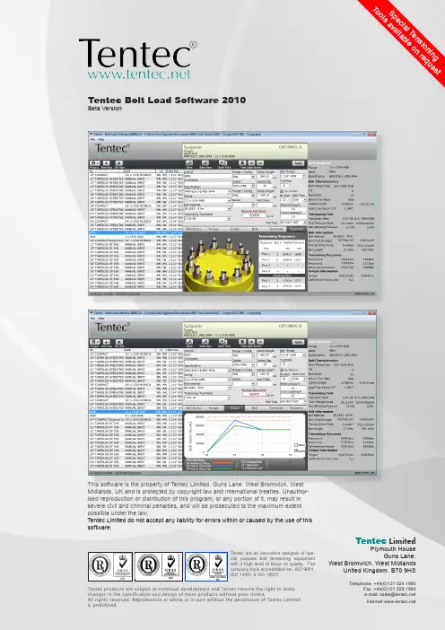
• Instruction Manual - Tentec Bolt Load Software a lTvaiTentec are an innovative designer of spe-cial purpose bolt tensioning equipmentwith a high level of focus on quality. Thecompany have accreditation to:- ISO 9001,ISO 14001 & ISO 18001Tentec LimitedPlymouth HouseGuns Lane.West Bromwich. West MidlandsUnited Kingdom. B70 9HS Tentec Bolt Load Software 2010Beta VersionThis software is the property of Tentec Limited. Guns Lane. West Bromwich. WestMidlands. UK and is protected by copyright law and international treaties. Unauthor-ised reproduction or distribution of this program, or any portion of it, may result insevere civil and criminal penalties, and will be prosecuted to the maximum extentpossible under the law.Tentec Limited do not accept any liability for errors within or caused by the use of thissoftware.Contents.Page 3 Introduction.Page 4 Project List, Header Window.Page 5 Tool BarsPage 6 Application definition, Joint Inspector.Page 7 Information Tab Bar, Setting up a projectPage 8 Project Definition Window.Page 9 Setting up the application.Page 12 Information Tabs.Page 14 Manual Input Mode, File MenuPage 15 File MenusPage 16 Summary Report.Page 17 Individual Application Report.Minimum System RequirementsOperating system: Windows XP with Service Pack 2 (32-bit edition only), Windows Vista (32-bit or 64-bit editions), Windows 7 Beta (32-bit or 64-bit editions), or Windows Server 2008.Processor: 1 GHz or higher for Windows Vista; 800 MHz or higher for Windows XP Memory: 128 MB of RAM (256 MB or more recommended) for Windows XP; 512 MB for Windows VistaResolution: Minimum 1024 x 768Notes:Tentec Bolt Load Software is currently in beta.It contains data for the Subsea Optimus 6, Optimus 5 & Topside CTST Range of Tentec Bolt Tensioning Tools.It is possible to replace the Tentec Logo on the documentation that the software produces in order to brand the documentation to another company.It is not possible to brand the software to another companyWe would hope that our partners that use the beta version of the software help us by making suggestions and reporting any problems they encounter with the software.It has been developed completely in-house by Tentec and as such we have the ability to implement changes and add features.Due to its beta status the software will fail to work at the end of each month and will require the latest version to be downloaded and installed, this is to ensure our partners are using the latest version.There is currently no input of flange material, it is assumed that adequate strength flange materials are being used. Stainless Steel 316 flanges are not to be tensioned with the recommended bolt stresses.The following flange materials or equivalents are suitable for the recommended bolt stresses.ASTM A105ASTM A182 Grades F65ASTM A182 Grade F60ASTM A182 Grade F52ASTM A182 Grade F50ASTM A182 Grade F51ASTM A350 Grade LF2ASTM A350 Grade LF3ASTM A694 Grade F52ASTM A694 Grade F60ASTM A694 Grade F65Standard ANSI B16.5 Flanges manufactured from material with yield strength equal to or greater than 247N/mm2 (35840lbs/In2)ANSI B16.5 Flange specification does not implicitly specify a minimum target bolt stress. The software will suggest recommend-ed target bolt stress values for these flanges. The recommended values are based on the experience of Tentec Limited and are used without any guarantee or liability to Tentec Limited. The recommended bolt stress values assume that flange material yield strength is equal to or greater than 247N/mm2 (35840lbs/In2).DO NOT USE THE RECOMMENDED ANSI B16.5 BOLT STRESS VALUES FOR FLANGES MANUFACTURED WITH MATE-RIAL YIELD STRENGTH LESS THAN 247N/mm2 (35840lbs/In2)The data produced by this software is only applicable when using Tentec Bolt Tensioning tools.Flange Service Temperature range for the recommended bolt stress values are -101ºc to +200ºc. Or as limited by the piping class specifications or the the bolt minimum or maximum temperature specification. Do not use the recommended bolt stress values outside of this range of temperature.Paul EggintonEngineering DirectorTentec LimitedAugust 2009The Tentec Bolt Load Software is a purpose designed software package, that allows rapid creation of nec-essary documentation for topside and subsea bolt tensioning projects. The package was designed with the philosophy of minimal input, maximum output. Documentation for multiple bolted joint projects can be created very quickly with minimal operator input. The software package contains data for the following standard bolted flanges.ANSI B16.5 MSS-SP44Norsok L-005 issue2IntroductionThe Main ScreenProject ListHeader ScreenThis area gives details of the current selected applications and the global project header information. This area also displays the current selected Tentec tool range.Application Tool BarThis area is the main control tool bar.Project - Global project header information can be set upAdd App - A new blank application can be created.Del App - Applications from the Project List can be deletedSave-Overwrites the currently selected application in the Project list with the currentinformation shown in the application definition areaSave New - Saves a new application entry in the Project List area with the current information in the application definition area.Save PDF’s - Generates a summary document and a multi-page application docu-ment. (PDF Format)View PDFs - Allows the user to view the summary and application documentsApply- Used to update the data in the application definition areaProject Tool BarThis area is above the project list.Project - Global project header information can be set upAdd App - A new blank application can be created.Del App - Applications from the Project List can be deletedJoint InspectorThis area is where the current bolted joint application is displayed.information Tab BarThis area is where catagorised information for the current application is displayed. The are 6 tabs.Bolt StressTorqueLoad GraphBoltToolSequenceSetting up a Project.Selecting the Projects button in the Tool Bar opens up the project definition windowProject Definition WindowHere the user sets up the global project information, which appears on the application documentationCustomerProject NameReference NoDateEngineerNotesSummary Documentation NotesTool Range - Select the relevant range of Tentec tools to use on all applications in the project.Only a single range of tools per project can be selected. It is not possible to change the selected range of tools to use once a project contains an application.Tool Ranges Available• Optimus 5 Subsea Tool Range• Optimus 6 Subsea Tool Range• CTST Topside RangeCross Loading %Here you can set the % factor that defines the global difference between the first and second pass tool pressures when using a 50% or 25% tool to bolt ratio. (It is possible to define a different factor on each application by altering the cross loading %in the application definition areaDefault = 20%Detensioning %Here you can set the % factor that defines the global detensioning pressure. The detensioning pressure is set at the residual bolt load value and a + or - % will set up a deviation from the residual bolt load base value.Torque Coefficient Friction FactorDefines the global friction value to be used on all torque load conversions.(It is possible to define a different friction factor on each application by altering the friction factor in the Information Tab Bar select Torque Tab)Default = 0.12Stress areas are based on:-Defines if the bolt stress is calculated using the Bolt Tensile Stress Area or Bolt MinorDiameter Area. ( The software defaults to Tensile Stress Area)ABCDEFG HJL MKISetting up your first applicationA A free form cell that allows the user to give a unique name to the bolted jointB Defines the flange specification (note the use of the manual input mode is detailedlater in this document, this part of the document only refers to the choice of ANSIFlanges, API Flanges or Norsok Flanges)C Defines the flange rating.D Defines the bolt material for the applicationE Selects the appropriate Tentec tool for the applicationF Allows the user to apply a comment to the application that appears on the individualapplication documentsG Defines the configuration of the flange 1 configuration and enters the thickness ofthe flange at HIn the case of a special thickness flange being used the flange thickness can be edited.J Defines the configuration of the flange 2 configuration and enters the thickness of theflange at KIn the case of a special thickness flange being used the flange thickness can be edited.I Defines the Gasket gap between the 2 mating flanges. This value can be edited.Flange 1Flange 1Flange 2Flange 2Clamp Length 1Clamp Length 2Clamp Length 1select “BlindThread” & enterthe length of en-gaged thread.Note: For a special Blind Threaded hole flange selectBlind Thread in Flange -2 config & enter the value of theengaged thread length into the clamp length 2 field.L In some cases an application may be fitted with washers below the joints application hexagon nuts. Enter the washer thickness here MIt is possible to define a single washer, 2 washers or a single spacer.Selecting “Auto Spacer” from the Spacer drop down menu, allows the software to calculate a suitable spacer thick-ness based on a target Load Transfer Factor (Note the lowest LTF when using bolt tensioning tools is 1.15). The software will not allow a target load transfer factor that is greater than the current LTF.N This cell defines the suitable Bolt diameter for the selected flange. It defaults to anInch imperial thread but can be changed to a metric bolt thread.P This cell defines if a maximum detensioning pressure is detailed on the applicationdocuments. (Refer to the note at the bottom of the summary document regarding the use of max detensioning pressures.)The maximum detensioning pressure defaults to a value equal to the 2nd pass toolpressure B. This can be edited on a global basis in the project definition window. To edit the detensioning pressure, per application, apply a plus or a negative % deviation value to cell U 0% gives a detensioning pressure = Pressure B, first pass pressure.O This cell defines either the pitch (metric threads) or the Threads per Inch - TPI (impe-rial threads) The defaults are:-Imperial threads - 8UN threads except UNC threads below 1” diameter MetricThreads - ISO Course pitch series.It is possible to edit the Pitch/TPI value if the applications calls for different thread forms.N O P QR U WSTQ Defines the number of bolts on the selected flangeS Recommended Reaction Nut Type. The software recommends the type of reaction nut to use and is depenedent on the flange bolt loading requirements. This cell only ap-pears if the selected tool range is Optimus 6.T Residual Bolt Stress, here is where the software recommends the residual boltstress, it can be overwritten by clicking on the cell which opens up a edit windowallow you to save the application to the project if the tool working pressures exceed the maximum working pressure of the tool, in this instance it will offer you a choice of either down rating the target bolt stress to a level within the capacity of the selected tool or to adjust the application parameters.Be aware that if you down rate the recommended residual bolt stress the application will not be tensioned in accordance with API or Norsok specifications. ANSI Flanges do not specify recommended residual bolt stresses.Bolt load can be defined in terms of either.. Target Residual Bolt Stress (psi) (lbs/In2) Target Residual Bolt Stress (N/mm2). Residual % of Bolt Yield (%) Residual Bolt Load (Tons)The edit window allows the user to overwrite the recommended bolt load or bolt stress in a variety of formats. Once the default recommended bolt stress is edited a yellow exclamation icon appears next to the value and the value is italicized. Clicking on the icon restores the default recommended bolt stressInformation Tab BarThe information tab bar consists of 6 Tabs labeled Bolt Stress Torque Load Graph Bolt ToolSequenceBolt Stress TabDisplays Bolt Stress, Bolt Load and % Bolt Yield over a 3 stage time period.Warning indicators will appear if the % bolt yield ex-ceeds 95% of bolt yield. It is Tentec policy not to exceed 95% of the bolt yield strength.This tab also allows the user to switch between using bolt tensile stress area and bolt minor area to calculate bolt stress. When switching a new bolt load is calculated based on the type of bolt area chosen.This tab displays the torque value to achieve the re-sidual bolt load based on the displayed coefficients of friction. The global coefficient of friction value can be edited in the project definition window. Changing the coefficient value in the Torque Tab only changes it for the current application.Torque TabStress Graph TabThis tab displays the predicted bolt stress path overa 3 point time period.T0 = Unstressed boltT1 = Initial bolt stress A pressureT1 = Initial bolt stress B pressureT2 = Final residual bolt stressThe Red line indicates the yield strength of the boltThe yellow line indicates the maximum detension-ing stress.Units can be switched between Metric and Imperial. Bolt TabThis tab displays the bolt detailNo edit is available from this TabThe Bolt Length value is based on the Tentec toolrange chosen in the Project Definition Window. Tool TabThis tab displays the recommended Tensioning ToolNo edit is available from this TabThe Bolt Length value is based on the Tentec toolrange chosen in the project definition window.When a special tensioner is chosen, this tab will bedisabled.Sequence TabThis tab displays the recommended tensioningsequence.Manual Input ModeAll 6 orange fields in the application definition area are to be completed first before the Joint Inspector displays the results. It is recommended that the bolt thread is selected first. Once the thread is selected the software will suggest tensioning tools in the tensioning tool ident menu.The tensioning tool ident menu will display all tools available for the selected bolt size, these include the standard tools from the particular Tentec tool range selected plus any user defined tensioning tools. A user defined tool can be defined by selecting “Spe-cial tool library” from the File/Special Tools Library menu.In manual input mode the software will not recommend a residual bolt stress .Here special tools can be added to your library of tools. Once defined the tool will be available from the Tension-ing Tool Ident cell for selection in manual mode whenever the library click the add button and enter the required the list and select the edit button open up, enter the special tool details. Click OK to leave the special tools library.project file. The name is built from the following vari-ables from the project definition window.Reference: in this case 4064 R1Note R1 represents “Revision1” can be used as a simple revision counter.Project: Pig Launcher Pulling HeadsThe summation of the two viariables makes the project file name.Note:Similar file names are created for the report PDF Files.File MenuThis logo can be changed in order to“Badge” the documentation to anothercompanyTo change the image copy a 220 x 110pxbitmap file to the software installation folder, thefile should be named logo.bmpSummary ReportBolt Load% of Bolt YieldProposed Tensioning ToolKey to GraphT0=Unloaded Bolt T1=Tensioner Initial Load T2= Tensioner Residual Load (retained)Flange Configuration WN WNPredicted Bolt Stress PathPass 11--Pass 2Pass 3Pass 4Pass 11--Pass 11--Checking Pass Pass psi bar Tensioner Bolt #Applied Pressure© 2009 Tentec Limited - All Rights Reserved This Logo can be changed in order to “Badge” the documentation to another companyTo change the image copy a 220 x 110pxbitmap file to the software installation folder, the Individual Application ReportTentec LimitedPlymouth HouseGuns LaneWest Bromwich. West MidlandsUnited Kingdom. B70 9HSTentec products are subject to continual development and Tentec reserve the right to。

I-7188EXC Language Based Embedded ControllerQuick Start GuideProduct Website:/i_7188ex_512.htmlIntroductionThe I-7188EX is powered by 80188-40 processor with 512K bytes of static RAM, and 512K bytes of Flash memory. One serial RS-232 port and one RS-485 port are provided. Ethernet support is provided by a NE-2000 compatible controller with 16K bytes of on-chip buffer memory and 10Base-T media interface. The I-7188EX also provides 14 user defined I/O lines. A cost-effective I/O expansion board with A/D, D/A, relay drivers and protected inputs is available. The I-7188EX also supports battery back-up SRAM disk board and Flash-Rom board, providing non-volatile mass storage from 2 megabytes to 64 megabytes. The 10BASE-T port is equipped with a RJ-45 connector. The 10BASE-T interface supports max 100-meter Cable length between I-7188EX and the network hub. This Guide offers information to guide youStep 1 ~ Step 4 - Start-up your deviceStep 5 ~ Step 7 - Configure device’s Ethernet settingsStep 8 ~ Step 11 - Download program to your device.I-7188EX C Language Based Embedded Controller- QuickStart (Feb/2016)I-7188EX C Language Based Embedded Controller- QuickStart (Feb/2016)/vxcomm.htmlI-7188EX C Language Based Embedded Controller- QuickStart (Feb/2016)I-7188EX C Language Based Embedded Controller- QuickStart (Feb/2016)I-7188EX C Language Based Embedded Controller- QuickStart (Feb/2016)I-7188EX C Language Based Embedded Controller- QuickStart (Feb/2016)/minios7utility.html I-7188EX C Language Based Embedded Controller- QuickStart (Feb/2016)I-7188EX C Language Based Embedded Controller- QuickStart (Feb/2016)I-7188EX C Language Based Embedded Controller- QuickStart (Feb/2016)I-7188EX C Language Based Embedded Controller- QuickStart (Feb/2016)I-7188EX C Language Based Embedded Controller- QuickStart (Feb/2016)ICP DAS USA, Inc. | | 1-310-517-9888 | 24309 Narbonne Ave. Suite 200. Lomita, CA 90717 11。

广州凯图电子科技有限公司成立于2001年,是一家集研发制造、销售于一体的高科技公司,公司致力于智能家居和照明创新,总部位于中国广州。
带着在智能控制领域能创建一家有自主核心技术、能与国际一流品牌相媲美的民族品牌产品的激情与梦想、秉承敦行而致远、厚积而薄发的信念。
历经多年的磨砺与发展,凯图电子开发出EC-NET系列智能控制产品,成为国内极少数同时拥有智能控制系统三大核心技术的企业之一。
智能控制系统三大核心技术分别为:一、完整的系统安装架构和外形结构。
二、总线通信协议机制和网络拓扑架构。
三、控制编程平台和机制。
历经多年沉淀,广州凯图智能照明产品在国内获得多项殊荣,曾在2011年荣获多项品牌,包括:2011十大智能照明品牌、广货网上行名优企业、智能照明全国领先名牌。
凯图电子秉承因为专心,所以专业的信念,为客户提供可靠、稳定、智能型的照明产品和智能家居系统,让所有使用者都能得到安全,便捷,舒适,经济的智能化享受。
通过提供创新的产品和先进的解决方案来引领产业发展,并且让我们现在就能享受到将来的生活方式。
梦想成真的享受!产品目录C O N T E N T S智能中央控制系统35 8x2通道断路保护型电源控制界面 IPCS-0820D03 网页控制型中控主机PCMv结构图36 8x2通道网络电源控制界面 IPCS-N082004 网页控制型中控主机应用方案37 8x2通道断路保护型网络电源控制界面 IPCS-N0820D05 网页控制型中控主机 PCMV 38 16通道电源控制界面 IPCS-1610D06 网络通讯型中控主机 CP139 16通道电源控制界面应用方案中控接口扩展类40 16通道电源控制界面 IPCS-1610DA07 串口双向扩展器 RS-14Ⅱ41 时序插排 IPCS-061008 网络串口双向扩展器 RS-N14 继电器箱09 红外/串口扩展器应用方案42 8通道继电器箱 IPCS-REL810 红外/串口扩展器 IS-0806 43 8通道网络继电器箱 IPCS-NREL811 网络红外/串口扩展器 IS-N0806矩阵12 8路IO输入输出模块 IO0404FA44 8/16/24/32/48/64/96输入系列AV矩阵 EAV12 8路IO输入模块 IO0800FA46 8/16/24/32输入系列VGA矩阵 VGA12 8路IO输出模块 IO0008FA48 8/16/24/32/48/64/128输入系列RGB矩阵 RGB13 64路IO输入模块 IIO164FA 49 8/16/24/32/48/64/96输入系列EV视频矩阵 VIDEO14 12路弱电控制器 IPCS-SW12 51 数字高清矩阵切换器应用方案15 高清VGA键盘鼠标4选1切换器 HD41-USB4252 数字高清矩阵切换器 SDI-080816 适配架 STD-2 53 SDI转换器 SDI-HDMI17 红外发射线 RFL-1 53 SDI转换器 HDMI-SDI无线触摸屏音频控制类18 网页服务器 ECWS-RS54 迷你数字功放 AP41519 8寸WLAL无线触摸屏 ECT-80A55 音量调节器 MP41520 10寸WLAL无线触摸屏 ECT-100A56 两通道高保真音频隔离器 AT-2有线触摸屏57 八通道高保真音频隔离器 AT-821 7寸可编程液晶触控屏 ECT-70CA 58 自动幻像电源选择话筒分配器 MD81622 9寸可编程液晶触控屏 ECT-90CA 59 音频主备自动切换主机 ACC4823 3寸可编程液晶触摸屏应用方案60 音频主备自动切换从机 ACS16824 3寸可编程液晶触摸屏 KL0305HB-X舞台麦克风吊装定位系统25 3.5寸可编程液晶触摸屏 KL0135HB-X 61 麦克风三点吊拾音系统 EC-M30626 86式可编程触摸面板 KT0106HB-X62 麦克风单点吊拾音系统 EC-M10127 86式可编程水晶触摸面板 KJ0106HB-X 专业音响电源管理系统机柜电源管理63 EC音响设备电源 EC-AV828 8通道电源时序器 IPCS-S8 63 EC音响设备电源 EC-AV1629 8通道电源控制器 IPCS-R863 EC音响设备电源 EC-AV2430 8通道电源控制器应用方案64 EC音响设备电源结构示意图31 8通道电源控制器 IPCS-0810部分项目案例32 8通道网络电源控制器 IPCS-N081065 家居智能应用33 8x2通道电源控制界面应用方案65 酒店智能应用34 8x2通道电源控制界面 IPCS-800166 商业办公智能应用【智能中央控制系统】网页控制型中控主机PCMv 结构图PCM V 网页控制型中控主机应用方案功能特点参数规格一、可编程机柜式1.5U网页控制型主机;二、内置网页服务器只要有浏览器能上网的终端设备就成为智能控制终端;三、控制终端与操作系统无关,Andrid安卓操作系统Macos苹果操作系统、Windowns微软操作系统,Linut操作系统均可,无需购买License;四、用户界面存放于主机内,控制终端无需安装程序;五、免费提供编辑下载软件,自动生成Html Web网页控制;六、强大的内置可编程接口,使PCMV可以控制几乎所有外接设备(包括第三方设备),可实现一键发双代等红外逻辑控制;七、支持1路CR-NET控制总线,可扩充达256个网络设(如:触摸屏、调光器、电源控制器、音量控制器等)。
附表新冠肺炎疫情防治急需医学装备目录(第一批)备注:凡涉及以下品目但未在表中的企业,请将企业信息及联系方式补充完整并发送给协会。
附表新冠肺炎疫情防治急需医学装备目录(第一批)备注:凡涉及以下品目但未在表中的企业,请将企业信息及联系方式补充完整并发送给协会。
附表新冠肺炎疫情防治急需医学装备目录(第一批)备注:凡涉及以下品目但未在表中的企业,请将企业信息及联系方式补充完整并发送给协会。
附表新冠肺炎疫情防治急需医学装备目录(第一批)备注:凡涉及以下品目但未在表中的企业,请将企业信息及联系方式补充完整并发送给协会。
附表新冠肺炎疫情防治急需医学装备目录(第一批)备注:凡涉及以下品目但未在表中的企业,请将企业信息及联系方式补充完整并发送给协会。
附表新冠肺炎疫情防治急需医学装备目录(第一批)备注:凡涉及以下品目但未在表中的企业,请将企业信息及联系方式补充完整并发送给协会。
附表新冠肺炎疫情防治急需医学装备目录(第一批)备注:凡涉及以下品目但未在表中的企业,请将企业信息及联系方式补充完整并发送给协会。
附表新冠肺炎疫情防治急需医学装备目录(第一批)备注:凡涉及以下品目但未在表中的企业,请将企业信息及联系方式补充完整并发送给协会。
附表新冠肺炎疫情防治急需医学装备目录(第一批)备注:凡涉及以下品目但未在表中的企业,请将企业信息及联系方式补充完整并发送给协会。
附表新冠肺炎疫情防治急需医学装备目录(第一批)备注:凡涉及以下品目但未在表中的企业,请将企业信息及联系方式补充完整并发送给协会。
附表新冠肺炎疫情防治急需医学装备目录(第一批)备注:凡涉及以下品目但未在表中的企业,请将企业信息及联系方式补充完整并发送给协会。
附表新冠肺炎疫情防治急需医学装备目录(第一批)备注:凡涉及以下品目但未在表中的企业,请将企业信息及联系方式补充完整并发送给协会。
附表新冠肺炎疫情防治急需医学装备目录(第一批)备注:凡涉及以下品目但未在表中的企业,请将企业信息及联系方式补充完整并发送给协会。
公司简介深圳市信华翰科技有限公司成立于2006年,注册资金500万,办公室位于深圳市商业中心,华强北商圈的国际科技大厦11楼,办公面积320平方。
是Honeywell 金牌代理商、Newland 新大陆金牌代理商、摩托罗拉讯宝SYMBOL 战略合作伙伴、优尼泰克授权服务商。
我司共代理有十几个品牌的条码设备,为客户提供优质丰富的条码相关产品和系统集成专业服务。
扫描网是深圳市信华翰科技有限公司斥资100万打造的扫描枪的网上商城。
信华翰为了让中国的条码事业走得更好更快,让大众都能享受条码带来的便利,特此为全国商户带“”来质优价廉的各类扫描枪,扫描网所售的所有扫描枪均是厂家授权,均经过三测(出厂检测,到货检测,出货检测)的优良产品。
PIRY ins zebexOPTICONT S C合作伙伴Honeywell深圳市信华翰科技有限公司SHENZHEN XIN HUA HAN SCIENCE AND TECHNOLOGY CO.,LTD.地址:深圳市福田区深南中路3007号国际科技大厦11楼电话****************************;传真**************展销部:深圳市华强北赛格大厦7106室网址:服务热线:新大陆HR1030手持式扫描枪北京意锐RC532二维码扫描平台 摩托罗拉C11一维扫描枪霍尼韦尔1900GHD二维码扫描枪PIRYinsHoneywell如何正确使用条码阅读器:1、在条码阅读器和条码保持一定的倾角,以达到最佳效果。
2、在条码阅读器和条码间的角度不能为90度,否则不能正常读码。
3、务必让条码被完整扫描,确定阅读器能正确扫读。
介绍说明:该条码扫读设备为计算机信息系统提供精确,易用和快速的数据录入和存入的完备的解决方案。
本产品提供完整的接口方式以适应各类主机的计算机系统包括:KeyboardWandRS-232Dual RS-232USBOTHERS所有译码器的参数设定都可通条码的扫描来完成,并保存在存储记忆体中,在关闭电源后仍保留设置。
艾纳诗慢波睡眠机招标信息参数(最新版)目录1.招标信息概述2.艾纳诗慢波睡眠机简介3.招标参数详细说明4.投标要求与相关事项5.招标文件的获取与联系方式正文一、招标信息概述根据相关招标公告,我们了解到艾纳诗慢波睡眠机即将进行招标。
本次招标旨在寻找优秀的合作伙伴,共同推广艾纳诗慢波睡眠机,为广大消费者提供优质的睡眠体验。
二、艾纳诗慢波睡眠机简介艾纳诗慢波睡眠机是一款集高科技与实用性于一身的高品质睡眠产品。
该睡眠机通过模拟人类自然睡眠过程中的慢波,帮助用户进入深度睡眠状态,从而提高睡眠质量。
艾纳诗慢波睡眠机在市场上已经获得了良好的口碑和销售业绩,是一款具有广泛前景的睡眠辅助产品。
三、招标参数详细说明1.产品型号:艾纳诗慢波睡眠机2.产品功能:模拟慢波睡眠,提高睡眠质量3.产品尺寸:长×宽×高(具体尺寸待定)4.产品颜色:白色(其他颜色可根据需求定制)5.产品配件:睡眠机主机、充电器、使用说明书等四、投标要求与相关事项1.投标人需具备合法有效的营业执照、组织机构代码证、税务登记证等相关资质。
2.投标人应具备良好的商业信誉和完善的售后服务体系。
3.投标人需在规定时间内提交投标文件,包括产品报价、产品介绍、销售策略等。
4.投标文件需加盖公章,并密封递交。
五、招标文件的获取与联系方式1.有意参与招标的投标人,可于招标公告发布之日起至报名截止日期前,向我公司领取招标文件。
2.招标文件费用:人民币 500 元/份,售出不退。
3.联系方式:地址:(具体地址待定)联系人:(具体姓名待定)联系电话:(具体电话待定)电子邮箱:(具体邮箱待定)4.有关招标事宜,可随时向我公司咨询。
Illumina DRAGEN ServerInstallation GuideIntroduction1 Racking the Server2 Cabling7 Installing USB License Key7 BMC/iDRAC Configurations8 Network Configuration8 DNS Configuration9 Set Server Time9 External Storage10 License Activation11 Running the System Check12 Shutting Down the Server13 Advance Exchange13 Revision History17 Technical Assistance19ILLUMINA PROPRIETARY Document#1000000075000v01September2019This document and its contents are proprietary to Illumina,Inc.and its affiliates("Illumina"),and are intended solely for the contractual use of its customer in connection with the use of the product(s)described herein and for no other purpose.This document and its contents shall not be used or distributed for any other purpose and/or otherwise communicated,disclosed,or reproduced in any way whatsoever without the prior written consent of Illumina.Illumina does not convey any license under its patent,trademark,copyright,or common-law rights nor similar rights of any third parties by this document.The instructions in this document must be strictly and explicitly followed by qualified and properly trained personnel in order to ensure the proper and safe use of the product(s)described herein.All of the contents of this document must be fully read and understood prior to using such product(s).FAILURE TO COMPLETELY READ AND EXPLICITLY FOLLOW ALL OF THE INSTRUCTIONS CONTAINED HEREIN MAY RESULT IN DAMAGE TO THE PRODUCT(S),INJURY TO PERSONS,INCLUDING TO USERS OR OTHERS,AND DAMAGE TO OTHER PROPERTY,AND WILL VOID ANY WARRANTY APPLICABLE TO THE PRODUCT(S).ILLUMINA DOES NOT ASSUME ANY LIABILITY ARISING OUT OF THE IMPROPER USE OF THE PRODUCT(S) DESCRIBED HEREIN(INCLUDING PARTS THEREOF OR SOFTWARE).©2019Illumina,Inc.All rights reserved.All trademarks are the property of Illumina,Inc.or their respective owners.For specific trademark information,see /company/legal.html.IntroductionThe Illumina DRAGEN™Server is preconfigured to be seamlessly integrated into bioinformatics workflows.IT runs the Bio-IT Platform,based on the highly reconfigurable DRAGEN Bio-IT Processor,which is integrated on a Field Programmable Gate Array(FPGA)card.The platform can be loaded with highly optimized algorithms for many different Next Generation Sequencing(NGS) secondary analysis pipelines,including the following:u Whole genomeu Exomeu RNA-Sequ Methylomeu Microbiomeu CancerAll user interaction is accomplished via DRAGEN software that runs on the DRAGEN server and manages all communication with the DRAGEN board.This user guide summarizes the technical aspects of the system,and provides detailed information for all DRAGEN command line options.Before You BeginThe DRAGEN Server includes an Intel X710DP10Gb DA/SFP+,+1350DP1Gb Ethernet NIC.Illumina recommends that the DRAGEN Server is connected to an attached storage system with a10Gb link,using either copper or fiber cables.For fiber,transceivers might be necessary.As long as DRAGEN has a sustained IO of400Mb/sec,it can stream samples and write output files without any need to copy to/from NAS.Refer to the Terms& Conditions for further information regarding acceptable use of the server and covered warranty.Before installing your Illumina DRAGEN Server,make sure that you have received the following items in the box with the server:u10GB SFP Optical Adapters(2)u DRAGEN License USB Keyu Power Cables(2)u Rack rails(2)Also required for installation(not included):u10GB copper(or fiber)cable for network connection to your DRAGEN Serveru RJ45Cat5(or better)for network connection to the iDRAC[Optional]accessories for installation(not included):u Monitoru Keyboardu MouseHardware SpecificationsProcessor Dual Intel Xeon Gold 61262.6G,12C/24T Memory 256GBScratch drive 2TB Intel NVME P4600OS drives 2x120GB SSD in Raid 1FPGA card DRAGENRemote access iDRAC8Enterprise,integrated Dell Remote Access Controller,Enterprise Operating system CentOS 7.5Networking Intel X710DP 10GB DA?SFP+,+1350DP 1GB Ethernet Form factor 2U rackDimensions H 8.73cm (3.44in),W 44.4cm (17.49in),D 68.4cm (26.92in)Power supplyDual,hot-plug,redundant power supply (1+ 1),1100WRacking the ServerNOTEInstall sliding rails onto rack so the sliding rails extend forward.1Attach the first sliding rail to the back of rack by attaching the bracket (at the rear of the sliding rail)to the rack.Figure 1Server Rack and Sliding Rail2Pull the entire sliding rail past the front of the rack and snap it back into place.Figure2Sliding Rail Snapped onto Server Rack3Install the second rail at the same level on the other side of the rack.Figure3Server Rack and Both Sliding Rails4Extend the sliding rails completely.Figure4DRAGEN Server,Sliding Rails(Extended)and Server Rack5Facing the front of the rack,use two people(one on either side)to lift the server in between the two extended rails,with the front of the server facing out.Figure5DRAGEN Server Lowered Between Extended Sliding Rails6Locate the eight flat black screws on the server(four on either side).7Line up the eight black flat screws with the corresponding notches in the sliding rails.8Attach the rear of the server onto the rails first,and then snap all eight into place.9Make sure that all eight screws are fully seated and locked.Figure6Black Flat Screw Seated in NotchFigure7Flat Black Screw in Notch-UnlockedFigure8Flat Black Screw in Notch-Locked10Slide the server back onto the rack.Figure9DRAGEN Server Installed on Server RackCablingFigure10Rear of DRAGEN ServerA iDRACB MonitorC10GB SFP Port1D10GB SFP Port2E RJ451GB Port1F RJ451GB Port2G Power Supply(2)Installing USB License Key1Locate the USB license key in the delivery box.2Plug the USB license key into any USB port on the back of the server.3Turn on the server.NOTEThe USB key must remain plugged into the server at all times.BMC/iDRAC Configurations1Connect a monitor,keyboard,and mouse(optional)to the server.2Connect an Ethernet cable(RJ45)to the BMC/iDRAC network port at the back of the server.3Turn on the system.The DRAGEN splash page appears on the monitor.4Press F2to enter BIOS.5Under iDRAC Settings Network,scroll down to IPV4Settings6Under IPV4Settings,do the following:u Disable DHCP.u Enter IP address.u Enter gateway.u Enter subnet mask.u Select Back.7Select Finish.A prompt to save changes appears.8After changes have been saved,the prompt reads Success.9At the main window,select Exit in the top right corner.10Confirm that you want to exit to reboot the server.Network Configuration1After the server has rebooted,log in using the credentials provided to you by your Illumina customer service representative.If you have not received login credentials,contact****************************. 2Change the root password before continuing with any configuration.Enter:passwd3Enter:cd/etc/sysconfig/network-scripts/4Several files appear.Locate filename:ifcfg-eth05Edit the file using vi,enter:vi ifcfg-eth06Enter the following information.Enter“static”for bootproto and refer to the pre-installation form(or contact your IT department)for the ip address,netmask and gateway:BOOTPROTO="static"IPADDR=NETMASK=GATEWAY=7Save the file,enter::wq!8Enter systemctl restart network to restart network to apply the changes.9After restarting the network service,verify the IP address.DNS Configuration1Log in as root.2Add the DNS server by editing/etc/resolv.config using vi,enter:vi/etc/resolv.conf3Enter the DNS server IP address provided by customer IT.Example:nameserver192.168.1.1nameserver192.168.1.24Save the file,enter::wq!5Restart the network to apply changes using this command:systemctl restart network6Ping an external URL site to make sure that name resolution is working.Example:ping Set Server TimeSet Server Time to Local Time Zone1Log in as root.2Check if the current server time reflects the local time zone using the date command.Enter: date3Using the timedatectl command,check for a nearby city with the correct time zone.For example,searching time zones in Asia:timedatectl list-timezones|grep Asia4Change the server time to local time.Example:timedatectl set-timezone Asia/Singapore5Make sure that the server time has changed using the date command.Enter: datels-l/etc/localtimeSynchronize Server Time to NTP Server1Log in as root.2Check if ntp daemon is running,enter:systemctl enable ntpd3If the result from the previous command shows inactive or dead,enable the ntp daemon,enter: systemctl enable ntpd4Start the daemon,enter:systemctl start ntpd5Edit/etc/ntp using vi,enter:vi/etc/ntp.conf6Replace the default NTP server settings to the local NTP server.Example:<original default settings> iburstserver iburstserver iburstserver iburst<settings to use local NTP server/s>server192.168.1.1iburstserver192.168.1.2iburst7Save the file,enter::wq!8Restart the ntp daemon,enter:systemctl restart ntpd9Check the health of the local to me server,enter:ntpq-p10Make sure that Dragen can synchronize with the local NTP server using the ntpdate command.Example:ntpdate-q192.168.1.1External StorageMounting NFS on DRAGEN Server1Locate your NFS Server and share name.Example:u Server:192.168.100.100u Share name:/share2This example would be192.168.100.100:/share.3To map this share to/mnt on the DRAGEN server,run the following command as root on your system: mount-t nfs192.168.100.100:/share/mnt4Share is mounted at192.168.100.100:/share to the local file system under/mnt.Mounting SMB/CIFS on DRAGEN Server1Locate your SMB/CIFS server and share name.Example:u Server:192.168.100.100u Share name:/share2Locate the username and password required to access this share(if applicable).Example:u Username:sbsuseru Password:sbs1233This example would be//192.168.100.100/share.4To map this share to/mnt on the DRAGEN server,run the following command as root on your local system:mount-t cifs-o user=sbsuser//192.168.100.100/share/mnt5Enter password when prompted.6Share is mounted at//192.168.100.100/share to the local file system under/mnt.Adding NFS or SMB mount to/etc/fstab1Add the network share to/etc/fstab so that the mount is permanent across ing the previous examples in Mounting NFS on DRAGEN Server on page10and Mounting SMB/CIFS onDRAGEN Server on page11,this is what a basic entry in your/etc/fstab would look for a NFS or SMB mount:NFS:192.168.100.100:/share/mnt nfs rsize=8192,wsize=819200SMB://192.168.100.100/share/mnt cifs user=sbsuser,pass=sbs12300License ActivationThe DRAGEN server ships with temporary short-term licenses.The license activation process differs depending on whether the server is connected to the internet or is offline.Root/sudo access is needed to run the commands below.For assistance with the various command line options,contact Technical Support at ************************.Follow the instructions below to activate your licenses.Online ServersFor servers connected to the internet,license information can be activated as follows.1Test and confirm that the server is connected to the internet.Example:u Ping 2To activate the license,enter:/opt/edico/bin/dragen_lic-i auto3Confirm that the license has been updated.Enter:/opt/edico/bin/dragen_licOffline ServersFor offline servers not connected to the internet,Illumina Customer Service provides the necessary license files to activate the license on the server locally.If you have not received these license files,contact****************************.After you have the necessary license files,activate the license as follows.1Copy the license files to the server.2Run the following commands:sudo rm/var/lib/edico/*.gbinsudo/opt/edico/bin/dragen_lic-i license_genome.binsudo/opt/edico/bin/dragen_lic-i license_somatic.binsudo/opt/edico/bin/dragen_lic-i license_cnv.binsudo/opt/edico/bin/dragen_lic-P license.dat3Confirm that the license has been updated.Enter:/opt/edico/bin/dragen_licRunning the System CheckAfter turning on the server,you can make sure that your DRAGEN server is functioning properly by running /opt/edico/self_test/self_test.sh,which does the following:u Automatically indexes chromosome M from the hg19reference genomeu Loads the reference genome and indexu Maps and aligns a set of readsu Saves the aligned reads in a BAM fileu Asserts that the alignments exactly match the expected resultsEach server ships with the test input FASTQ data for this script,which is located in/opt/edico/self_test.The system check takes approximately25–30minutes.The following example shows how to run the script and shows the output from a successful test.[root@edico2~]#/opt/edico/self_test/self_test.sh---------------------------------test hash creatingtest hash created---------------------------------reference loading/opt/edico/self_test/ref_data/chrM/hg19_chrMreference loaded---------------------------------real0m0.640suser0m0.047ssys0m0.604snot properly paired and unmapped input records percentages:PASS---------------------------------md5sum check dbam sorted:PASS---------------------------------SELF TEST COMPLETEDSELF TEST RESULT:PASSIf the output BAM file does not match expected results,then the last line of the above text is as follows: SELF TEST RESULT:FAILIf you experience a FAIL result after running this test script immediately after turning on your DRAGEN server, contact Illumina Technical Support.Shutting Down the ServerShutdown DRAGEN Server From Command Line1Log in as root.2To initiate system shutdown,enter:poweroff3Wait a few minutes until the server comes to a complete shutdown.Shutdown DRAGEN Server From iDRAC Web Console1Open a browser and log in to the iDRAC web console by typing https://<ip-address>.For example:https://192.168.1.101NOTEThis iDRAC IP address is configured during installation based on network settings information provided bycustomer IT support.The default login account for iDRAC is root and the default password is calvin.Thepassword can be changed during the installation process.For more information,seeBMC/iDRAC Configurations on page8.2From the right side of the Dashboard,select Launch Virtual Console.3Select Power.4Select Graceful Shutdown to initiate server shutdown.5Wait a few minutes until the server comes to a complete shutdown.The monitor displays No Signal when the server is successfully shut down.Advance ExchangeService ModelThe DRAGEN server is serviced using the Illumina Advance Exchange replacement model where damaged or defective DRAGEN servers still under warranty are exchanged with a replacement server.To check the warranty status of your current server,contact customer service at****************************.Illumina support performs troubleshooting to determine whether a server needs to be exchanged.We recommend you contact************************as soon as you notice an issue with your system.Once the system has been determined to be damaged or defective,Illumina ships out a replacement server before the original is shipped back.This is done to minimize the downtime customer experience with their system. The actual time it takes to ship the replacement can vary by region.Regional ApplicabilityAdvance Exchange is available in all regions.Receive a Replacement System1After a system check and other troubleshooting efforts have failed,contact Illumina Technical Support.u Make system check results available to Technical Support.2If Technical Support cannot resolve the issue remotely,a return is initiated and an order is placed for a replacement system.3When you receive the replacement server:u Save all the packaging,which is used to package the original server for return.u Set aside the return documents,which include a UPS return label and commercial invoice(for international shipments).u Verify receipt and condition of the server.Prepare the Original Server for ReturnReturn the original server to Illumina within30days of receiving the replacement.Shut Down and DisconnectIf the system is on,follow steps1–3to save and clear data before safely shutting down the server.Follow the remaining steps to disconnect cords and cables.1Back up all your data.2Delete any files and folders you do not want to share with Illumina.3Make sure that the server is not being used before shutting down the server.For shutdown instructions,see Shutting Down the Server on page13.4Disconnect all power and Ethernet network cords from the back of the server.5If applicable:u Disconnect monitor,keyboard,mouse,and cables from the server.u Remove hard drives.NOTECustomers can retain hard drives at their discretion.However,hard drives cannot be installed in thereplacement server.Doing so results in nonfunctionality.Hard drive retention is intended to comply withcustomer information security or data retention policies and standards.6Uninstall server from the rack.Return the Original ServerPackage the Server1Clear adequate space in the lab for the server and packaging.2Place the protective foam cover over the server.3Place the foam pad at the bottom of the box.4Place the original server into the box so that the top of the server faces up.5Place the foam cover on top of the server.6If necessary,place the accessories box into the center of the foam cover. 7[Optional]Place the Ethernet cable and power cord anywhere in the box.8Make sure that the foam is flush with the top of the box.9Close the top of the box.Ship the Server1Secure the box with shipping tape.2Remove the original shipping label and attach the provided return label to the box.Alternatively,place the return shipping label over the original shipping label.3If shipping international,affix the commercial invoice to the shipping box.4Ship the instrument to Illumina via UPS.u If your facility has daily deliveries scheduled with UPS,give the labeled shipping box to the driver.u If your facility does not have daily deliveries with UPS,notify Illumina Customer Service so that they can schedule the return shipment for you.NOTELift the box by the handles.A two-person lift is recommended.Revision HistoryTechnical AssistanceFor technical assistance,contact Illumina Technical Support.Website:Email:************************Illumina Customer Support Telephone NumbersSafety data sheets(SDSs)—Available on the Illumina website at /sds.html. Product documentation—Available for download from .Document#1000000075000v01For Research Use Only.Not for use in diagnostic procedures.19Illumina DRAGEN Server Installation GuideIllumina5200Illumina WaySan Diego,California92122U.S.A.+1.800.809.ILMN(4566)+1.858.202.4566(outside North America) ************************For Research Use Only.Not for use in diagnostic procedures.©2019Illumina,Inc.All rightsreserved.Document#1000000075000v01。
ADCMP671-1YUJZLow Power, Adjustable UV and OV Monitorwith 400 mV, ±0.275% Reference Data Sheet ADCMP671Rev. 0Information furnished by Analog Devices is believed to be accurate and reliable. However, noresponsibility is assumed by Analog Devices for its use, nor for any infringements of patents or other rights of third parties that may result from its use. Specifications subject to change without notice. No license is granted by implication or otherwise under any patent or patent rights of Analog Devices. T rademarks and registered trademarks are the property of their respective owners. One Technology Way, P.O. Box 9106, Norwood, MA 02062-9106, U.S.A. Tel: 781.329.4700 Fax: 781.461.3113 ©2011 Analog Devices, Inc. All rights reserved.FEATURESWindow monitoring with minimum processor I/O Individually monitoring N rails with only N + 1 processor I/O 400 mV, ± 0.275% threshold at V DD = 3.3 V, 25°CSupply range: 1.7 V to 5.5 VLow quiescent current: 17 μA maximum at 125°CInput range includes groundInternal hysteresis: 9.2 mV typicalLow input bias current: 2.5 nA maximumOpen-drain outputsPower good indication outputDesignated over voltage indication outputLow profile (1 mm), 6-lead TSOT packageAPPLICATIONSSupply voltage monitoringLi-Ion monitoringPortable applicationsHandheld instrumentsFUNCTIONAL BLOCK DIAGRAMINLGNDPWRGDOV116-1Figure 1.GENERAL DESCRIPTIONThe ADCMP671 voltage monitor consists of two low power, high accuracy comparators and reference circuits. It operates on a supply voltage from 1.7 V to 5.5 V and draws 17 μA maximum, making it suitable for low power system monitoring and portable applications. The part is designed to monitor and report supply undervoltage and overvoltage fault. The low input bias current and voltage reference allows resistor adjustable UV and OV threshold down to 400 mV. The ADCMP671 has two open-drain outputs: the PWRGD output indicates that the supply is within the UV and OV window, and the OV output indicates that the supply is overvoltage. This output combination allowsusers to window monitor N supplies with an N + 1 processor input/output (I/O). Each output is guaranteed to sink greater than 5 mA over temperature.The ADCMP671 is available in 6-lead TSOT package. The device operates over the −40°C to +125°C temperature range.386THRESHOLDVOLTAGE(mV)TEMPERATURE (°C)–40–20020406080100120 404402400398396394392390388116-2 Figure 2. Comparator Thresholds vs. TemperatureADCMP671Data SheetRev. 0 | Page 2 of 16TABLE OF CONTENTSFeatures..............................................................................................1 Applications.......................................................................................1 Functional Block Diagram..............................................................1 General Description.........................................................................1 Revision History...............................................................................2 Specifications.....................................................................................3 Absolute Maximum Ratings............................................................7 Thermal Resistance......................................................................7 ESD Caution..................................................................................7 Pin Configuration and Function Descriptions.............................8 Typical Performance Characteristics..............................................9 Applications Information..............................................................14 Comparators and Internal Reference......................................14 Power Supply...............................................................................14 Inputs...........................................................................................14 Hysteresis.....................................................................................14 Voltage Monitoring Scheme.....................................................14 Outputs........................................................................................15 Outline Dimensions.......................................................................16 Ordering Guide.. (16)REVISION HISTORY11/11—Revision 0: Initial VersionData SheetADCMP671Rev. 0 | Page 3 of 16SPECIFICATIONSV DD = 1.7 V to 5.5 V , T A = 25°C, unless otherwise noted. Table 1.Parameter Min Typ Max Unit Test Conditions/Comments THRESHOLDS 1 Rising Input Threshold Voltage (V TH(R)) 396.6 400.4 404.3 mV V DD = 1.7 V 399.3 400.4 401.5 mV V DD = 3.3 V 398.5 400.4 402.2 mV V DD = 5.5 V Falling Input Threshold Voltage(V TH(F)) 387 391 395.4 mV V DD = 1.7 V 389.2 391 392.9 mV V DD = 3.3 V 388.5 391 393.2 mV V DD = 5.5 V Rising Input Threshold Voltage Accuracy ±0.275 % V DD = 3.3 V Falling Input Threshold Voltage Accuracy ±0.475 % V DD = 3.3 V Hysteresis = V TH(R) − V TH(F) 7.8 9.2 11.1 mV INPUT CHARACTERISTICS Input Bias Current 0.01 1 nA V DD = 1.7 V, V IN = V DD 0.01 1 nA V DD = 1.7 V, V IN = 0.1 V OPEN-DRAN OUTPUTS Output Low Voltage 2 140 200 mV V DD = 1.7 V, I OUT = 3 mA 130 200 mV V DD = 5.5 V, I OUT = 5 mAOutput Leakage Current 30.01 0.1 μA V DD = 1.7 V, V OUT = V DD 0.01 0.1 μA V DD = 1.7 V, V OUT = 5.5 VDYNAMIC PERFORMANCE 2, 4High-to-Low Propagation Delay 10 μs V DD = 5.5 V, V OL = 400 mV Low-to-High Propagation Delay 8 μs V DD = 5.5 V, V OH = 0.9 × V DD Output Rise Time 0.5 μs V DD = 5.5 V, V OUT = (0.1 to 0.9) × V DD Output Fall Time 0.07 μs V DD = 5.5 V, V OUT = (0.1 to 0.9) × V DD POWER SUPPLY Supply Current 5 5.7 10 μA V DD = 1.7 V 6.5 11 μA V DD = 5.5 V1 R L = 100 kΩ, V OUT =2 V swing. 2V IN = 10 mV input overdrive. 3V IN = 40 mV overdrive. 4R L = 10 kΩ. 5No load current.ADCMP671Data SheetRev. 0 | Page 4 of 16V DD = 1.7 V to 5.5 V , 0°C ≤ T A ≤ 70°C, unless otherwise noted. Table 2.Parameter Min Typ Max Unit Test Conditions/CommentsTHRESHOLDS 1Rising Input Threshold Voltage (V TH(R)) 395.3 405.3 mV V DD = 1.7 V 397.3 403.3 mV V DD = 3.3 V 396.8 403.8 mV V DD = 5.5 V Falling Input Threshold Voltage (V TH(F)) 385.8 397.3 mV V DD = 1.7 V 386.2 394.8 mV V DD = 3.3 V 385.8 395.2 mV V DD = 5.5 V Rising Input Threshold Voltage Accuracy ±0.75 % V DD = 3.3 V Falling Input Threshold Voltage Accuracy ±1.1 % V DD = 3.3 V Hysteresis = V TH(R) − V TH(F) 6.8 12.2 mV INPUT CHARACTERISTICS Input Bias Current 1 nA V DD = 1.7 V, V IN = V DD 1 nA V DD = 1.7 V, V IN = 0.1 V OPEN-DRAIN OUTPUTS Output Low Voltage 2 250 mV V DD = 1.7 V, I OUT = 3 mA 250 mV V DD = 5.5 V, I OUT = 5 mA Output Leakage Current 3 0.1 μA V DD = 1.7 V, V OUT = V DD 0.1 μA V DD = 1.7 V, V OUT = 5.5 V POWER SUPPLY Supply Current 4 13 μA V DD = 1.7 V 14 μA V DD = 5.5 V1 R L = 100 kΩ, V OUT =2 V swing. 2V IN =10 mV input overdrive. 3V IN = 40 mV overdrive. 4No load.Data SheetADCMP671Rev. 0 | Page 5 of 16V DD = 1.7 V to 5.5 V , −40°C ≤ T A ≤ +85°C, unless otherwise noted. Table 3.Parameter Min Typ Max Unit Test Conditions/CommentsTHRESHOLDS 1Rising Input Threshold Voltage (V TH(R)) 391.2 407.8 mV V DD = 1.7 V 393.1 405.9 mV V DD = 3.3 V 393.5 405.4 mV V DD = 5.5 V Falling Input Threshold Voltage (V TH(F)) 383.3 400.9 mV V DD = 1.7 V 384.7 398.4 mV V DD = 3.3 V 384.4 398.2 mV V DD = 5.5 V Rising Input Threshold Voltage Accuracy ±1.6 % V DD = 3.3 V Falling Input Threshold Voltage Accuracy ±1.75 % V DD = 3.3 V Hysteresis = V TH(R) − V TH(F) 5.4 12.6 mV INPUT CHARACTERISTICS Input Bias Current 1 nA V DD = 1.7 V, V IN = V DD 1 nA V DD = 1.7 V, V IN = 0.1 V OPEN-DRAIN OUTPUTS Output Low Voltage 2 250 mV V DD = 1.7 V, I OUT = 3 mA 250 mV V DD = 5.5 V, I OUT = 5 mA Output Leakage Current 3 0.1 μA V DD = 1.7 V, V OUT = V DD 0.1 μA V DD = 1.7 V, V OUT = 5.5 V POWER SUPPLY Supply Current 4 14 μA V DD = 1.7 V 15 μA V DD = 5.5 V1 R L = 100 kΩ, V OUT =2 V swing. 2V IN = 10 mV input overdrive. 3V IN = 40 mV overdrive. 4No load.ADCMP671Data SheetRev. 0 | Page 6 of 16V DD = 1.7 V to 5.5 V , −40°C ≤ T A ≤ +125°C, unless otherwise noted. Table 4.Parameter Min Typ Max Unit Test Conditions/CommentsTHRESHOLDS 1Rising Input Threshold Voltage (V TH(R)) 391.2 407.8 mV V DD = 1.7 V393.1 405.9 mV V DD = 3.3 V393.1 405.8 mV V DD = 5.5 V Falling Input Threshold Voltage (V TH(F)) 381.1 400.9 mV V DD = 1.7 V381.2 398.4 mV V DD = 3.3 V381 398.2 mV V DD = 5.5 V Rising Input Threshold Voltage Accuracy ±1.6 % V DD = 3.3 V Falling Input Threshold Voltage Accuracy ±2.2 % V DD = 3.3 V Hysteresis = V TH(R) − V TH(F) 5.4 13.5 mV INPUT CHARACTERISTICS Input Bias Current 2.5 nA V DD = 1.7 V, V IN = V DD 2.5 nA V DD = 1.7 V, V IN = 0.1 V OPEN-DRAIN OUTPUTS Output Low Voltage 2 250 mV V DD = 1.7 V, I OUT = 3 mA 250 mV V DD = 5.5 V, I OUT = 5 mA Output Leakage Current 3 0.1 μA V DD = 1.7 V, V OUT = V DD 0.1 μA V DD = 1.7 V, V OUT = 5.5 V POWER SUPPLY Supply Current 4 16 μA V DD = 1.7 V17 μA V DD = 5.5 V1 R L = 100 kΩ, V OUT =2 V swing. 2V IN = 10 mV input overdrive. 3V IN = 40 mV overdrive. 4No load.Data SheetADCMP671Rev. 0 | Page 7 of 16ABSOLUTE MAXIMUM RATINGS1When the output is shorted indefinitely, the use of a heat sink may be required tokeep the junction temperature within the absolute maximum ratings.Stresses above those listed under Absolute Maximum Ratings may cause permanent damage to the device. This is a stress rating only; functional operation of the device at these or any other conditions above those indicated in the operational section of this specification is not implied. Exposure to absolute maximum rating conditions for extended periods may affect device reliability. THERMAL RESISTANCEθJA is specified for the worst-case conditions, that is, a device soldered in a circuit board for surface-mount packages. Table 6. Thermal ResistancePackage Type θJA Unit 6-Lead TSOT200 °C/WESD CAUTIONADCMP671Data SheetRev. 0 | Page 8 of 16PIN CONFIGURATION AND FUNCTION DESCRIPTIONSPWRGDOV GND V DD INHINL10160-003Figure 3. Pin ConfigurationData SheetADCMP671Rev. 0 | Page 9 of 16TYPICAL PERFORMANCE CHARACTERISTICS01020304050P E R C E N T O F U N I T S (%)RISING INPUT THRESHOLD VOLTAGE (mV)6039439539639739839940040140240340440540610160-00410203040P E R C E N T O F U N I T S (%)FALLING INPUT THRESHOLD VOLTAGE (mV)5038838939039139239339439539639739839940010160-007Figure 4. Distribution of Rising Input Threshold VoltageFigure 7. Distribution of Falling Input Threshold Voltage51015202530P E R C E N T O F U N I T S (%)HYSTERESIS (mV)356.0 6.4 6.87.27.68.08.48.89.29.610.010.410.810160-005398R I S I N G I N P U T T H R E S H O L D V O L T A G E (m V )TEMPERATURE (°C)402401400399–40–20120020*********10160-008Figure 5. Distribution of HysteresisFigure 8. Rising Input Threshold Voltage vs. Temperature for Various V DD Voltages396R I S I N G I N P U T T H R E S H O L D V O L T A G E (m V )TEMPERATURE (°C)404402400398–40–2012002040608010010160-006395R I S I N G I N P U T T H R E S H O L D V O L T A G E (m V )SUPPLY VOLTAGE (V)4014003993983973961.75.75.24.74.23.73.22.72.210160-009Figure 9. Rising Input Threshold Voltage vs. Supply VoltageFigure 6. Rising Input Threshold Voltage vs.Temperature for Four Typical PartsADCMP671Data SheetRev. 0 | Page 10 of 164.04.55.05.56.06.57.07.58.08.59.09.510.010.511.011.5H Y S T E R E S I S (m V )TEMPERATURE (°C)12.0–40–201202040608010010160-010Figure 10. Hysteresis vs. Temperature for Four Typical Parts4567891011H Y S T E R E S I S (m V )SUPPLY VOLTAGE (V)121.75.75.24.74.23.73.22.72.210160-011Figure 11. Hysteresis vs. Supply Voltage104 5.2S U P P L Y C U R R E N T (µA )SUPPLY VOLTAGE (V)987651.72.2 2.73.2 3.74.2 4.710160-012Figure 12. Quiescent Supply Current vs. Supply Voltage 4.04.55.05.56.06.57.07.58.08.59.09.510.010.511.011.5H Y S T E R E S I S (m V )TEMPERATURE (°C)12.0–40–2012002040608010010160-013Figure 13. Hysteresis vs. Temperature for Various V DD Voltages–5T H R E S H O L D S H I F T (m V )SUPPLY VOLTAGE (V)11.52.52.42.32.22.12.01.91.81.71.6–1–2–3–410160-014Figure 14. Minimum Supply Voltage501.5S U P P L Y C U R R E N T (µA )SUPPLY VOLTAGE (V)403020100.51.010160-015Figure 15. Start-Up Supply CurrentData SheetADCMP671Rev. 0 | Page 11 of 161S U P P L Y C U R R E N T (µA )OUTPUT SINK CURRENT (mA)1000100100.0011001010.10.0110160-016Figure 16. Supply Current vs. Output Sink Current for T A = −40°C1S U P P L Y C U R R E N T (µA )OUTPUT SINK CURRENT (mA)1000100100.0011001010.10.0110160-018Figure 17. Supply Current vs. Output Sink Current for T A = 85°C–71.0I N P U T B I A S C U R R E N T (n A )INPUT VOLTAGE (V)–3–500.20.6–1310.40.810160-020Figure 18. Low Level Input Bias Current vs. Input Voltage1S U P P L Y C U R R E N T (µA )OUTPUT SINK CURRENT (mA)1000100100.0011001010.10.0110160-017Figure 19. Supply Current vs. Output Sink Current for T A = 25°C0.10I N P U T B I A S C U R R E N T (n A )INPUT VOLTAGE (V)1k10k100101–0.3–0.2–0.110160-019Figure 20. Below Ground Input Bias Current vs. Input Voltage0.01I N P U T B I A S C U R R E N T (n A )INPUT VOLTAGE (V)1010160-021Figure 21. High Level Input Bias Current vs. Input VoltageADCMP671Data SheetRev. 0 | Page 12 of 16O U T P U T S A T U R A T I O N V O L T A G E (m V )OUTPUT SINK CURRENT (mA)0.0010.10.0110110160-022Figure 22. Output Saturation Voltage vs. Output Sink Current for T A= 25°CO U T P U T S A T U R A T I O N V O L T A G E (m V )OUTPUT SINK CURRENT (mA)0.0010.1100.01110160-024Figure 23. Output Saturation Voltage vs. Output Sink Current for T A = 85°C0S H O R T -C I R C U I T C U R R E N T (m A )OUTPUT VOLTAGE (V)4020027046030105010160-026Figure 24. Output Short-Circuit Current vs. Output VoltageO U T P U T S A T U R A T I O N V O L T A G E (m V )OUTPUT SINK CURRENT (mA)100100.0010.11000100.01110160-023Figure 25. Output Saturation Voltage vs. Output Sink Current for T A = −40°C0S H O R T -C I R C U I T C U R R E N T (m A )OUTPUT VOLTAGE (V)402002804603010705010160-025Figure 26. Output Short-Circuit Current vs. Output Voltage0.001O U T P U T L E A K A G E C U R R E N T (n A )OUTPUT VOLTAGE (V)0.010123104510.110160-027Figure 27. Output Leakage Current vs. Output VoltageData SheetADCMP671Rev. 0 | Page 13 of 160P R O P A G A T I O N D E L A Y (µs )INPUT OVERDRIVE (mV)204060706050403020108010010160-028V DD (V)5432V O U T (V )105432110160-031Figure 28. Propagation Delay vs. Input OverdriveFigure 31. Output Voltage vs. Supply Voltage with Both INH and INL Low10160-029CH3 5.0VCH4 5.0VM40.0µsV DD (V)5432V O U T (V )15432110160-032Figure 29. Propagation DelayFigure 32. Output Voltage vs. Supply Voltage with INH High and INL Low0.01R I S E A N D F A L L T I M E S (µs )OUTPUT PULL-UP RESISTOR (k Ω)10.1110010100.1100100010160-030V DD (V)5432V O U T (V )105432110160-033Figure 30. Rise and Fall Times vs. Output Pull-Up ResistorFigure 33. Output Voltage vs. Supply Voltage with Both INH and INL HighADCMP671Data SheetRev. 0 | Page 14 of 16APPLICATIONS INFORMATIONThe ADCMP671 is a UV and OV monitor with a built-in 400 mV reference that operates from 1.7 V to 5.5 V . The comparator is 0.275% accurate with a built-in hysteresis of 9.2 mV . The outputs are open-drain, capable of sinking 40 mA.COMPARATORS AND INTERNAL REFERENCEThere are two comparators inside the ADCMP671. Thecomparator with its noninverting input connected to the INH pin (and its inverting input connected internally to the 400 mV reference) is for undervoltage detection, and the comparator with its inverting input available through the INL pin (and its noninverting input connected internally to the 400 mV reference) is for overvoltage detection. The rising input threshold voltage of the comparators is designed to be equal to that of the reference.POWER SUPPLYThe ADCMP671 is designed to operate from 1.7 V to 5.5 V . A 0.1 μF decoupling capacitor is recommended between V DD and GND.INPUTSThe comparator inputs are limited to the maximum V DD voltage range. The voltage on these inputs can be more than V DD but never more than the maximum allowed V DD voltage. When adding a resistor string to the input, choose resistor values carefully because the input bias current is in parallel with the bottom resistor of the string. Therefore, choose the bottom resistor first to control the error introduced by the bias current.To minimize the number of external components use three resistor dividers to program the UV and OV thresholds.HYSTERESISTo prevent oscillations at the output caused by noise or slowly moving signals passing the switching threshold, each comparator has a built-in hysteresis of approximately 8.9 mV .VOLTAGE MONITORING SCHEMEWhen monitoring a supply rail, the desired nominal operating voltage for monitoring is denoted by V M , I M is the nominal current through the resistor divider, V OV is the overvoltage trip point, and V UV is the undervoltage trip point.Figure 34 illustrates the voltage monitoring input connection. Three external resistors, R X , R Y , and R Z , divide the positive voltage for monitoring (V M ) into the high-side voltage (V H ) and low-side voltage (V L ). The high-side voltage is connected to the INH pin, and the low-side voltage is connected to the INL pin.R R R 10160-034Figure 34. Undervoltage/Overvoltage Monitoring ConfigurationTo trigger an overvoltage condition, the low-side voltage (in this case, V L ) must exceed the 0.4 V threshold on the INL pin. The low-side voltage, V L , is given by the following equation:V 4.0=⎟⎟⎠⎞⎜⎜⎝⎛++=Z Y XZOV L RR R R V V Also,MMZ Y X I V R R R =++ Therefore, R Z , which sets the desired trip point for the overvoltage monitor, is calculated using the following equation:()()()M OV M Z I V V R )4.0(=To trigger the undervoltage condition, the high-side voltage, V H , must fall below the 0.4 V threshold on the INH pin. The high-side voltage, V H , is given by the following equation:V 4.0=⎟⎟⎠⎞⎜⎜⎝⎛+++=Z Y XZY UV H RR R R R V V Because R Z is already known, R Y can be expressed as follows:()()()ZM UV M Y R I V V R −=)4.0(When R Y and R Z are known, R X is calculated using the following equation:()()YZ M M X R R I V R −−=If V M , I M , V OV , or V UV changes each step must be recalculated.Data SheetADCMP671Rev. 0 | Page 15 of 16OUTPUTSThe PWRGD output is used to indicate supply power good for the rail being monitored. It asserts if the monitored voltage falls within the UV and OV threshold window. The OV output acts as a dedicated overvoltage indication output, allows the board manager to take decisive action to protect the system from overvoltage faults. Both outputs are open-drain and can be pulled up to voltages above V DD . These outputs are capable of sinking current up to 40 mA.In the multisupply monitoring application, multiple ADCMP671 can be used with their OV pin tied together to generate a single overvoltage fault alert signal, as shown in . During power up and power down, the power management processor of the board can manage supply sequencing based on PWRGD signals. In the event of supply overvoltage fault, the processor can react quickly to the provide necessary circuit protection because of its dedicated Figure 35OV alert. The processor is also able to identify the faulty supply from combining the information on the PWRGD pins. This allows the processor to use the N + 1 input pins to individually monitor N channels of supplies.10160-035Figure 35. N Rails Monitoring with N + 1 Processor I/OADCMP671Data SheetRev. 0 | Page 16 of 16OUTLINE DIMENSIONS102808-A*COMPLIANT TO JEDEC STANDARDS MO-193-AA WITH THE EXCEPTION OF PACKAGE HEIGHT AND THICKNESS.*0.900.87Figure 36. 6-Lead Thin Small Outline Transistor Package [TSOT](UJ-6)Dimensions shown in millimetersORDERING GUIDEModel 1 Temperature Range Package Description Package OptionBranding ADCMP671-1YUJZ-RL7 −40°C to +125°C 6-Lead Thin Small Outline Transistor Package [TSOT]UJ-6 LLS1Z = RoHS Compliant Part.©2011 Analog Devices, Inc. All rights reserved. Trademarks and registered trademarks are the property of their respective owners. D10160-0-11/11(0)ADCMP671-1YUJZ。
155MBPS - 1.25GBPS Post Amplifier and LD DriverCONFIDENTIAL INFORMATION PreliminaryMyson Century, Inc.2F, No. 24-2, Industry East Road IV, Date: 2011/05/18 Revision V0.1*** This Data sheet contains confidential and proprietary information of Myson Century, Inc. Recipient shall not disclose this Page 2BLOCK DIAGRAMFigure 1 Block DiagramM YS ONC E.Date: 2011/05/18 Revision V0.1*** This Data sheet contains confidential and proprietary information of Myson Century, Inc. Recipient shall not disclose this Page 3PIN CONNECTION DIAGRAMVDDRO RXOP RXON CFIL S D _S E TT X I N PT X _F A U L TV D D DV S S DT X I N NT X _D I SVSSTDCBIAS LASERPVSSX LASERNLOS/SD R X I N PV S S RR X I N NV D D RV S S R OMOD_SETR R E FMPDHSDA HSCLV D D TFigure 2 Pin Connection DiagramM YS ONC E.Date: 2011/05/18 Revision V0.1*** This Data sheet contains confidential and proprietary information of Myson Century, Inc. Recipient shall not disclose this Page 4PIN DESCRIPTIONNAME PIN # TYPE DESCRIPTIONVDDRO 1 P 3.3V supply for the receive output buffers. Should have good decoupling to VSSRORXOP 2 A, OUT Post amplifier positive data output. RXON 3 A, OUTPost amplifier negative data output.LOS/SD4ADLoss of Signal(SFP module)/signal detect signal(1*9 module). This pin can be configured in Open Drain output in SFP application, and be configured in CMOS or PECL output in 1*9 application.CFIL 5 PInternal 1.8V regulator output. The regulator supplies internal analog circuits and digital core logic. A good decoupling should be connected from this pin to VSS, typically 0.1uF in parallel with 10uF.HSDA6D, OD, IOISP Interface Data. This pin is connected to host data line for performing insystem programming function.HSCL 7D, OD, IOISP Interface Clock. This pin is connected to host data line for performing in system programming.This pin must be short to VDD in SFP mode, and this pin must be short to VSS in 1*9 modeTX_FAULT 8 D, IO FAIL Status Output. This pin is connected the APC fail status in SFP mode.For 1*9 module application, this pin must be short to VDD in SD PECLoutput, and be short to VSS in SD CMOS output.VDDD 9 PDigital Circuit Supply 3.3V. This pin should be connected to external 3.3Vsupply with good decoupling to VSSD.VSSD 10 GDigital Circuit Ground 0V. This pin connects to internal digital circuit groundand should have good decoupling to VDDD.TXINP 11 A, ITransmit Data Positive. This is positive of differential transmit data signals.This pin is internally biased to PECL level through 10K resistor.TXINN 12 A, ITransmit Data Negative. This is negative of differential transmit datasignals. This pin is internally biased to PECL level through 10K resistor. TX_DIS 13 ITX_ disable Positive. This pin is TX_DISABLE control and can be in single-ended CMOS level,.VDDT 14 P3.3V supply for transmit output driver. Should have good decoupling toVSST.VSST 15 GLD DC Bias Driver Circuit Ground 0V. This pin connects to the ground ofthe Bias current source and should have good decoupling to VDDT.DCBIAS16 A, OLD DC Bias Current Output. This pin sinks a DC bias current for the laser diode. The current sink is controlled by APC loop. In burst-mode, the current sink is turned-off during burst disable state.LASERN 17 A, OLD AC Modulation Current Negative Output. This pin switches modulationcurrent depending on the TXIP and TXIN and the polarity can be controlled. VSSX18 G LD AC Modulation Driver Circuit Ground 0V. This pin connects to theground of the modulation current source and should have good decouplingto VDDT as well supply connecting to laser.LASERP19 A, OLD AC Modulation Current Positive Output. This pin switches modulationcurrent depending on the TXIP and TXIN and the polarity can be controlled.MOD_SET 20 A This pin is configured as modulation current.MPD21A, IPower Monitor Diode Input. This pin should connect to the power monitor diode of the laser.M YS ONC EN TU RY ,In c.Date: 2011/05/18 Revision V0.1*** This Data sheet contains confidential and proprietary information of Myson Century, Inc. Recipient shall not disclose this Page 5NAME PIN # TYPE DESCRIPTIONSD_SET 22 A This pin is configured as signal detect levelRREF23A, ICurrent Reference Setting Resistor. An external precision 10K Ohm resistor should be connected between this pin and VSSR. The resistor should be placed as close as possible to the device.VSSR 24 GAnalog and Receive Path Circuits Ground 0V. This pin connects to circuit grounds of the reference and receive path. This pin should have good decoupling to VDDR. These are very sensitive circuit and thus should be isolated from transmit supply to avoid board-level crosstalk.VDDR 25 PAnalog and Receive Path Circuits Supply 3.3V. An external very clean and noise free 3.3V should be connected to this pin. This pin connects to circuit grounds of the reference and receive path. This pin should have good decoupling to VDDR. These are very sensitive circuit and thus should be isolated from transmit supply to avoid board-level crosstalk.RXINN 26 A, IPost Amplifier Negative Input. This pin is typically connected to PIN-TIA through AC coupling. This pin is internally biased. The AC coupling capacitor and internally bias resistor (10K) set the 3dB low frequency. RXINP 27 A, I Post Amplifier Positive Input. This pin is typically connected to PIN-TIA through AC coupling. This pin is internally biased. The AC coupling capacitor and internally bias resistor (10K) set the 3dB low frequency. VSSRO28GReceive Output Buffer Ground 0V. This pin connects to circuit grounds of the receive output buffer. This pin should have good decoupling to VDDRO.M YS ONC EN TU RY ,In c.Date: 2011/05/18 Revision V0.1*** This Data sheet contains confidential and proprietary information of Myson Century, Inc. Recipient shall not disclose this Page 6FUNCTIONAL DESCRIPTION 1. Post Amplifier Configuration1.1PA Signal Detect Level SettingThe signal detect (SD) level setting of post amplifier is completed by configuring PIN22 SD_SET inputvoltage which is also the output voltage of PIN5 CFIL ranging from 0V to1.8V. An appropriate input voltage value of SD_SET can be obtained through CFIL calibrating voltage value with resistors so that the right SD level setting is accomplished. The SD hysteresis level is fixed 1.8dB (10log). The adjusting area of input differential voltage regarding SD level ranges from 2mV to 160mV.20406080100S i n g l e -e n d I n p u t S w i n g (m V )SD_SET Voltage (V)Figure 3 SD_SET Voltage versus Single-end Input Swing Voltage-44-42-40-38-36-34-32-30-28-26I n p u t O p t i c a l P o w e r (d B m )SD _SE T V oltage(V)Figure 4 SD_SET Voltage versus Input Optical PowerM YS OEN .Date: 2011/05/18 Revision V0.1*** This Data sheet contains confidential and proprietary information of Myson Century, Inc. Recipient shall not disclose this Page 71.2 SD Level Output ConfigurationPIN4 is connected to detecting signal LOS/SD. CS6718’s chip application environment is allowed to bechosen between SFP module and 1X9 module. In SFP module, PIN7 HSCL is connected to 3.3V, PIN4 outputs LOS signal by open drain level: 0 indicates input optic power is higher than threshold setting, 1 indicates input optic power is lower than threshold setting. In 1X9 module, PIN7 HSCL is connected to VSS, PIN4 outputs SD signal: 0 indicates input optic power is lower than threshold setting, 1 indicates input optic power is higher than threshold settingIn 1X9 module, PIN4 output way can be also configured by PIN8. When PIN8 is connected to VDD, SDoutput, needs to be extra loaded, can be PECL level. When PIN8 is connected to VSS, SD output can be CMOS level. While in SFP module, PIN8 is TX_FAULT output pin.2. Laser Diode Driver Configuration2.1 Modulation Current ConfigurationPIN20 MOD_SET is used for modulation current setting of laser diode driver. Through configuring the inputvoltage of MOD_SET, the modulation current can be obtained from 0 to 80mA. The input voltage of MOD_SET is also PIN5 CFIL output voltage (V CFIL ) ranges from 0V to 1.8V. An appropriate input voltage value of MOD_SET can be obtained through CFIL calibrating voltage value with resistors .The relationship between MOD_SET input voltage (V MOD_SET ) and modulation current (I MOD ) is as follows:20406080I M O D (m A )MOD_SET Voltage (V)Figure 5 MOD_SET versus I MODM YS O,In c.Date: 2011/05/18 Revision V0.1*** This Data sheet contains confidential and proprietary information of Myson Century, Inc. Recipient shall not disclose this Page 82.2 MPD Current ConfigurationThe desired output optic power can be obtained by automatic power control (APC) loop in the chip which canadjust bias current of Laser diode automatically. Before APC working, PIN MPD of TOSA should be connected to CS6718’s PIN21 (MPD) with a pull down resistor Rmpd to VSS. When APC works, TOSA MPD output current can be changed by adjusting bias current to control laser diode optic power, in the mean time; PIN21’s voltage is locked to 1.4V. On the other hand, the finally locked MPD current (I MPD ) can be controlled by choosing different value of pull down resistor R MPD , the relationship is as follows:50010001500200025003000I M P D (u A )R MPD (Kohm)Figure 6 R MPD versus I MPDM YS ONC EDate: 2011/05/18 Revision V0.1*** This Data sheet contains confidential and proprietary information of Myson Century, Inc. Recipient shall not disclose this Page 9ELECTRICAL CHARACTERISTICSAbsolute Maximum Ratings SYMBOL PARAMETERRRATING UNIT VDD Positive Power Supply3.6 V T A Ambient Operating Temperature-40 to 85 o C T STGStorage Temperature-65 to 150o CRecommend Operating ConditionSYMBOL PARAMETER RRATING UNIT VDD Positive Power Supply3.0 to 3.6 V T A Ambient Operating Temperature -40 to 85 o CDC/AC Electrical Characteristics VDD = 3.0V to 3.6V, TA = -40o C to 85o C)SYMBOL PARAMETER MIN TYPMAX UNIT NOTE Power Supply CurrentIDD, VDDD Supply Current for Core andPeripherals- 1216 mA 1 IDD, VDDR Supply Current for ReceivePath and Analog Circuit - 1520mA2 IDD, VDDRO Supply Current for ReceiveOutput Buffer- 2030 mA 3 IDD, VDDT Supply Current for TransmitPath and Driver- 1216 mA 4 Digital IO CharacteristicsVOH IOH = 1mA VDD-0.5 - VDD V VOL IOL = 4mA 0 - 0.5 V IIN Input Current -50 050 uA Internal 1.8V RegulatorV DD18Internal 1.8V regulator output 1.6 1.82.0V5Note 1. Measured through VDDD pin at 12.5MHz clock rate. 2. Measured through VDDR pin.3. Measured through VDDRO pin including load current of two external 120 Ohm pull down resistors.4. Measured though VDDT pin at 10Mbps rate. Does not include any load current.5. Internal regulator output on CFIL pin. This regulator can be trimmed by register setting.M YS ONC EN TU RY ,In c.Date: 2011/05/18 Revision V0.1*** This Data sheet contains confidential and proprietary information of Myson Century, Inc. Recipient shall not disclose this Page 10SYMBOL PARAMETERMIN TYPMAX UNIT NOTE Post AmplifierV, In Input Sensitivity at 1.25Gbps 4 2 1mVV, Out Differential Output Swing 640 800 960 mV RXOP/RXONT, Rise/Fall Output Rise/Fall Time - 100150 psec F, 3dB High Bandwidth 800 950 1150 MHz F, 3dB Low Low Cut-Off Frequency - 50 100 KHz VIN, HYS Hysteresis, Electrical - 2.5- dBLD DriverV, In, Swing Differential Input Swing 600 1200 1800 mV TXINP/TXINN V, In, V CM PECL Input Common Voltage Vcc-1.4 Vcc-1.3 Vcc-1.2 V TXINP/TXINNI, DCB DCB Bias Current Range 1 40 100 mA I, MOD MOD Current Range 4 35 80 mAT, Rise/Fall Output Rise/Fall Time 50 100 150 nsec Electrical T, Ben Burst Enable and Disable time 2 3 6nsec ElectricalV, Out Minimum Output Voltage atDCB and LASERP, LASERN 0.8 1.0-VI, MPD MPD Input Current Range - -2.5 mA V, MPD MPD Input Voltage - 1.2-VM YS ONC EN TU RY ,In c.Date: 2011/05/18 Revision V0.1*** This Data sheet contains confidential and proprietary information of Myson Century, Inc. Recipient shall not disclose this Page 11APPLICATION DIAGRAMDate: 2011/05/18 Revision V0.1*** This Data sheet contains confidential and proprietary information of Myson Century, Inc. Recipient shall not disclose this Page 12Date: 2011/05/18 Revision V0.1*** This Data sheet contains confidential and proprietary information of Myson Century, Inc. Recipient shall not disclose this Page 13Date: 2011/05/18 Revision V0.1*** This Data sheet contains confidential and proprietary information of Myson Century, Inc. Recipient shall not disclose this Page 14PACKAGE OUTLINE 28-pin QFNNotes:1. JEDEC Outline: N/A.2. Dimension b applies to metal terminal and is measured between 0.15mm and 0.30mm from the terminal tip. If theterminal has the optional radius on the other end of the terminal, the dimension b should not be measured in that radius area.3. The minimum “K ” value of 0.20mm applies.4. Bilateral co-planarity zone applies to the exposed heat sink slug as well as the terminals.Symbol Dimensions in MillimetersDimensions in MillimetersMIN. NOM. MAX. D2E2A 0.80 0.85 0.90 EXPOSED PADMIN. NOM. MAX. MIN.NOM. MAX. A1 0.00 0.02 0.05 114×114 MIL 2.302.40 2.452.302.40 2.45A3 0.20 REF. b 0.17 0.22 0.27e 0.45 BSC D 4.00 BSC E 4.00 BSC L 0.35 0.40 0.45 K0.20 - -M YS ONC EN TU RY ,I n c.Date: 2011/05/18 Revision V0.1*** This Data sheet contains confidential and proprietary information of Myson Century, Inc. Recipient shall not disclose this Page 15ORDERING INFORMATIONPrefix Part NumberPackage Type CS 6718 W: 28-pin QFNExample: CS 6718 WDISCLAIMER AND DECLARATION1. Myson reserves the right at any time without notice to change this datasheet. Myson assume this datasheet is correct and reliable, but does not guarantee there is no error information in this datasheet. Please confirm for themost current related technical document and specifications. Licensing or consent concerning 3rd-party intellectual properties or copy righted materials when applying Myson ’s product and documentation should be the responsibilities of the user and are neither implied nor guaranteed by Myson.2. Applications in medical appliances, life support devices system or flight vehicle USING Myson ’s products are not authorized without express written approval of Myson Century, Inc.M YS ONC EN TU RY ,In c.。