BAW56-V-GS08中文资料
- 格式:pdf
- 大小:180.60 KB
- 文档页数:5
baw56t参数baw56t是一种型号的电子芯片。
电子芯片是现代电子技术的关键组成部分,它们被广泛应用于各种电子设备中,如计算机、手机、电视机等。
baw56t芯片属于对电流进行控制的场效应晶体管(FET)芯片,具有高性能和稳定性等优点,可以满足复杂电路的要求。
下面将对baw56t芯片进行详细介绍。
首先,baw56t芯片的主要特性是其可靠性和高性能。
该芯片采用了最新的工艺和材料,具有较低的功耗、高的工作频率和稳定的工作温度范围。
它可以在各种环境条件下正常工作,并具有较长的寿命。
这些特性使得baw56t芯片在各种应用中表现出良好的性能。
其次,baw56t芯片具有多种应用领域。
它可以用于模拟电路中,如放大电路、滤波电路和开关电路等。
它也可以用于数字电路中,如逻辑门、存储器和微处理器等。
此外,baw56t芯片还可以用于通信设备、电源管理、医疗设备和汽车电子等领域。
它的多功能性使得它成为各种不同应用的首选芯片。
再次,baw56t芯片的设计和制造过程非常复杂。
它必须通过计算机辅助设计软件来进行电路设计,并使用先进的制造工艺来进行制造。
在制造过程中,需要进行晶圆切割、光刻、薄膜沉积等工艺步骤。
同时,还需要进行严格的质量控制,以确保每一颗芯片都符合规格要求。
这些都要求制造商具备先进的技术和设备,并具有高水平的工程师和技术人员。
最后,baw56t芯片在市场上有很高的竞争力。
随着电子行业的不断发展和技术的不断进步,人们对电子设备的需求也在不断增加。
因此,对于电子芯片的需求也在不断增加。
baw56t作为一种高性能的电子芯片,它可以满足用户的各种需求,并具有较高的市场竞争力。
虽然市场上有许多不同型号的电子芯片,但baw56t芯片凭借其高性能和可靠性,仍然能够吸引许多用户的关注。
总之,baw56t芯片是一种高性能和可靠性的电子芯片,具有多种应用领域。
它的设计和制造过程非常复杂,并且在市场上有很高的竞争力。
随着电子行业的不断发展和技术的不断进步,baw56t芯片有着广阔的应用前景。
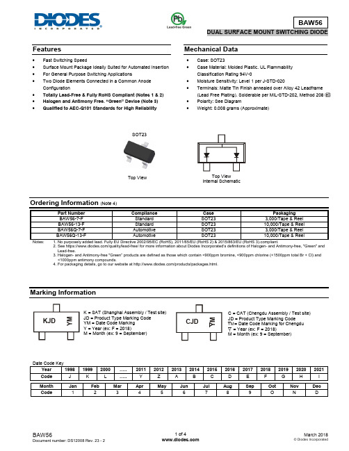
Features∙ Fast Switching Speed∙ Surface Mount Package Ideally Suited for Automated Insertion ∙ For General Purpose Switching Applications∙ Two Diode Elements Connected in a Common Anode Configuration∙ Totally Lead-Free & Fully RoHS Compliant (Notes 1 & 2) ∙ Halogen and Antimony Free. “Green” Device (Note 3) ∙ Qualified to AEC-Q101 Standards for High ReliabilityMechanical Data∙ Case: SOT23∙ Case Material: Molded Plastic. UL Flammability Classification Rating 94V-0∙ Moisture Sensitivity: Level 1 per J-STD-020∙ Terminals: Matte Tin Finish annealed over Alloy 42 Leadframe (Lead Free Plating). Solderable per MIL-STD-202, Method 208 ∙ Polarity: See Diagram∙Weight: 0.008 grams (Approximate)Ordering Information (Note 4)2. See https:///quality/lead-free/ for more information about Diodes Incorporated’s definitions of Halogen - and Antimony-free, "Green" and Lead-free.3. Halogen- and Antimony-free "Green” products are defined as those which contain <900ppm bromine, <900ppm chlorine (<1500ppm total Br + Cl) and <1000ppm antimony compounds.4. For packaging details, go to our website at /products/packages.html.Marking InformationTop ViewSOT23Top ViewInternal SchematicK = SAT (Shanghai Assembly / Test site) JD = Product Type Marking Code YM = Date Code Marking Y = Year (ex: F = 2018)M = Month (ex: 9 = September) C = CAT (Chengdu Assembly / Test site)JD = Product Type Marking Code= Date Code Marking for Chengdu = Year (ex: F = 2018) M = Month (ex: 9 = September)CJDY MKJD Y MYMY(@T = +25°C, unless otherwise specified.)Thermal CharacteristicsNotes: 5. Part mounted on FR-4 substrate PC board with 1inch squared, 2oz copper pad layout.6. Short duration pulse test used to minimize self-heating effect.400T , AMBIENT TEMPERATURE, (°C)Fig. 1 Power Derating Curve, Total Package A P P O W E R D I S S I P A T I O N (m W )D ,1000.110.010.001I , I N S T A N T A N E O U S F O R W A R D C U R R E N T (A )F V , INSTANTANEOUS FORWARD VOLTAGE (V)Fig. 2 Typical Forward Characteristics, Per Element F0.11101001,00010,000V , INSTANTANEOUS REVERSE VOLTAGE (V)Fig. 3 Typical Reverse Characteristics, Per Element R I , I N S T A N T A N E O U S R E V E R S E C U R R E N T (n A )R 0.00.20.40.60.81.81.61.41.21.02.0010204030C , T O T A L C A P A C I T A N C E (p F )T V , DC REVERSE VOLTAGE (V)Fig. 4 Total Capacitance vs. Reverse Voltage, Per Element RPackage Outline DimensionsPlease see /package-outlines.html for the latest version.Suggested Pad LayoutPlease see /package-outlines.html for the latest version.SOT23。
中兴通讯电源产品技术经理培训教材本部事业部电源系统部二00二年四月目录第一章中兴电源产品部简介 (1)一、中兴通讯电源产品部发展概括 (1)二、中兴通信电源产品种类 (2)第二章通信电源基础知识 (6)第一讲通信电源发展概况 (6)一、通信电源的现状和发展趋势 (6)二、通信设备对电源系统的一般要求 (9)第二讲组合通信电源系统结构及功能 (10)第三章中兴通信电源产品特色 (15)第一讲中兴整流器技术 (15)一、工作基本原理 (15)二、中兴整流器技术特点 (16)第二讲中兴组合电源系统特点 (18)可靠的三级防雷网络 (19)自下而上全分布式的三级监控网络 (20)完善的蓄电池管理 (22)灵活多样的组网方式 (22)第三讲组网方式 (23)第四章中兴组合通信电源产品系列介绍 (27)第一讲ZXD5000 100A整流模块及其组成的电源系统 (27)一、ZXD5000 100A整流模块介绍 (27)二、ZXDU3000、ZXDU1500通讯电源系统简介 (29)第二讲ZXD2400 50A整流模块及其组成的电源系统 (32)一、ZXD2400 50A整流模块介绍 (33)二、ZXDU600E、ZXDU400通讯电源系统简介 (34)第三讲ZXD1500 30A整流模块及其组成的电源系统 (37)一、ZXD1500 30A整流模块介绍 (37)二、ZXDU300(2米高机柜)ZXDU300(1.6米高机柜) 通讯电源系统简介 (39)第四讲ZXD800E 15A整流模块及其组成的电源系统 (41)一、ZXD800E 15A整流模块介绍 (41)二、ZXDU150、ZXDU75、ZXDU45通讯电源系统简介 (43)第五讲+24V组合通信电源系统 (46)第五章中兴UPS产品介绍 (47)ZXUPS S501 (47)ZXUPS S502 (48)ZXUPS S503 (48)ZXUPS S506 (48)ZXUPS S510 (49)ZXUPS M510 (49)ZXUPS M515 (49)ZXUPS M520 (50)ZXUPS M530 (50)ZXUPS L005 (50)ZXUPS L006 (50)第六章通信电源计算配置方法 (52)第七章通信电源市场概述 (55)第一讲国内主要通信电源厂家及其产品特色 (55)一、华为公司 (55)公司背景 (55)产品系列 (56)产品技术特点 (56)我司对策 (57)二、武汉洲际通信电源集团有限公司 (57)公司背景 (57)产品特点 (57)我司对策 (58)三、中达-斯米克电器电子有限公司 (58)公司背景 (58)产品系列 (58)与我司技术优、劣势对比 (59)我司对策 (59)四、珠江电信设备制造有限公司 (59)公司背景 (59)产品系列 (59)产品技术特点 (60)五、新西兰SWITCHTEC公司 (60)公司简介 (60)产品介绍 (60)我司对策 (61)六、亚澳通信电源有限公司 (61)公司概况 (61)产品技术特点简介 (62)我司对策 (62)七、动力源责任有限公司 (63)公司背景 (63)产品介绍 (63)产品优、劣势分析 (64)我司对策 (64)八、通力环电气有限公司 (65)公司背景 (65)产品系列 (65)产品特点 (66)九、意达公司 (67)产品系列 (67)产品技术特点 (68)第二讲我司电源产品市场拓展策略 (68)一、市场分类 (68)二、不同市场拓展策略 (69)三、2002年我司电源产品市场拓展策略 (70)第八章推荐参考书籍清单 (75)第一章中兴电源产品部简介导读:这一章主要介绍了中兴电源产品部的发展概况和现有的产品系列,是本教材的入门篇,各产品系列是本章掌握重点,同时关于产品部的发展、近几年的销售业绩等情况也经常用于客户交流中。
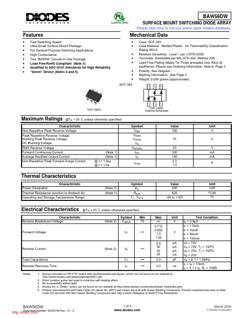
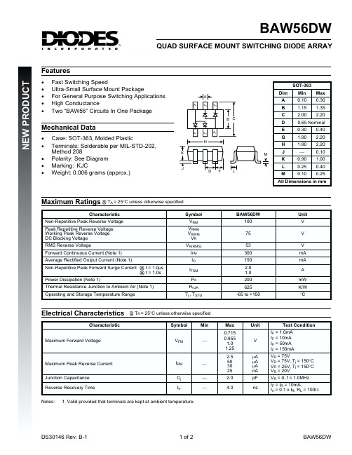
SURFACE MOUNT SWITCHING DIODE ARRAYFeatures• Fast Switching Speed• Ultra-Small Surface Mount Package• For General Purpose Switching Applications • High Conductance• Two “BAW56” Circuits In One Package • Lead Free/RoHS Compliant (Note 3)• Qualified to AEC-Q101 Standards for High Reliability •"Green" Device (Notes 4 and 5)Mechanical Data• Case: SOT-363• Case Material: Molded Plastic. UL Flammability Classification Rating 94V-0• Moisture Sensitivity: Level 1 per J-STD-020D• Terminals: Solderable per MIL-STD-202, Method 208• Lead Free Plating (Matte Tin Finish annealed over Alloy 42 leadframe). Please see Ordering Information: Note 6, Page 2 • Polarity: See Diagram• Marking Information: See Page 2 •Weight: 0.006 grams (approximate)SOT-363A1A 2C 2C 1C 2C 1 Internal SchematicTOP VIEWTOP VIEWMaximum Ratings @T A = 25°C unless otherwise specifiedCharacteristicSymbol Value Unit Non-Repetitive Peak Reverse Voltage V RM 100 V Peak Repetitive Reverse Voltage Working Peak Reverse Voltage DC Blocking VoltageV RRM V RWM V R 75 V RMS Reverse VoltageV R(RMS) 53 V Forward Continuous Current (Note 1)I FM 300 mA Average Rectified Output Current (Note 1)I O 150 mA Non-Repetitive Peak Forward Surge Current @ t = 1.0μs @ t = 1.0s I FSM2.0 1.0AThermal CharacteristicsCharacteristicSymbol Value Unit Power Dissipation (Note 1)P D 200 mW Thermal Resistance Junction to Ambient Air (Note 1)R θJA 625 °C/W Operating and Storage Temperature Range T J , T STG-65 to +150°CElectrical Characteristics @T A = 25°C unless otherwise specifiedCharacteristicSymbol Min Max Unit Test ConditionReverse Breakdown Voltage (Note 2)V (BR)R 75 ⎯ V I R = 2.5μA Forward VoltageV F⎯0.715 0.855 1.0 1.25 V I F = 1.0mA I F = 10mA I F = 50mA I F = 150mA Reverse Current (Note 2) I R ⎯ 2.5 50 30 25 μA μA μA nA V R = 75VV R = 75V, T J = 150°C V R = 25V, T J = 150°C V R = 20VTotal Capacitance C T ⎯ 2.0 pF V R = 0, f = 1.0MHz Reverse Recovery Timet rr⎯4.0nsI F = I R = 10mA,I rr = 0.1 x I R , R L = 100ΩNotes:1. Device mounted on FR-4 PC board with recommended pad layout, which can be found on our website at/datasheets/ap02001.pdf.2. Short duration pulse test used to minimize self-heating effect.3. No purposefully added lead.4. Diodes Inc.'s "Green" policy can be found on our website at /products/lead_free/index.php.5. Product manufactured with Date Code UO (week 40, 2007) and newer are built with Green Molding Compound. Product manufactured prior to Date Code UO are built with Non-Green Molding Compound and may contain Halogens or Sb2O3 Fire Retardants.BAW56DWDocument number: DS30146 Rev. 10 - 21 of 3March 2008© Diodes Incorporated/Please click here to visit our online spice models database.0.110.010.001I , I N S T A N T A N E O U S F O R W A R D C U R R E N T (A )F V , INSTANTANEOUS FORWARD VOLTAGE (V)Fig. 2 Typical Forward Characteristics, Per Element F300BAW56DWDocument number: DS30146 Rev. 10 - 22 of 3March 2008© Diodes Incorporated0501001502002502505075100125150P , P O W E R D I S S I P A T I O N (m W )D T , AMBIENT TEMPERATURE (C)A °Fig. 1 Power Derating Curve, Total Package Note 10.00.20.40.60.81.81.61.41.21.02.0010204030C , T O T A L C A P A C I T A N C E (p F )T V , DC REVERSE VOLTAGE (V)Fig. 4 Total Capacitance vs. Reverse Voltage, Per Element R101001,00010,000020406080100V , INSTANTANEOUS REVERSE VOLTAGE (V)Fig. 3 Typical Reverse Characteristics, Per Element R I , I N S T A N T A N E O U S R E V E R S E C U R R E N T (n A )ROrdering Information (Note 6)Part Number Case Packaging BAW56DW-7-FSOT-363 3000/Tape & ReelNotes: 6. For packaging details, go to our website at /datasheets/ap02007.pdf.Marking InformationKJC YMK J C Y MKJC = Product Type Marking Code YM = Date Code Marking Y = Year ex: N = 2002 M = Month ex: 9 = SeptemberDate Code KeyYear 2000 2001 2002 2003 2004 2005 2006 2007 2008 2009 2010 2011 2012Code L M N P R S T U V W X Y ZMonth Jan Feb Mar AprMay Jun Jul Aug Sep Oct Nov DecCode 1 2 3 4 5 6 7 8 9 O N D/Package Outline DimensionsBAW56DWDocument number: DS30146 Rev. 10 - 23 of 3March 2008© Diodes IncorporatedSuggested Pad LayoutIMPORTANT NOTICEDiodes Incorporated and its subsidiaries reserve the right to make modifications, enhancements, improvements, corrections or other changes without further notice to any product herein. Diodes Incorporated does not assume any liability arising out of the application or use of any product described herein; neither does it convey any license under its patent rights, nor the rights of others. The user of products in such applications shall assume all risks of such use and will agree to hold Diodes Incorporated and all the companies whose products are represented on our website, harmless against all damages.LIFE SUPPORTDiodes Incorporated products are not authorized for use as critical components in life support devices or systems without the expressed written approval of the President of Diodes Incorporated.SOT-363Dim Min Max A 0.10 0.30 B 1.15 1.35 C 2.00 2.20 D 0.65 Nominal F 0.30 0.40 H 1.80 2.20 J ⎯ 0.10 K 0.90 1.00 L 0.25 0.40 M 0.10 0.25α0° 8° All Dimensions in mmXZYCEEG Dimensions Value (in mm)Z 2.5 G 1.3 X 0.42 Y 0.6 C 1.9 E 0.65/分销商库存信息:DIODESBAW56DW-7-F BAW56DW-7。
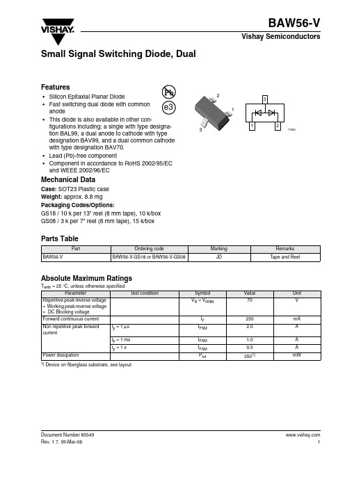
BAW56-VDocument Number 85549Rev. 1.7, 09-Mar-06Vishay Semiconductors1Small Signal Switching Diode, DualFeatures•Silicon Epitaxial Planar Diode•Fast switching dual diode with commonanode•This diode is also available in other con-figurations including: a single with type designa-tion BAL99, a dual anode to cathode with type designation BAV99, and a dual common cathode with type designation BAV70. •Lead (Pb)-free component•Component in accordance to RoHS 2002/95/EC and WEEE 2002/96/ECMechanical DataCase: SOT23 Plastic case Weight: approx. 8.8 mgPackaging Codes/Options:GS18 / 10 k per 13" reel (8 mm tape), 10 k/box GS08 / 3 k per 7" reel (8 mm tape), 15 k/boxParts TableAbsolute Maximum RatingsT amb = 25°C, unless otherwise specified1) Device on fiberglass substrate, see layoutPartOrdering codeMarking Remarks BAW56-VBAW56-V-GS18 or BAW56-V-GS08JDTape and ReelParameterT est condition Symbol Value Unit Repetitive peak reverse voltage = Working peak reverse voltage = DC Blocking voltage V R = V RRM70VForward continuous current I F 250mA Non repetitive peak forward currentt p = 1 μs I FSM 2.0A t p = 1 ms I FSM 1.0A t p = 1 sI FSM 0.5A Power dissipationP tot3501)mW 2Document Number 85549Rev. 1.7, 09-Mar-06BAW56-VVishay Semiconductors Thermal CharacteristicsT amb = 25°C, unless otherwise specified1) Device on fiberglass substrate, see layoutElectrical CharacteristicsT amb = 25°C, unless otherwise specifiedTypical CharacteristicsT amb = 25°C, unless otherwise specifiedParameterTest condition Symbol Value Unit Thermal resistance junction to ambiant airR thJA 430K/W Junction temperature T j 150°C Storage temperature rangeT stg- 65 to + 150°CParameterTest conditionSymbol MinTyp.Max Unit Forward voltageI F = 1 mA V F 715mV I F = 10 mA V F 855mV I F = 50 mA V F 1000mV I F = 150 mAV F 1250mV Reverse currentV R= 70 VI R 2.5µA V R = 70 V , T j = 150°C I R 100µA V R = 25 V , T j = 150°CI R 30µA Diode capacitance V F = V R = 0, f = 1 MHz C tot 2pF Reverse recovery timeI F = 10 mA to I R = 1 mA, V R = 6 V , R L = 100 Ωt rr6nsFigure 1. Forward Current vs. Forward VoltageV F -For w ard V oltage (V )14356Figure 2. Peak forward current I FM = f (t p )BAW56-VDocument Number 85549Rev. 1.7, 09-Mar-06Vishay Semiconductors3Package Dimensions in mm (Inches) 4Document Number 85549 Rev. 1.7, 09-Mar-06BAW56-VVishay SemiconductorsOzone Depleting Substances Policy StatementIt is the policy of Vishay Semiconductor GmbH to1.Meet all present and future national and international statutory requirements.2.Regularly and continuously improve the performance of our products, processes, distribution and operatingsystems with respect to their impact on the health and safety of our employees and the public, as well as their impact on the environment.It is particular concern to control or eliminate releases of those substances into the atmosphere which are known as ozone depleting substances (ODSs).The Montreal Protocol (1987) and its London Amendments (1990) intend to severely restrict the use of ODSs and forbid their use within the next ten years. Various national and international initiatives are pressing for an earlier ban on these substances.Vishay Semiconductor GmbH has been able to use its policy of continuous improvements to eliminate the use of ODSs listed in the following documents.1.Annex A, B and list of transitional substances of the Montreal Protocol and the London Amendmentsrespectively2.Class I and II ozone depleting substances in the Clean Air Act Amendments of 1990 by the EnvironmentalProtection Agency (EPA) in the USA3.Council Decision 88/540/EEC and 91/690/EEC Annex A, B and C (transitional substances) respectively. Vishay Semiconductor GmbH can certify that our semiconductors are not manufactured with ozone depleting substances and do not contain such substances.We reserve the right to make changes to improve technical designand may do so without further notice.Parameters can vary in different applications. All operating parameters must be validated for each customer application by the customer. Should the buyer use Vishay Semiconductors products for any unintended or unauthorized application, the buyer shall indemnify Vishay Semiconductors against all claims, costs, damages, and expenses, arising out of, directly or indirectly, any claim of personal damage, injury or death associated with such unintended or unauthorized use.Vishay Semiconductor GmbH, P.O.B. 3535, D-74025 Heilbronn, GermanyDocument Number: 91000Revision: 18-Jul-081DisclaimerLegal Disclaimer NoticeVishayAll product specifications and data are subject to change without notice.Vishay Intertechnology, Inc., its affiliates, agents, and employees, and all persons acting on its or their behalf (collectively, “Vishay”), disclaim any and all liability for any errors, inaccuracies or incompleteness contained herein or in any other disclosure relating to any product.Vishay disclaims any and all liability arising out of the use or application of any product described herein or of any information provided herein to the maximum extent permitted by law. The product specifications do not expand or otherwise modify Vishay’s terms and conditions of purchase, including but not limited to the warranty expressed therein, which apply to these products.No license, express or implied, by estoppel or otherwise, to any intellectual property rights is granted by this document or by any conduct of Vishay.The products shown herein are not designed for use in medical, life-saving, or life-sustaining applications unless otherwise expressly indicated. Customers using or selling Vishay products not expressly indicated for use in such applications do so entirely at their own risk and agree to fully indemnify Vishay for any damages arising or resulting from such use or sale. Please contact authorized Vishay personnel to obtain written terms and conditions regarding products designed for such applications.Product names and markings noted herein may be trademarks of their respective owners.元器件交易网。

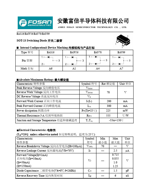
安徽富信半导体科技有限公司ANHUI FOSAN SEMICONDUCTOR TECHNOLOGY CO.,LTD.BAS16/BAW56/BAV70/BAV99SOT-23Switching Diode 开关二极管▉Internal Configuration&DeviceMarking 内部结构与产品打标Type 型号BAS16BAW56BAV70BAV99Pin 管脚Mark 打标A6A1A4A7▉AbsoluteMaximum Ratings 最大额定值Characteristic 特性参数Symbol 符号Rat 额定值Unit 单位Peak Reverse V oltage 反向峰值电压V RRM 70V Reverse Work Voltage 反向工作电压V RWMDC Reverse Voltage 直流反向电压V R Forward Work Current 正向工作电流I F (I O )200mA Peak Forward Current 正向峰值电流I FM300mA Power dissipation 耗散功率P D (Ta=25℃)225mW Thermal Resistance J-A 结到环境热阻R θJA 555℃/WJunction and Storage Temperature 结温和储藏温度T J ,T stg-55to+150℃■Electrical Characteristics 电特性(T A =25℃unless otherwise noted 如无特殊说明,温度为25℃)Characteristic 特性参数Symbol 符号Min 最小值Max 最大值Unit 单位Reverse Breakdown Voltage 反向击穿电压(I R =100µA)V (BR)70—V Reverse Leakage Current 反向漏电流(V R =70V)I R — 2.5µA Forward V oltage(I F =1mA)正向电压(I F =10mA)(I F =50mA)(I F =150mA)V F —0.7150.8551.01.25V Diode Capacitance 二极管电容(V R =0V,f=1MHz)C D— 1.5pF Reverse Recovery Time 反向恢复时间T rr—6nSANHUI FOSAN SEMICONDUCTOR TECHNOLOGY CO.,LTD.BAS16/BAW56/BAV70/BAV99■Typical Characteristic Curve典型特性曲线ANHUI FOSAN SEMICONDUCTOR TECHNOLOGY CO.,LTD.BAS16/BAW56/BAV70/BAV99■Dimension外形封装尺寸Symbol Dimensions In Millimeters Dimensions In Inches Min Max Min Max A 0.900 1.1500.0350.045A10.0000.1000.0000.004A20.900 1.0500.0350.041b 0.3000.5000.0120.020c 0.0800.1500.0030.006D 2.800 3.0000.1100.118E 1.200 1.4000.0500.055E1 2.2502.5500.0890.100e 0.950TYP0.037TYPe1 1.8002.0000.0710.079L 0.550REF0.022REFL10.3000.5000.0120.020θ0o8o 0o8o。
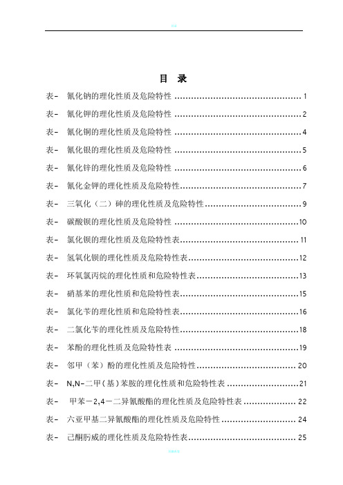
目录表-氰化钠的理化性质及危险特性 (1)表-氰化钾的理化性质及危险特性 (2)表-氰化铜的理化性质及危险特性 (4)表-氰化银的理化性质及危险特性 (5)表-氰化锌的理化性质及危险特性 (6)表-氰化金钾的理化性质及危险特性 (7)表-三氧化(二)砷的理化性质及危险特性 (9)表-碳酸钡的理化性质及危险特性 (10)表-氯化钡的理化性质及危险特性表 (11)表-氢氧化钡的理化性质及危险特性表 (12)表-环氧氯丙烷的理化性质和危险特性表 (13)表-硝基苯的理化性质和危险特性表 (15)表-氯化苄的理化性质和危险特性表 (16)表-二氯化苄的理化性质及危险特性 (18)表-苯酚的理化性质及危险特性表 (19)表-邻甲(苯)酚的理化性质及危险特性 (20)表-N,N-二甲(基)苯胺的理化性质和危险特性表 (21)表- 甲苯-2,4-二异氰酸酯的理化性质及危险特性表 (22)表-六亚甲基二异氰酸酯的理化性质及危险特性 (24)表-己酮肟威的理化性质及危险特性表 (25)表-克百威[含量>10%]的理化性质及危险特性表 (27)表-自克威[含量>25%]的理化性质及危险特性表 (28)表-间异丙威的理化性质及危险特性表 (30)表-杀线威的理化性质及危险特性表 (31)表-敌蝇威[含量>50%]的理化性质及危险特性表 (32)表-涕灭威的理化性质及危险特性表 (33)表-腈叉威的理化性质及危险特性表 (34)表-恶虫威[含量>65%]的理化性质及危险特性表 (36)表-异索威[含量>20%]的理化性质及危险特性表 (37)表-硒粉的理化性质及危险特性 (38)表-氧化钡的理化性质及危险特性表 (39)表-一氧化铅的理化性质和危险特性表 (40)表-四氧化(三)铅的理化性质和危险特性表 (42)表-硫酸汞的理化性质和危险特性表 (43)表-硝酸亚汞的理化性质和危险特性表 (44)表-氟化铵的理化性质及危险特性表 (45)表-氟化钠的理化性质及危险特性 (46)表-氟化钾的理化性质及危险特性 (48)表-氟化钡的理化性质及危险特性 (49)表-氟硅酸钠的理化性质和危险特性表 (50)表-氟锆酸钾的理化性质及危险特性 (51)表-二氯甲烷的理化性质及危险特性 (53)表-三氯甲烷的理化性质及危险特性表 (55)表-四氯化碳的理化性质及危险特性 (56)表-1,1,1-三氯乙烷的理化性质及危险特性表 (58)表1,1,2-三氯乙烷的理化性质及危险特性表 (59)表- 1,1,2,2-四氯乙烷的理化性质和危险特性表 (60)表-溴代乙烷的理化性质和危险特性表 (61)表-三氯乙烯的理化性质及危险特性表 (63)表-四氯乙烯的理化性质及危险特性表 (64)表-十二硫醇的理化性质和危险特性表 (65)表-乙二醇丁醚的理化性质及危险特性表 (66)表-水杨醛的理化性质和危险特性表 (68)表-二苯甲烷-4,4’-二异氰酸酯的理化性质及危险特性 (69)表-异佛尔酮二异氰酸酯的理化性质及危险特性表 (70)表-邻二氯苯的理化性质和危险特性表 (71)表-3,4-二氯苄基氯的理化性质及危险特性 (73)表-对甲苯磺酰氯的理化性质和危险特性表 (74)表-邻硝基(苯)酚的理化性质和危险特性表 (75)表-对硝基(苯)酚的理化性质和危险特性表 (76)表-邻氨基(苯)酚的理化性质和危险特性表 (77)表-间氨基(苯)酚的理化性质和危险特性表 (79)表-邻苯二酚的理化性质及危险特性表 (81)表-间苯二酚的理化性质和危险特性表 (82)表-对苯二酚的理化性质及危险特性表 (83)表-间苯三酚的理化性质和危险特性表 (84)表-丙烯酰胺的理化性质及危险特性表 (85)表-苯胺的理化性质和危险特性表 (87)表-邻苯二胺的理化性质和危险特性表 (88)表-间苯二胺的理化性质和危险特性表 (89)表-对苯二胺的理化性质和危险特性表 (90)表-苯肼的理化性质和危险特性表 (91)表-硫脲的理化性质及危险特性表 (93)表-苯醌的理化性质及危险特性表 (94)表-α-萘乙酸的理化性质和危险特性表 (95)表-α-萘胺的理化性质和危险特性表 (96)表-盐酸-1-萘乙二胺的理化性质和危险特性表 (97)表-喹啉的理化性质和危险特性表 (98)表-乙酸铅的理化性质和危险特性表 (100)表-酒石酸锑钾的理化性质和危险特性表 (101)表-二丁基二月桂酸锡的理化性质和危险特性表 (102)表-辛酸亚锡的理化性质和危险特性表 (104)表-三苯(基)磷的理化性质及危险特性表 (105)表-煤焦沥青的理化性质及危险特性 (106)表-2,4-滴[含量>75%]的理化性质和危险特性表 (107)表-1,2,2-三氯三氟乙烷的理化性质及危险特性 (108)表-氰化钠的理化性质及危险特性表-氰化钾的理化性质及危险特性表-氰化铜的理化性质及危险特性表-氰化银的理化性质及危险特性表-氰化锌的理化性质及危险特性表-氰化金钾的理化性质及危险特性表-三氧化(二)砷的理化性质及危险特性表-碳酸钡的理化性质及危险特性表-氯化钡的理化性质及危险特性表表-氢氧化钡的理化性质及危险特性表表-环氧氯丙烷的理化性质和危险特性表表-硝基苯的理化性质和危险特性表表-氯化苄的理化性质和危险特性表表-二氯化苄的理化性质及危险特性表-苯酚的理化性质及危险特性表表-邻甲(苯)酚的理化性质及危险特性表-N,N-二甲(基)苯胺的理化性质和危险特性表表- 甲苯-2,4-二异氰酸酯的理化性质及危险特性表表-六亚甲基二异氰酸酯的理化性质及危险特性表-己酮肟威的理化性质及危险特性表表-灭害威的理化性质及危险特性表表-克百威[含量>10%]的理化性质及危险特性表表-自克威[含量>25%]的理化性质及危险特性表表-间异丙威的理化性质及危险特性表表-杀线威的理化性质及危险特性表表-敌蝇威[含量>50%]的理化性质及危险特性表表-涕灭威的理化性质及危险特性表表-腈叉威的理化性质及危险特性表表-恶虫威[含量>65%]的理化性质及危险特性表表-异索威[含量>20%]的理化性质及危险特性表表-硒粉的理化性质及危险特性表-氧化钡的理化性质及危险特性表表-一氧化铅的理化性质和危险特性表表-四氧化(三)铅的理化性质和危险特性表表-硫酸汞的理化性质和危险特性表表-硝酸亚汞的理化性质和危险特性表表-氟化铵的理化性质及危险特性表。
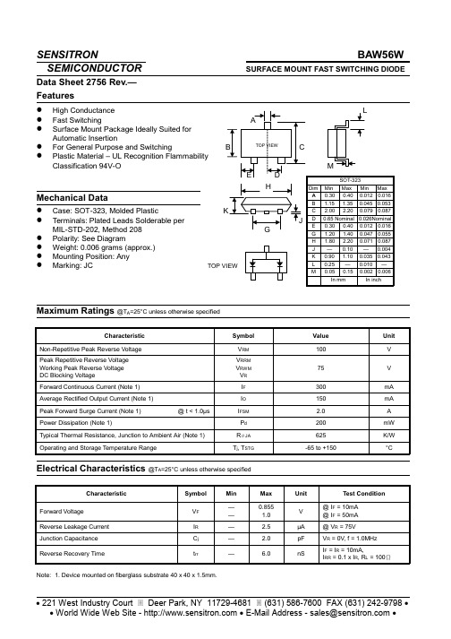
0 * % $ *,= = - > - - - ( ) ? *+*, "# = 6 / 9# "* * * " = - 0 - 8 -@AB ( ) ( ) 7=-4- 8- C 8 ( --& . ) # % : ,$* #: * D- C D- C元器件交易网110100100010,0000100200I ,L E A K A G E C U R R E N T (n A )R T ,JUNCTION TEMPERATURE (°C)Fig.2Leakage Current vs Junction Temperaturej 101.010010000.10.01012I ,I N S T A N T A N E O U S F O R W A R D C U R R E N T (m A )F V ,INSTANTANEOUS FORWARD VOLTAGE (V)Fig.1Forward CharacteristicsF元器件交易网元器件交易网SENSITRONSEMICONDUCTORTECHNICAL DATADISCLAIMER:1- The information given herein, including the specifications and dimensions, is subject to change without prior notice to improve productcharacteristics. Before ordering, purchasers are advised to contact the Sensitron Semiconductor sales department for the latest versionof the datasheet(s).2- In cases where extremely high reliability is required (such as use in nuclear power control, aerospace and aviation, traffic equipment,medical equipment, and safety equipment), safety should be ensured by using semiconductor devices that feature assured safety or bymeans of users’ fail-safe precautions or other arrangement.3- In no event shall Sensitron Semiconductor be liable for any damages that may result from an accident or any other cause duringoperation of the user’s units according to the datasheet(s). Sensitron Semiconductor assumes no responsibility for any intellectualproperty claims or any other problems that may result from applications of information, products or circuits described in the datasheets.4- In no event shall Sensitron Semiconductor be liable for any failure in a semiconductor device or any secondary damage resulting fromuse at a value exceeding the absolute maximum rating.5- No license is granted by the datasheet(s) under any patents or other rights of any third party or Sensitron Semiconductor.6- The datasheet(s) may not be reproduced or duplicated, in any form, in whole or part, without the expressed written permission ofSensitron Semiconductor.7- The products (technologies) described in the datasheet(s) are not to be provided to any party whose purpose in their application willhinder maintenance of international peace and safety nor are they to be applied to that purpose by their direct purchasers or any thirdparty. When exporting these products (technologies), the necessary procedures are to be taken in accordance with related laws andregulations.• 221 West Industry Court Deer Park, NY 11729-4681 (631) 586-7600 FAX (631) 242-9798 •• World Wide Web - • E-Mail Address - sales@ •。


Handling of gears in a milling centerSectional diagramCleaning UnitFor the exact size of the required accessories, availability of this size and the designation and ID, please refer to the additional views at the end of the size in question. You will find more detailed information on our accessory range in the “Accessories” catalog section.Perfectly adaptable to smooth surfaces, with dampening effect during attachment and The indicated times depend on the flow rate and pressure of the drive medium and the Workpiece weightThe recommended workpiece weight is calculated for a force-fit connection, indicated nominal flow rate and pressure as well as a safety factor of 2 against the weight of the acceleration of gravity g.Suction cup dimensionsDescription ID D H SSuction padSND 30-G1/4030913534 mm20 mm3 mmSND 80-G1/4030913689 mm40 mm7.6 mmSND 125-G1/40309137135 mm48 mm12.5 mmYou can find more detailed information and individual parts of the above-mentioned accessories in the “Accessories” catalog section.Suction cup dimensionsDescription ID D H SSuction padSND 30-G1/4030913534 mm20 mm3 mmSND 80-G1/4030913689 mm40 mm7.6 mmSND 125-G1/40309137135 mm48 mm12.5 mmYou can find more detailed information and individual parts of the above-mentioned accessories in the “Accessories” catalog section.Suction cup dimensionsDescription ID D H SSuction padSND 30-G1/4030913534 mm20 mm3 mmSND 80-G1/4030913689 mm40 mm7.6 mmSND 125-G1/40309137135 mm48 mm12.5 mmYou can find more detailed information and individual parts of the above-mentioned accessories in the “Accessories” catalog section.。

8吨豪沃运输车军用参数表摘要:I.引言- 介绍8 吨豪沃运输车军用参数表II.车辆基本参数- 车辆型号- 整备质量- 最高车速- 续航里程III.军事性能参数- 越野能力- 最大爬坡度- 涉水深度- 载重量IV.安全性能参数- 制动系统- 安全气囊- 防抱死制动系统(ABS)V.驾驶室与舒适性参数- 驾驶室类型- 座椅布局- 车载空调- 车载娱乐系统VI.动力与悬挂参数- 发动机类型与功率- 变速器类型- 悬挂系统VII.总结- 总结8 吨豪沃运输车军用参数表的特点与优势正文:在我国军事领域,运输车辆在物资运输和兵员调动等方面发挥着至关重要的作用。
今天,我们将详细介绍一款具有优异性能的8 吨豪沃运输车军用参数表,让大家对该车型有更深入的了解。
I.引言8 吨豪沃运输车是一款我国自主研发的军用运输车辆,凭借其出色的性能和实用性,广泛应用于军队物资运输、战场支援等任务。
接下来,我们将从车辆基本参数、军事性能参数、安全性能参数、驾驶室与舒适性参数、动力与悬挂参数五个方面详细介绍这款车型。
II.车辆基本参数8 吨豪沃运输车的车辆型号为HOWO,整备质量为8 吨,最高车速可达100 公里/小时,续航里程超过800 公里。
III.军事性能参数在军事性能方面,8 吨豪沃运输车表现出色。
其越野能力强大,可适应各种复杂地形;最大爬坡度达到30%,涉水深度达到0.8 米;载重量高达8 吨,满足军队物资运输的需求。
IV.安全性能参数为确保驾驶员及车辆安全,8 吨豪沃运输车配备了完善的安全系统。
制动系统采用双回路气制动,可有效缩短制动距离;车辆配备安全气囊,提高碰撞安全性;同时,车辆还配备了防抱死制动系统(ABS),使车辆在紧急制动时仍能保持良好的转向性能。
V.驾驶室与舒适性参数8 吨豪沃运输车的驾驶室采用人性化设计,座椅布局宽敞舒适,可有效减轻驾驶员的疲劳感。
车载空调系统可随时调节驾驶室温度,为驾驶员创造舒适的驾驶环境。
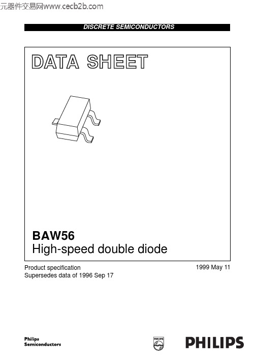
DATASHEETProduct specificationSupersedes data of 1996Sep 171999May 11DISCRETE SEMICONDUCTORSBAW56High-speed double diodebook, halfpageM3D088High-speed double diodeBAW56FEATURES•Small plastic SMD package •High switching speed: max.4ns •Continuous reverse voltage:max.75V•Repetitive peak reverse voltage:max.85V•Repetitive peak forward current:max. 450mA.APPLICATIONS•High-speed switching in thick and thin-film circuits.DESCRIPTIONThe BAW56 consists of twohigh-speed switching diodes with common anodes, fabricated in planar technology, and encapsulated in the small SOT23 plastic SMD package.PINNINGPIN DESCRIPTION 1cathode (k1)2cathode (k2)3common anodeFig.1 Simplified outline (SOT23) and symbol.Marking code: A1p =made in Hong Kong; A1t =made in Malaysia.handbook, 4 columns213MAM206Top view213LIMITING VALUESIn accordance with the Absolute Maximum Rating System (IEC 134).Note1.Device mounted on an FR4 printed-circuit board.SYMBOL PARAMETERCONDITIONSMIN.MAX.UNITPer diode V RRM repetitive peak reverse voltage −85V V R continuous reverse voltage −75V I Fcontinuous forward currentsingle diode loaded; note 1;see Fig.2−215mA double diode loaded; note 1;see Fig.2−125mA I FRM repetitive peak forward current −450mAI FSMnon-repetitive peak forward currentsquare wave; T j =25°C prior to surge; see Fig.4t =1µs −4A t =1ms −1A t =1s−0.5A P tot total power dissipation T amb =25°C; note 1−250mW T stg storage temperature −65+150°C T j junction temperature−150°CHigh-speed double diodeBAW56ELECTRICAL CHARACTERISTICS T j =25°C unless otherwise specified.THERMAL CHARACTERISTICS Note1.Device mounted on an FR4 printed-circuit board.SYMBOL PARAMETERCONDITIONSMAX.UNITPer diode V Fforward voltagesee Fig.3I F =1mA 715mV I F =10mA 855mV I F =50mA 1V I F =150mA1.25V I Rreverse currentsee Fig.5V R =25V 30nA V R =75V1µA V R =25V; T j =150°C 30µA V R =75V; T j =150°C50µA C d diode capacitance f =1MHz; V R =0; see Fig.62pF t rrreverse recovery timewhen switched from I F =10mA to I R =10mA; R L =100Ω;measured at I R =1mA; see Fig.74nsV frforward recovery voltage when switched from I F =10mA;t r =20ns; see Fig.81.75VSYMBOL PARAMETERCONDITIONSVALUE UNIT R th j-tp thermal resistance from junction to tie-point 360K/W R th j-a thermal resistance from junction to ambientnote 1500K/WHigh-speed double diodeBAW56GRAPHICAL DATADevice mounted on an FR4 printed-circuit board.Fig.2Maximum permissible continuous forward current as a function of ambient temperature.02003000100200MBD033100I F (mA)T ( C)ambosingle diode loadeddouble diode loaded(1)T j =150°C; typical values.(2)T j =25°C; typical values.(3)T j =25°C; maximum values.Fig.3Forward current as a function of forward voltage.handbook, halfpage02300I F(mA)100200MBG3821V F (V)(1)(3)(2)Fig.4 Maximum permissible non-repetitive peak forward current as a function of pulse duration.Based on square wave currents.T j =25°C prior to surge.handbook, full pagewidthMBG70410t p (µs)1I FSM (A)10210−1104102103101High-speed double diode BAW56Fig.5Reverse current as a function of junction temperature.105104102000MGA884100T ( C)jo I R (nA)10310275 V25 VtypmaxV = 75 V RtypFig.6Diode capacitance as a function of reverse voltage; typical values.f =1MHz; T j =25°C.handbook, halfpage025V R (V)2.50.5MBH1911.01.52.05C d (pF)101520High-speed double diode BAW56Fig.7 Reverse recovery voltage test circuit and waveforms.handbook, full pagewidtht rr(1)I F toutput signalt rtt p10%90%V Rinput signal V = V I x R R F SR = 50SΩI FD.U.T.R = 50iΩSAMPLING OSCILLOSCOPEMGA881(1)I R =1mA.Fig.8 Forward recovery voltage test circuit and waveforms.t rtt p10%90%Iinputsignal R = 50SΩIR = 50iΩOSCILLOSCOPEΩ1 k Ω450 D.U.T.MGA882V frtoutput signalVHigh-speed double diodeBAW56PACKAGE OUTLINEUNIT A 1max.b p c D E e 1H E L p Q w v REFERENCESOUTLINE VERSION EUROPEAN PROJECTIONISSUE DATE 97-02-28IECJEDECEIAJmm0.10.480.380.150.093.02.81.41.20.95e 1.92.52.10.550.450.10.2DIMENSIONS (mm are the original dimensions)0.450.15SOT23b pD e 1eAA 1L pQdetail XH EE w M v M ABAB 01 2 mmscaleA 1.10.9cX123Plastic surface mounted package; 3 leadsSOT23High-speed double diode BAW56DEFINITIONSData Sheet StatusObjective specification This data sheet contains target or goal specifications for product development. Preliminary specification This data sheet contains preliminary data; supplementary data may be published later. Product specification This data sheet contains final product specifications.Limiting valuesLimiting values given are in accordance with the Absolute Maximum Rating System (IEC 134). Stress above one or more of the limiting values may cause permanent damage to the device. These are stress ratings only and operation of the device at these or at any other conditions above those given in the Characteristics sections of the specification is not implied. Exposure to limiting values for extended periods may affect device reliability.Application informationWhere application information is given, it is advisory and does not form part of the specification.LIFE SUPPORT APPLICATIONSThese products are not designed for use in life support appliances, devices, or systems where malfunction of these products can reasonably be expected to result in personal injury. Philips customers using or selling these products for use in such applications do so at their own risk and agree to fully indemnify Philips for any damages resulting from such improper use or sale.High-speed double diode BAW56NOTESHigh-speed double diode BAW56NOTESPhilips Semiconductors Product specification High-speed double diode BAW56NOTES1999May1111© Philips Electronics N.V. SCA All rights are reserved. Reproduction in whole or in part is prohibited without the prior written consent of the copyright owner.The information presented in this document does not form part of any quotation or contract, is believed to be accurate and reliable and may be changed without notice. No liability will be accepted by the publisher for any consequence of its use. Publication thereof does not convey nor imply any license under patent- or other industrial or intellectual property rights.Internet: 199964Philips Semiconductors – a worldwide company Netherlands: Postbus 90050, 5600PB EINDHOVEN, Bldg.VB,Tel.+31402782785,Fax.+31402788399New Zealand: 2Wagener Place, C.P.O.Box 1041, AUCKLAND,Tel.+6498494160,Fax.+6498497811Norway: Box 1, Manglerud 0612, OSLO,Tel.+4722748000,Fax.+4722748341Pakistan: see Singapore Philippines: Philips Semiconductors Philippines Inc.,106Valero St.Salcedo Village, P.O.Box 2108MCC,MAKATI,Metro MANILA, Tel.+6328166380,Fax.+6328173474Poland: Ul.Lukiska 10, PL 04-123WARSZAWA,Tel.+48226122831,Fax.+48226122327Portugal: see Spain Romania: see Italy Russia: Philips Russia, atcheva 35A, 119048MOSCOW,Tel.+70957556918,Fax.+70957556919Singapore: Lorong 1, Toa Payoh, SINGAPORE 319762,Tel.+653502538,Fax.+652516500Slovakia: see Austria Slovenia: see Italy South Africa: S.A. PHILIPS Pty Ltd., 195-215Main Road Martindale,2092JOHANNESBURG, P.O.Box 58088 Newville 2114,Tel.+27114715401,Fax.+27114715398South America: Al.Vicente Pinzon,173, 6th floor,04547-130SÃO PAULO,SP, Brazil,Tel.+55118212333,Fax.+55118212382Spain: Balmes 22, 08007BARCELONA,Tel.+34933016312,Fax.+34933014107Sweden: Kottbygatan 7, Akalla, S-16485STOCKHOLM,Tel.+46859852000,Fax.+46859852745Switzerland: Allmendstrasse 140, CH-8027ZÜRICH,Tel.+4114882741Fax.+4114883263Taiwan: Philips Semiconductors, 6F, No.96, Chien Kuo N.Rd.,Sec.1,TAIPEI, Taiwan Tel.+886221342886,Fax.+886221342874Thailand: PHILIPS ELECTRONICS (THAILAND) Ltd.,209/2Sanpavuth-Bangna Road Prakanong, BANGKOK 10260,Tel.+6627454090,Fax.+6623980793Turkey: Yukari Dudullu, Org. San. Blg., 2.Cad. Nr. 28 81260Umraniye,ISTANBUL, Tel.+902165221500,Fax.+902165221813Ukraine : PHILIPS UKRAINE, 4Patrice Lumumba str., Building B, Floor 7,252042KIEV, Tel.+380442642776, Fax. +380442680461United Kingdom: Philips Semiconductors Ltd., 276Bath Road, Hayes,MIDDLESEX UB35BX, Tel.+441817305000,Fax.+441817548421United States: 811East Arques Avenue, SUNNYVALE, CA 94088-3409,Tel.+18002347381, Fax.+18009430087Uruguay: see South America Vietnam: see Singapore Yugoslavia: PHILIPS, Trg N. Pasica 5/v, 11000BEOGRAD,Tel.+38111625344,Fax.+38111635777For all other countries apply to: Philips Semiconductors,International Marketing &Sales Communications, Building BE-p, P.O.Box 218,5600MD EINDHOVEN, The Netherlands,Fax.+31402724825Argentina: see South AmericaAustralia: 34 Waterloo Road, NORTH RYDE, NSW 2113,Tel.+61298054455,Fax.+61298054466Austria:Computerstr. 6, A-1101 WIEN, P.O. Box 213,Tel.+431601011248, Fax.+431601011210Belarus: Hotel Minsk Business Center, Bld.3, r.1211, Volodarski Str.6,220050MINSK, Tel.+375172200733,Fax.+375172200773Belgium: see The NetherlandsBrazil:see South AmericaBulgaria:Philips Bulgaria Ltd., Energoproject, 15th floor,51James Bourchier Blvd., 1407SOFIA,Tel.+3592689211,Fax.+3592689102Canada: PHILIPS SEMICONDUCTORS/COMPONENTS,Tel.+18002347381, Fax.+18009430087China/Hong Kong: 501Hong Kong Industrial Technology Centre,72Tat Chee Avenue, Kowloon Tong, HONG KONG,Tel.+852********,Fax.+852********Colombia: see South AmericaCzech Republic: see AustriaDenmark: Sydhavnsgade 23, 1780COPENHAGEN V,Tel.+4533293333,Fax.+4533293905Finland: Sinikalliontie 3, FIN-02630ESPOO,Tel.+3589615800,Fax.+358961580920France: 51Rue Carnot, BP317, 92156SURESNES Cedex,Tel.+33140996161,Fax.+33140996427Germany: Hammerbrookstraße 69, D-20097HAMBURG,Tel.+4940235360,Fax.+494023536300Hungary:see AustriaIndia: Philips INDIA Ltd, Band Box Building, 2nd floor,254-D,Dr.Annie Besant Road, Worli, MUMBAI 400025,Tel.+91224938541,Fax.+91224930966Indonesia: PT Philips Development Corporation, Semiconductors Division,Gedung Philips, Jl. Buncit Raya Kav.99-100, JAKARTA 12510,Tel.+62217940040ext.2501, Fax.+62217940080Ireland: Newstead, Clonskeagh, DUBLIN 14,Tel.+35317640000,Fax.+35317640200Israel: RAPAC Electronics, 7Kehilat Saloniki St, PO Box 18053,TEL AVIV 61180, Tel.+97236450444,Fax.+97236491007Italy: PHILIPS SEMICONDUCTORS, Piazza IV Novembre 3,20124MILANO, Tel.+390267522531,Fax.+390267522557Japan: Philips Bldg 13-37, Kohnan 2-chome, Minato-ku,TOKYO 108-8507, Tel.+81337405130,Fax.+81337405077Korea: Philips House, 260-199Itaewon-dong, Yongsan-ku, SEOUL,Tel.+8227091412,Fax.+8227091415Malaysia: No.76Jalan Universiti, 46200PETALING JAYA, SELANGOR,Tel.+60 37505214,Fax.+6037574880Mexico: 5900Gateway East, Suite 200, EL PASO, TEXAS 79905,Tel.+9-58002347381, Fax +9-58009430087Middle East: see Italy Printed in The Netherlands 115002/00/03/pp12 Date of release: 1999May 11Document order number: 939775005948。
BAW56-VDocument Number 85549Rev. 1.7, 09-Mar-06Vishay Semiconductors1Small Signal Switching Diode, DualFeatures•Silicon Epitaxial Planar Diode•Fast switching dual diode with commonanode•This diode is also available in other con-figurations including: a single with type designa-tion BAL99, a dual anode to cathode with type designation BAV99, and a dual common cathode with type designation BAV70. •Lead (Pb)-free component•Component in accordance to RoHS 2002/95/EC and WEEE 2002/96/ECMechanical DataCase: SOT23 Plastic case Weight: approx. 8.8 mgPackaging Codes/Options:GS18 / 10 k per 13" reel (8 mm tape), 10 k/box GS08 / 3 k per 7" reel (8 mm tape), 15 k/boxParts TableAbsolute Maximum RatingsT amb = 25°C, unless otherwise specified1) Device on fiberglass substrate, see layoutPartOrdering codeMarking Remarks BAW56-VBAW56-V-GS18 or BAW56-V-GS08JDTape and ReelParameterT est condition Symbol Value Unit Repetitive peak reverse voltage = Working peak reverse voltage = DC Blocking voltage V R = V RRM70VForward continuous current I F 250mA Non repetitive peak forward currentt p = 1 μs I FSM 2.0A t p = 1 ms I FSM 1.0A t p = 1 sI FSM 0.5A Power dissipationP tot3501)mW 2Document Number 85549Rev. 1.7, 09-Mar-06BAW56-VVishay Semiconductors Thermal CharacteristicsT amb = 25°C, unless otherwise specified1) Device on fiberglass substrate, see layoutElectrical CharacteristicsT amb = 25°C, unless otherwise specifiedTypical CharacteristicsT amb = 25°C, unless otherwise specifiedParameterTest condition Symbol Value Unit Thermal resistance junction to ambiant airR thJA 430K/W Junction temperature T j 150°C Storage temperature rangeT stg- 65 to + 150°CParameterTest conditionSymbol MinTyp.Max Unit Forward voltageI F = 1 mA V F 715mV I F = 10 mA V F 855mV I F = 50 mA V F 1000mV I F = 150 mAV F 1250mV Reverse currentV R= 70 VI R 2.5µA V R = 70 V , T j = 150°C I R 100µA V R = 25 V , T j = 150°CI R 30µA Diode capacitance V F = V R = 0, f = 1 MHz C tot 2pF Reverse recovery timeI F = 10 mA to I R = 1 mA, V R = 6 V , R L = 100 Ωt rr6nsFigure 1. Forward Current vs. Forward VoltageV F -For w ard V oltage (V )14356Figure 2. Peak forward current I FM = f (t p )BAW56-VDocument Number 85549Rev. 1.7, 09-Mar-06Vishay Semiconductors3Package Dimensions in mm (Inches) 4Document Number 85549 Rev. 1.7, 09-Mar-06BAW56-VVishay SemiconductorsOzone Depleting Substances Policy StatementIt is the policy of Vishay Semiconductor GmbH to1.Meet all present and future national and international statutory requirements.2.Regularly and continuously improve the performance of our products, processes, distribution and operatingsystems with respect to their impact on the health and safety of our employees and the public, as well as their impact on the environment.It is particular concern to control or eliminate releases of those substances into the atmosphere which are known as ozone depleting substances (ODSs).The Montreal Protocol (1987) and its London Amendments (1990) intend to severely restrict the use of ODSs and forbid their use within the next ten years. Various national and international initiatives are pressing for an earlier ban on these substances.Vishay Semiconductor GmbH has been able to use its policy of continuous improvements to eliminate the use of ODSs listed in the following documents.1.Annex A, B and list of transitional substances of the Montreal Protocol and the London Amendmentsrespectively2.Class I and II ozone depleting substances in the Clean Air Act Amendments of 1990 by the EnvironmentalProtection Agency (EPA) in the USA3.Council Decision 88/540/EEC and 91/690/EEC Annex A, B and C (transitional substances) respectively. Vishay Semiconductor GmbH can certify that our semiconductors are not manufactured with ozone depleting substances and do not contain such substances.We reserve the right to make changes to improve technical designand may do so without further notice.Parameters can vary in different applications. All operating parameters must be validated for each customer application by the customer. Should the buyer use Vishay Semiconductors products for any unintended or unauthorized application, the buyer shall indemnify Vishay Semiconductors against all claims, costs, damages, and expenses, arising out of, directly or indirectly, any claim of personal damage, injury or death associated with such unintended or unauthorized use.Vishay Semiconductor GmbH, P.O.B. 3535, D-74025 Heilbronn, GermanyDocument Number: 91000Revision: 18-Jul-081DisclaimerLegal Disclaimer NoticeVishayAll product specifications and data are subject to change without notice.Vishay Intertechnology, Inc., its affiliates, agents, and employees, and all persons acting on its or their behalf (collectively, “Vishay”), disclaim any and all liability for any errors, inaccuracies or incompleteness contained herein or in any other disclosure relating to any product.Vishay disclaims any and all liability arising out of the use or application of any product described herein or of any information provided herein to the maximum extent permitted by law. The product specifications do not expand or otherwise modify Vishay’s terms and conditions of purchase, including but not limited to the warranty expressed therein, which apply to these products.No license, express or implied, by estoppel or otherwise, to any intellectual property rights is granted by this document or by any conduct of Vishay.The products shown herein are not designed for use in medical, life-saving, or life-sustaining applications unless otherwise expressly indicated. Customers using or selling Vishay products not expressly indicated for use in such applications do so entirely at their own risk and agree to fully indemnify Vishay for any damages arising or resulting from such use or sale. Please contact authorized Vishay personnel to obtain written terms and conditions regarding products designed for such applications.Product names and markings noted herein may be trademarks of their respective owners.元器件交易网。