A 16-element phased-array receiver IC for 60-GHz communications in SiGe BiCMOS
- 格式:pdf
- 大小:437.54 KB
- 文档页数:4
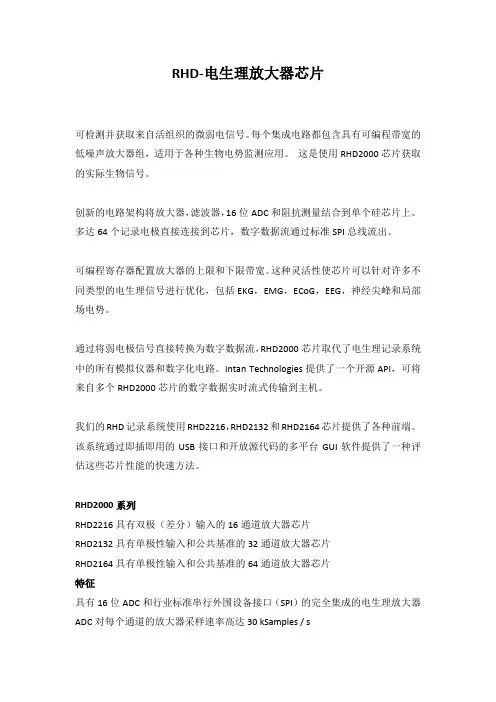
RHD-电生理放大器芯片可检测并获取来自活组织的微弱电信号。
每个集成电路都包含具有可编程带宽的低噪声放大器组,适用于各种生物电势监测应用。
这是使用RHD2000芯片获取的实际生物信号。
创新的电路架构将放大器,滤波器,16位ADC和阻抗测量结合到单个硅芯片上。
多达64个记录电极直接连接到芯片,数字数据流通过标准SPI总线流出。
可编程寄存器配置放大器的上限和下限带宽。
这种灵活性使芯片可以针对许多不同类型的电生理信号进行优化,包括EKG,EMG,ECoG,EEG,神经尖峰和局部场电势。
通过将弱电极信号直接转换为数字数据流,RHD2000芯片取代了电生理记录系统中的所有模拟仪器和数字化电路。
Intan Technologies提供了一个开源API,可将来自多个RHD2000芯片的数字数据实时流式传输到主机。
我们的RHD记录系统使用RHD2216,RHD2132和RHD2164芯片提供了各种前端。
该系统通过即插即用的USB接口和开放源代码的多平台GUI软件提供了一种评估这些芯片性能的快速方法。
RHD2000系列RHD2216具有双极(差分)输入的16通道放大器芯片RHD2132具有单极性输入和公共基准的32通道放大器芯片RHD2164具有单极性输入和公共基准的64通道放大器芯片特征具有16位ADC和行业标准串行外围设备接口(SPI)的完全集成的电生理放大器ADC对每个通道的放大器采样速率高达30 kSamples / s低本底噪声:典型值为2.4μVrmszui高截止频率可配置为100 Hz至20 kHz较低的截止频率可配置为0.1 Hz至500 Hz集成的多频原位电极阻抗测量功能辅助ADC输入,用于连接其他片外传感器应用领域用于神经记录的微型多通道探头大规模并行神经记录,用于高级大脑活动映射用于电生理实验的低功率无线讲台或背包“智能培养皿”体外记录系统同时记录微电极的动作电位和局部场电位(LFP)便携式多通道EKG或EMG监控系统先进的假肢控制器前端。
Zonghe Yanjiu♦综合研究|经颅聚焦超声技术在神经外科中的应用与研究进展庄晓鹏刘佳运(广东工业大学,广东广州510006)摘要:对国内外经颅聚焦超声技术的最新进展进行综述,介绍了在经颅聚焦超声中常用的换能器类型、刺激参数与超声作用机理,并对经颅聚焦超声在神经外科中的应用进行了分析,探讨了未来可能的研究方向。
关键词:经颅聚焦超声;超声换能器;神经外科0引言大脑是一个结构和功能复杂的系统,大脑区域的细胞结构和。
脑的往往与大脑的异常放电、神经元丢或神经的有。
神经与刺激是的方,可脑作并。
常神经调节与刺激方脑电刺激(DCS)、经颅磁刺激(TMS)和经颅直流电刺激(tDCS)。
对于DCS,其需要进行神经外科手术将刺激器脑内,可能术并,刺激焦,了技术在神经外科域的进一应用。
TMS电应理,的能在大脑内应电流,使大脑中的神经元或轴突去tDCS的电电,电进入大脑,是TMS是-DCS,在大脑中的电是分,对大脑作用,现紧密的聚焦和对脑核团的刺激。
经颅聚焦超声因其无创伤、可对脑深部核团进行特异性刺激和双向可逆神经的特点,得到了广泛的关注。
目前,国内外己经开展多项动验和临床研究来证明该技术的性和安全性。
本文总结了在经颅聚焦超声中常用的超声换能器、刺激参数与作用机理,并对经颅聚焦超声在神经外科中的应用进行了研究。
1超声换能器常用于经颅聚焦超声的换能器主要有单阵元聚焦换能器、阵列换能器和声全息透镜。
Samoudi等人了下丘脑区域的神经元活动,根据聚焦的深度和神经核团的大小,设计了一种单阵元聚焦换能器,相较于阵列换能器,对驱动电求,控电简单,成本低[1],该换能器现焦斑的电子转向和控,只能通过机械扫描的方式进行扫描移动。
同时,由于只一个阵元,所相控聚焦的方式补偿颅骨和软组织的相位畸变,进影响果。
Yang等人了实现更好的电子聚焦和更大的偏转角度,开发了一种可用于非人灵长类经颅聚焦超声的可扩展二维平面阵列凹。
Chaplin等人设计了一种磁共系统兼容的聚焦机阵列换能器,用向刺激的S1区域),在中,可通过磁共振成像系统进行监测和引导。
相控阵扫描时增益下降公式英文回答:When a phased array is scanned, the gain of the array decreases. This is because the energy from the individual elements is no longer focused in the same direction. The amount of gain loss depends on the scan angle and the number of elements in the array.The gain loss due to scanning can be calculated using the following formula:Gain loss = 10 log(1 (sin(θ/2)/sin(θ))^N)。
where:θ is the scan angle.N is the number of elements in the array.For example, a 16-element phased array will have a gain loss of 0.5 dB when scanned to 30 degrees.The gain loss due to scanning can be compensated for by increasing the power of the individual elements. However, this can lead to increased power consumption and heat dissipation.中文回答:当相控阵扫描时,阵列的增益会下降。
这是因为各个单元格的能量不再聚焦在同一个方向上。
增益损失量取决于扫描角度和阵列中单元格的数量。
由于扫描造成的增益损失可以用以下公式计算:增益损失= 10 log(1 (sin(θ/2)/sin(θ))^N)。
radar 术语全文共四篇示例,供读者参考第一篇示例:雷达是目前在军事和民用领域广泛使用的一种探测和跟踪目标的技术。
它通过向目标发射电磁波并接收目标反射的波来确定目标的位置、速度和其他相关信息。
雷达术语是在雷达领域常用的术语,了解这些术语对于理解雷达技术和运作原理至关重要。
1. 雷达系统:雷达系统是由雷达发射器、接收器、天线和信号处理器等组件组成的系统。
它们一起工作来探测和跟踪目标,并将信息传递给操作员或自动控制系统。
2. 发射器:雷达系统中的发射器用于发射电磁波信号。
这些信号通过天线发送到目标,并在目标上产生反射。
3. 接收器:雷达系统中的接收器用于接收从目标反射回来的电磁波信号。
接收器将这些信号转换成可供处理的数据。
4. 天线:雷达系统中的天线用于发射和接收电磁波信号。
天线的设计对雷达系统的性能有着重要影响。
6. 工作模式:雷达系统可以处于不同的工作模式,包括搜索模式和跟踪模式。
搜索模式用于在广阔范围内搜索目标,而跟踪模式用于精确跟踪已发现的目标。
7. 极坐标:雷达系统中常用的坐标系,用于描述目标的位置和距离。
极坐标通常由方位角和仰角组成。
8. 方位角:雷达系统中用于描述目标在水平方向上的位置的角度。
方位角通常从雷达系统正前方开始计算。
10. 系统灵敏度:雷达系统的灵敏度指的是系统能够检测到的最小信号强度。
灵敏度越高,系统可以探测到更小的目标。
11. 脉冲宽度:雷达系统发射的脉冲信号的宽度。
脉冲宽度影响雷达系统对目标的分辨能力。
13. 探测范围:雷达系统可以检测到目标的最大距离。
探测范围受到雷达系统功率、天线性能和目标反射特性的影响。
15. 杂波抑制:雷达系统通过对接收信号进行处理来抑制杂波的干扰。
杂波抑制能力影响雷达系统的性能和准确性。
16. 脉冲压缩:雷达系统通过脉冲压缩技术可以提高雷达系统的分辨率和目标跟踪能力。
17. 后向散射截面:后向散射截面是描述目标对雷达系统反射效果的物理量,它影响雷达系统对目标的探测和跟踪能力。
一种小规模超宽带相控阵天线设计柏艳英【摘要】目前基于阵元间强耦合效应已设计出超宽带相控阵天线,但是其规模较大.针对规模小或者在扫描方向上规模小,如何增强阵元间耦合而实现超宽带相控阵天线的问题,采用平衡对踵Vivaldi天线(BAVA)作为天线单元,优化天线单元辐射金属的形状,并采用镜像法布阵天线单元设计出一个小规模4×16的斜极化超宽带相控阵天线.仿真和试验结果表明,采用的方法可以增强小规模超宽带相控阵天线的阵元间耦合效应,实现频率0.8f0~2.0f0(f0为工作频率)驻波比小于2,法向增益达17.34~23.0 dBi,在±45°范围内实现无栅瓣扫描.该小规模超宽带相控阵天线已在实际工程中应用.%At present,a lot of ultra-wideband(UWB) phased arrays have been designed based on the strong mutual coupling between the array elements.But the UWB phased arrays are large.For a small scale or a small scale array in the scanning direction,the problem of how to achieve the ultra-wideband perform-ances by enhancing the mutual coupling between the array elements is necessary to be developed.In this paper,Balanced Antipodal Vivaldi Antennas (BAVAs) are adopted. By optimizing the radiation metal shape and arranging the direction of the antenna elements with mirroring technique,a small 4×16 oblique polarization UWB phased array is designed.The simulation and experiment results show that this method can enhance the mutual coupling between the small UWB array elements. The array has a good voltage standing-wave ratio(VSWR) less than 2.0 in the frequency 0.8f0~2.0f0(f0is the operation frequency), norm gain 17.34 ~23.0 dBi,and large scanning angle beyond 45° without gratinglobes. The designed small scale UWB phased array antenna has been applied in engineering.【期刊名称】《电讯技术》【年(卷),期】2018(058)002【总页数】5页(P214-218)【关键词】超宽带相控阵天线;平衡对踵Vivaldi天线(BAVA);阵元耦合;镜像技术;大角度扫描【作者】柏艳英【作者单位】中国西南电子技术研究所,成都610036【正文语种】中文【中图分类】TN822.81 引言超宽带相控阵天线是天线综合技术发展的一个重要方向,有利于满足成本、尺寸、重量、性能要求,减少传感器综合的天线总数,实现天线资源的高度综合和高效共享。
2ˑ2phased array consisting of square loop antennas for high gain wide angle scanning with low grating lobes [J].IEEE Transactions on Microwave Theory and Tech-niques,2017,65(2):576-583.[4]㊀WEN Y Q,WANG B Z,DING X.A wide -angle scanning and low sidelobe level microstrip phased array based on genetic algorithm optimization[J].IEEE Transactions on Antennas and Propagation,2016,64(2):805-810.[5]㊀MAILLOUX R J.Phased array antenna handbook[M].2nd ed.New York:Artech,2008.[6]㊀薛永,栾珊,王晓婷,等.相控阵天线在通信卫星中的应用分析[C]//中国飞行器测控学术年会论文集.北京:清华大学出版社,2018:20-29.[7]㊀朱文冰.星载合成孔径雷达的可靠性设计[J].现代雷达,2006,28(4):75-78.[8]㊀侯雪风,祝大龙,刘德喜,等.用于星际数传的S 波段四通道T 组件[J].遥测遥控,2018,39(3):43-47.[9]㊀KROENING A M.Advances in ferrite redundancy switc-hing for Ka -band receiver applications[J].IEEE Trans-actions on Microwave Theory and Techniques,2016,64(6):1911-1917.[10]㊀SINHA S,BANSA1D,RANGRA K J.RF MEMS com-pact t -type switch design for switch matrix applications in space telecommunication[C]//Proceedings of ICAE-SM -2012.Nagapattin:IEEE,2012:130-135.[11]㊀ZAHR1A H,ZHANG L Y,DORION C,et al.Long -term actuation demonstration of RF -MEMS switches for spaceapplications [C]//Proceedings of 2018Symposium on Design,Test,Integration and Packaging of MEMS and MOEMS.Roman:IEEE,2018:130-135.[12]㊀龚秀丽,孙绍强,李鑫.射频开关在高低温电测试试验中的失效分析及改进[J].电子设计工程,2016,24(23):115-121.[13]㊀严丰庆,钱澄.射频开关及其在通信系统中的应用[J].电子器件,2005,28(1):97-100.[14]㊀张凯,延波,徐锐敏.Ka 频段上变频模块的设计[J].电讯技术,2007,47(5):100-103.[15]㊀陈红卫.双频和3-6GHz 宽带功分器及其小型化研究与设计[D].昆明:云南大学,2015.[16]㊀SHI J,QIANG J,XU K,et al.A balanced branch -line coupler with arbitrary power division ratio [J ].IEEE Transactions on Microwave Theory and Techniques,2017,65(1):IEEE,2018:78-85.[17]㊀李东亚,薛红喜.新型3dB 电桥的设计[J].电讯技术,2009,49(11):90-93.[18]㊀POZAR D M.微波工程[M].张肇仪,周乐柱,吴德明,等译.3版.北京:电子工业出版社,2006.作者简介:姚亚利㊀女,1989年生于河南洛阳,2017年获博士学位,现为工程师,主要研究方向为相控阵天线㊂简讯‘电讯技术“继续入选中国科技核心期刊2020年12月29日,中国科学技术信息研究所(简称中信所)以在线会议方式召开 2020年中国科技论文统计结果发布会 ,发布了‘2020年版中国科技期刊引证报告(核心版)自然科学卷“㊂根据该报告,‘电讯技术“继续被收录为 中国科技核心期刊 (中国科技论文统计源期刊),且核心总被引频次㊁核心影响因子和综合评价总分等关键指标明显提升㊂‘2020年版中国科技核心期刊引证报告(核心版)自然科学卷“以‘中国科技论文与引文数据库(CST-PCD)“为基础,采用科学客观的研究方法与评价方式,通过定量评价与专家评审,遴选出了中国自然科学领域各个学科分类的重要期刊作为统计来源期刊㊂该卷收录了在中国(不含港澳台地区)正式出版的1949种中文期刊和121种英文期刊,共2070种 中国科技核心期刊 ㊂与2019年版相比,总量增加了21种,有26种中文期刊和10种英文期刊新入选,部分期刊因不符合学术质量和水平要求以及存在违规和学术不端行为被淘汰,体现了科技核心期刊的继承性与动态性㊂中信所的科技核心期刊遴选每年一次,选出的中国科技核心期刊是中国各学科领域中较重要的㊁能反映本学科发展水平的科技期刊,相关成果被科技管理部门和学术界广泛应用㊂四川省有87种自然科学类期刊入选,中国电子科技集团有限公司(中国电科)有17种期刊名列其中㊂本刊编辑部㊀赵勇㊃14㊃第61卷姚亚利:高可靠低功耗Ka 频段星载有源相控阵冗余备份技术第1期。
美军雷达命名规范按老美军用标准MIL-STD-196D规定,其军用电子设备(包括雷达)根据联合电子类型命名系统(JETDS)。
名称由字母AN(陆军-海军联合命名系统),一条斜线和另外三个字母组成。
三个字母表示设备安装位置,设备类型和设备用途。
比如AN/SPS-49表示舰载警戒雷达。
数字49标识特定装备,并且表示该设备时JETDS规定的SPS类的第49种。
经过一次修改F 地面固定G 地面通用K 水陆两用M 地面移动式U 通用V 地面车载W 水面或水下Z 有人和无人驾驶空中备C 载波设备D 放射性检测,指示,计算设备E 激光设备G 电报,电传设备I 内部通信和有线广播J 机电设备T 电话(有线)设备V 目视和可见光设备W 武器特有设备X 传真和电视设备H 记录K 计算M 维修或测试工具N 导航(测高,信标,有源滤波器Active filter有源校正网络Active corrective network有源干扰Active jamming 机载引导雷达Airborne director radar机载动目标显示 Airborne MTI机载雷达 Airborne radar机载截击雷达Airborne-intercept radar机载警戒雷达Airborne warning radar模拟信号 Analog signal战场侦察雷达 Battle-field search radar 盲区 Blind zone闪烁干扰 Blinking jamming击穿功率 Breakdown power 体效应二极管本地振荡器Bulk effect diode local oscillator宽带中频放大器Broad band intermediate frequency amplifier 机柜、分机结构Cabinet,器信道化接收机 Channelized receiver 圆极化平面波 Circularly polarized plane wave闭环控制系统(反馈控制系统)Close-loop control system (feed-back control system)杂波抑制 Clutter suppression同轴电缆 Coaxial cable 同轴谐振腔 Coaxial cavity连续波雷达接收机 Continuous-wave radar receiver对比度Contrast 卷积器Convolutor 变频损耗 Conversion loss 相关时间Correlation time抗反辐射导弹措施Counter anti-radiation missile measures正交场器件(M型器件)截数据处理 Data processing偏转线圈 Deflection coil延时充电电路Delayed charging circuit介质移相器Dielectric phase shifter介质干扰杆 Dielectric chaff rod数字滤波器 Digital filterE面(H面)折叠双T E plane (H plane) magic-T天线的有效面积 Effective area of an antenna电液伺服阀Electro-hydraulic Servo value电磁兼容性Electromagnetic compatibility电子抗干扰Electronic anti-jamming)radar快速付里叶变换Fast Fourier Transform馈电网络 Feed network 相控阵馈电网络Feed networks For Phased Array铁氧体移相器Ferrite phase shifter火控雷达 Fire control radar 频率炮瞄雷达 Gun directing radar 回旋管 Gyrotron测高雷达 Height-finding radar水平极化场矢量Horizontally polarized field vector喇叭天线 Horn antenna 环行电桥Hybrid ring液压泵 Hydraulic pumpa干扰调制样式 Jamming modulation type干扰信号带宽 Jamming signal band width速调管 Klystron激光雷达Laser radar 线阵天线Linear array antenna 负载阻抗Load impedance低空搜索雷达Low altitude微波带通滤波器Microwave band-pass filter微波场效应晶体管放大器 Microwave field effect transistor amplifier 微波全息雷达 Microwave hologram radar微波低通滤波器 Microwave low-pass filter副瓣电平 Minor (side) lobe level归一化差斜率Normalized difference slope单通道单脉冲雷达One-channel Monopulse Radar开环系统频率特性 Open-loop system frequency characteristic运算放大器 Operational Amplifier 超视距雷达 Over-the-horizon radar脉冲压缩雷达Pulse compression radar 脉冲雷达接收机 Pulse radar receiver相控阵的量化误差Quantization error of a phased array雷达精度 Radar accuracy 雷达反侦察 Radar anti-reconnaissance天线罩 Radome达三通道单脉冲雷达接收机Three-channel monopulse radar receiverT型(Y型)环行器(结环行器) T-type (Y-type) circulator (junctioncirculator)静电控制超高频电子管(栅控管) UHF electronstatic control tubeV形波束雷达 V-beam radar 座 X-Y type antenna pedestal八木天线 Yagi antenna雷达覆盖范围Zone of radar coverage。
联发科技,在大陆地区被习惯称呼为“联发科”,是著名IC设计生产厂商,专注于无线通讯及数字多媒体等技术领联发科的MT6575 Android平台嵌入式芯片域。
其提供的芯片整合系统解决方案,包含无线通讯、高清数字电视、光储存、DVD及蓝光等相关光电产品领域。
联发科技成立于1997 年,已在台湾证券交易所公开上市,股票代号为2454。
总部设于台湾,并设有销售或研发团队于中国大陆、印度、美国、日本、韩国、新加坡、丹麦、英国及迪拜等国家。
[1]联发科技提供创新的芯片系统整合解决方案,包括光储存、数字家庭(含高清数字电视、DVD播放器及蓝光播放器)及移动通讯等产品,为全球唯一提供IC解决方案横跨资讯科技(IT)、消费性电子及无线通讯领域的IC设计公司,同时也是全球IC设计公司前十名中唯一的亚洲公司。
联发科技致力提供高性能及稳定的芯片解决方案予客户,透过高度整合及深度定制化,不仅提供客户差异化空间、亦可大幅缩短产品上市时间,并与客户一起打造更好的用户体验。
自2006年起联发科技投入大量资源于「精品计划」,致力提供全球客户高整合、低功耗的高性能手机解决方案。
藉由多项硬件测试,与客户一起努力将消费者最关心的如通话/收讯质量、待机时间等项目质量共同开发臻世界水平。
编辑本段发展历史2012年2012年6月22日联发科与晨星宣布了合并的计划,根据双方的公开讯息,联发科将公开收购晨星股权,公开收购案将分2阶段进行,预定收购晨星40%至48%股权。
[2]2011年●荣获2011年度《电子设计技术》通信与网络“优秀产品奖”●荣获2011年度《通信世界》中国通信业年度龙虎榜“技术创新大奖-芯片创新奖”●荣获2011年度《电子产品世界》编辑推荐奖“最佳手机/便携处理平台”●荣获印度"多媒体通信基础设施协会"(CMAI Association of India)颁发 2011年第五届国家电信奖- “最佳移动电话技术“●荣获英国《金融时报》评选之“最具勇气企业奖”●荣获《中国电子报》颁发 "2010年度最受中国市场欢迎的半导体品牌"●2011年3月16日,联发科(MTK)通过换股并购Ralink雷凌公司,将Ralink 作为联发科旗下的无线技术事业群,2011年10月1日并购正式生效●2011年 5篇ISSCC 论文发表, 刷新国内产业界论文发表记录——- An Injection-Locked Ring PLL with Self-Aligned Injection Window- A 70Mb/s -100.5dBm Sensitivity 65nm lP MIMO Chipset for WiMaX Portable Router (Industrial Demo)- A Saw-Less GSM/GPRS/EDGE Receiver Embedded in a 65nm CMOS Soc (Industrial Demo)- A Receiver for WCDMA/EDGE Mobile Phones with Inductorless Front-End in 65nm CMOS- A GPS/Galileo Soc with Adaptive in-Band Blocker Cancellation in 65nm CMOS2010年●2010年12月成立联发科软件(武汉)有限公司手机单芯片解决方案荣获《EDN China 2010 年度创新奖》颁发“最佳通信产品奖”获《华尔街日报》评选为“2010年度亚洲最受尊敬企业200强”Top 10●2010年9月成立联发芯软件设计(成都)有限公司获美国《商业周刊》评选为世界科技100强第12名●获世界杰出华商协会评选为“2010全球最具成长性的华商上市公司”荣获WAPI产业联盟颁发“WAPI芯片贡献奖”ISSCC 论文发表--「23.6 A 1V 17.9dBm 60GHz Power Amplifier in Standard 65nm CMOS」及「11.3 A SiGe BiCMOS 16-Element Phased-Array Transmitter for 60GHz Communications」荣获TD-SCDMA产业联盟(TDiA)颁发TD芯片技术创新奖2009年●荣获2009年度科学工业园区创新产品奖 (High Sensitivity GPS SOC)手机单芯片解决方案荣获《通信产业报》颁发“编辑选择奖”荣获《通信产业报》评选为最佳终端芯片平台获《手机圈》传媒选为2009中国手机芯片企业金品奖十佳●( Global Semiconductor AllianceGSA20091. A Multi-Format Blu-ray Player SoC in 90nm CMOS2. A 1.2V 2MHz BW 0.084mm2 CT ΔΣADC with -97.7dBc THD and 80dB DR Using Low-Latency DEM3. A 250Mb/s-to-3.4Gb/s HDMI Receiver with Adaptive Loop Updating Frequencies and an Adaptive Equalizer4. A 110nm RFCMOS GPS SoC with 34mW -165dBm Tracking Sensitivity●荣获赛迪顾问评为"2009中国3G产业芯片领域最具竞争力企业” 获《天下杂志》评为第二届“天下企业公民TOP 50"2008年●连续第三年获全球半导体联盟 ( Global Semiconductor Alliance;GSA)选为2008“最佳财务管理的IC设计公司”●《天下杂志》评为第二届“天下企业公民TOP 50”●《远见杂志》评为第四届“远见企业社会责任奖”●首创台湾科技公司连续五年发表于IEEE ISSCC纪录——“A 1V 11b 200MS/s Pipelined ADC with Digital Background Calibration in 65nm CMOS”和“A F ractional Spur Free All-Digital PLL with Loop Gain Calibration and Phase Noise Cancellation for GSM/GPRS/EDGE”●荣获赛迪顾问评为"2008年中国手机芯片市场-成功企业" 荣获《中国电子报》选为 "2008年度最受中国市场欢迎的半导体品牌" 获世界杰出华商协会评选为2008全球华商高科技500强荣获2008年度科学工业园区创新产品奖(Full HD ATSC iDTV SOC)2007年●连续第二年获IC设计产业协会( Fabless Semiconductor Association;FSA)选为2007「最佳财务管理的IC设计公司」●ISSCC论文发表--「A 1V 11b 200MS/s Pipelined ADC with Digital Background Calibration in 65nm CMOS」和「A Fractional Spur Free All-Digital PLL with Loop Gain Calibration and Phase Noise Cancellation for GSM/GPRS/EDGE」(创台湾科技公司首位连续五年,共计七篇论文获选发表的纪录,也是今年台湾唯一入选的业界代表)●IEEE IRPS (International Reliability Physics Symposium)论文发表--「A new device reliability evaluation method for overdrive voltage circuit application」●获《Forbes Asia》杂志列为《亚洲企业50强》之一●获第十五届《经济部产业科技发展奖》之”卓越创新成就奖”●获《天下杂志》评为第十二届“台湾最佳声望标竿企业”●获《远见杂志》评为第三届“远见企业社会责任奖”●获《天下杂志》评为第一届“天下企业公民TOP 50”2006年●获IC设计产业协会( Fabless Semiconductor Association;FSA)选为2006「最佳财务管理的IC设计公司」●荣获2006年度科学工业园区创新产品奖( Blu-ray晶片组)●获《Forbes Asia》杂志列为《亚洲企业50强》之一●推出DTV数位电视晶片、Blu-ray晶片●ISSCC论文发表--Fully Integrated CMOS SoC for 56/18/16 CD/DVD-dual/RAM Applications●HDTV-reading SOC, Super-multi SOC●荣获2005年科学工业园区创新产品奖(Multimedia GSM/GPRS Mobile Phone Chipset)●ISSCC论文发表--Multi-Format Read/Write SoC for 7x Blu-ray/16xDVD/56xCD DLL-Based Clock Recovery In a PRML Channel●获《Forbes Asia》杂志列为《亚洲企业50强》之一●获《天下杂志》评为第十届“台湾最佳声望标竿企业”2004年●荣获2004年科学工业园区创新产品奖(DVD-Recorder Backend单晶片)●获Euromoney 04年全球最佳治理典范企业调查,排名居台湾地区高科技企业第三名●ISSCC论文发表--Combo Driver Applications●获《天下杂志》评为第九届“台湾最佳声望标竿企业”2003年●荣获2003年科学工业园区创新产品奖(8倍速DVD dual复写型光碟机晶片组) ●荣获第15届行政院国家品质奖●推出DVD-Dual晶片组●获选“数位时代双周刊”台湾科技100强第一2002年●荣获2002年科学工业园区创新产品奖(高倍数COMBI复合型光碟机晶片组) ●推出48XCD-RW晶片组●推出COMBI晶片组2001年●荣获2001年度科学工业园区创新产品奖(高整合度DVD-Player晶片组)●荣获第9届经济部产业科技发展奖之卓越成就奖●于台湾证券交易所正式挂牌上市,股票代号24542000年●荣获2000年科学工业园区创新产品奖(12/8/40倍数CD-R/RW晶片组)●推出12XCD-R/RW晶片组1999年●荣获1999年科学工业园区创新产品奖(12倍速DVD-ROM晶片组)●推出12X DVD-ROM晶片组●荣获1998年科学工业园区创新产品奖(CD-ROM Digital data/servo processor 产品)●推出全球最快速的48X CD-ROM晶片组1997年●五月公司成立编辑本段业务领域光储存领域◆光储存领域,联发科技领先全球推出包含CD-ROM、DVD-ROM、DVD-Player、CD-R/RW、Combi、DVD-RW等相关控制芯片组。
毕业设计(论文)外文文献翻译翻译(1)题目相控阵和雷达技术的突破翻译(2)题目发射KU-波段的相控阵天线在FSS通信系统中的应用学院电子信息学院专业英文译文1:相控阵和雷达技术的突破【摘要】许多人认为雷达是一个成熟的领域,不会发生任何新的变化,这种看法存在很久了,没有比这个看法更错误的了。
当我1950年参与到雷达领域的时候,我也有过同样的看法,例如,我认为麻省理工学院的雷达丛书已经是包罗万象了,不需要增加任何新的内容。
然而我是多么的错啊,从那时起雷达技术领域中已经发生了许多令人眼花缭乱的发展,雷达一直受益于Moore s定律和许多新的技术上的成果,例如,MMIC GaAs T/R组件和相控阵组件。
现在雷达技术发展得更快了,在这篇文章里,我将给出某些最近突破的例子。
【关键词】雷达;有源相控阵;MMIC;MEMS;T/R组件;相控阵;AESA;电扫;GaAs;GaN;SiC;CMOS;数字波束形成;自适应阵列;旁瓣对消器;超宽带天线;金属材料;电子管;真空电子器件;回旋管;磁控管;速调管;行波管;微波功率组件;MPM;功率放大组件;SBX;GBR—P0:SEA-BASED X-波段雷达24层楼高的SEA-BASED X-波段相控阵雷达是一个世界奇迹。
1:GaAs MMIC T/R模块(单片微波集成电路)在过去的十年成功和广泛的应用了MMIC和AESA(有源电子扫描阵)2:低成本¥19K AESA谁说AESA是非常昂贵的,在DARPA(Defense Advanced Research Projects Agency美国国防部先进研究项目局)的低资金¥19K资助下使35GHZ相控阵成为可能。
DARPA 已经资助发展了¥10 X-band,10’smW,单T/R芯片模块。
3:低成本的MEMS(微机电系统)相控阵即使我们只有一个低损耗的移相器,那么就能够用在一个模块上安装很多的移相而MEMS提供了这个可能。
p channel fet p 沟道场效应晶体管p channel metal oxide semiconductor transistor p 沟道金属氧化物半导体晶体管p channel mos p 型沟道金属氧化物半导体p contact p 型接触p diffused region p 型扩散区p dopant p 型掺杂剂p dopant modifier p 型掺杂剂p doped drain p 型掺杂漏极p doped semiconductor p 型半导体p doped source p 型掺杂源极p epi p 型外延层p i n diode pin二极管p i n diode phase shifter p i n 二极管移相器p i n photodiode p i n 光电二极管p n junction p n 结p n junction isolation p n 结隔离p n junction rectification p n 结型整流p type conduction p 型导电性p type diffusion p 型扩散p type dopant p 型掺杂剂p type doping p 型掺杂p type semiconductor p 型半导体p well diffusion p 阱形成扩散p well mask p 阱形成掩膜p+ guard ring p+ 型保护环pack 部件pack carrier television station 便携式电视发射机package 外壳package assembly 外壳组装package base 外壳基座package closure 管壳密封package header 外壳基座package inductance 管壳电感package lead 外壳引线packaged chip 封装的集成电路packaged integrated circuit 封装的集成电路packaged tube 成套管packageless integrated microcircuit 无封装集成微型电路packaging 封装packaging density 组装密度packaging hardware 封装装置packaging socket 封装用底座packaging system 封装装置packet 包packet communication 包通信packet network 包交换网络packet switched network 包交换网络packet switching 包交换packet transmission 包传输packet transmission system 包传输系统packing 包装packing density 组装密度pad 焊径pad layer 焊接层pad registration 焊接点重合pager 页面等程序pair 电偶pair creation 电子空穴对产生pair production 电子空穴对产生paired echo 对回波pal 可编程序逻辑阵列palladium silver conductor system 钯银导体系统pam 脉冲幅度灯pancake package 偏平管壳panel 板panel mounting 面板装配panelectronics 泛电子学panoramic receiver 扫涤收机pantelegraphy 传真电报学pantograph 比例画器parabolic index optical fiber 抛物线折射率剖面光纤维parabolic mirror 抛物柱面镜parabolic reflector 抛物面反射器parabolic reflector antenna 抛物面反射体天线parabolically graded optical fiber 抛物线折射率剖面光纤维paracrystal 不完全晶体parallel beam 平行光束parallel feed 井联馈电parallel gap weld 平行间隙式焊接parallel interface 并行接口parallel light beam 平行光束parallel mirror cavity 平行镜空腔parallel operation 并行操作parallel plate electron multiplier 平行板电极式电子倍增管parallel plate plasma etcher 平行板等离子体腐蚀装置parallel resonance 并联谐振parallel transfer ccd 并行转移电荷耦合掐parametric amplification 参量放大parametric amplifier 参量放大器parametric gain 参量放大parametric interaction 参数相互酌parametric laser 参量激光器parametric oscillator 参量振荡器parametric pumping 参数抽运parametric resonance 参量谐振paraphase amplifier 倒相放大器parasite frequency modulation 寄生档parasitic action 寄生酌parasitic capacitance 寄生电容parasitic element 寄生元件parasitic oscillation 寄生振荡parasitic oscillation suppression 寄生振荡抑制parasitic oscillations 寄生振荡parent material 母体材料part 元件part reliability 部件可靠性partial compatibility 部分兼容性partial dislocation 局部位错partial pressure 分压partial pressure analyzer 分压分析器partial pressure gage 分压分析器partially reflecting mirror 部分反射镜partially transparent mirror 部分透玫particle 粒子particle accelerator 粒子加速器particle beam technology 粒子束技术particle bunching 粒子聚束particles flux 粒子流particles separation 粒子分离particles storage 粒子存储particulate contamination 微粒子污染parts per billion 十亿分之几parts per million 百万分之parts per trillion 兆分之party 群party line 合用线party line system 同线电话制passband 通频带passivant 钝化剂passivated surface 钝化表面passivating coating 钝化涂层passivating layer 钝化层passivation 钝化passivation etching 钝化层腐蚀passive antenna 无源天线passive component 无源元件passive element 无源元件passive homing 被动导航passive isolation 钝态隔离passive q switch 无源 q 开关passive q switching 无源祋passive repeater 无源中继器passive retransmission 无源转播passive satellite repeater 无源卫星转发器passively mode locked laser 无源锁模激光器paste composition 膏成分paste system 膏系统path 路程path length 路程长度path loss 路径损耗path of propagation 传播路径pattern 光栅;图样pattern alignment 图形对准pattern array 图像阵列pattern blurring 图像模糊pattern definition 图案形成pattern element 图形单元pattern fabrication 图像形成pattern formation 图形生成pattern generation 图形生成pattern generator 测视图案信号发生器;图形发生器pattern identification 图形识别pattern mask 图像掩模pattern matrix 图像阵列pattern repeater 步进重复照相设备pattern replication 图像重复pattern writer 绘图机patterned film 有图膜patterning 图案形成patterning exposure 图像形成曝光pbx 专用小交换机pc 印刷电路板pcb 印刷电路板pcb insertion 印刷电路板装配pci 多晶硅隔离pcm 脉码灯pcm exchange 脉码灯电话交换局pcm signal 脉码灯信号pdm 脉冲持续时间灯pdp 等离子体显示板peak 最大值peak current density 最大电淋度peak factor 峰值因数peak output power 最大输出功率peak power density 峰值功率密度peak power output adjustment 最大输出功率蝶peak pulse amplitude 峰值脉冲振幅peak sideband power 峰值边带功率peak signal 峰值信号peaker 微分电路pedestal chip 凸点焊盘型芯片pel 像素pellet part 片状掐pellicle 薄膜pellicle reticle 薄膜中间掩模peltier effect cooler 珀耳帖效应冷却器pencil beam antenna 锐锥形射束天线pencil tube 笔形管penetrability 穿透能力penetrating power 穿透能力peniotron 超高频放大管penning discharge 潘宁放电pentagrid 五栅管pentagrid converter 五栅管混频器五栅管变频器pentode 五极管penumbral blur 图像贸交界处模糊per amplifier 前置放大器per slice yield 薄片成品率per unit area concentration 单位面积浓度per unit volume concentration 单位体积浓度percentage modulation 灯度percentage modulation meter 灯度测试器perfect dislocation 完全位错perfect lattice 理想晶格performance 性能performance characteristic 动棕性performance monitor 性能监视器performeter 性能监视器periodic aerial 党驻波天线periodic antenna 党驻波天线periodic waveguide 周期性波导管peripheral blade 外圆型刀片peripheral chip 周边集成电路peripheral circuit 周边集成电路peripheral device 外围掐peripheral electron 外层电子peripheral saw 外圆型锯片permanent echo 固定目标的回波permanent mask 固定掩模permanent memory 固定存储器permanent storage 9 固定存储器permatron 磁场控制管permeability 导磁率permeability tuning 异磁系数党permeable base 穿透性基极permeameter 磁导计permissible irradiation 允许照射permissible orbit 允许轨道permitted transition 容许跃迁permittivity 介电常数perpendicular magnetization 垂直磁化persistence 余辉时间persistence characteristic 余辉特性persistency 持续性persistent photoconductivity 残留光电导性person to person call 定人呼叫personal call 定人呼叫perturbation 干扰perveance 导电系数pfet p 沟道场效应晶体管pfm 脉冲频率灯pga 管脚阵列phantom circuit 约像电路phase 相位phase adjustment 相位蝶phase advancer 进相器phase angle 相位角phase angle meter 相位角计phase changer 变相器phase coincidence 相位重合phase comparator 相位比较器phase compensator 相位补偿器phase constant 波长常数phase control 色爹phase converter 相位变换器phase corrector 相位补偿器phase delay 相位滞后phase detector 鉴相器检相器phase detuning 相位失调phase deviation 相位偏移phase diagram 相图phase difference 相位差phase discriminator 鉴相器检相器phase distortion 相位失真phase distortion corrector 相位补偿器phase equality 同相位phase equalization 相位均衡phase equalizer 相位均衡器phase error 相位误差phase error correction 相位误差校正phase focusing 相位聚焦phase frequency distortion 相位频率失真phase front 相位波前phase inversion 倒相phase jitter 相位择动phase lag 相位滞后phase lock 锁柑phase locked loop 锁相环路phase locking 锁相phase locking technique 锁相技术phase mode locking 相位模式同步phase modulated signal 掂信号phase modulation 掂phase modulator 相位灯器phase of a charged particle 带电粒子相位phase oscillations 相位振荡phase plane 相位平面phase precorrection 相位预校正phase reference 相位基准phase response 相位响应phase sensitive detector 相敏检波器phase shift 移相phase shift keyed signal 相移键控信号phase shift keying 相移键控phase shifter 移相器phase spectrum 相位谱phase stability 相位稳定度phase stabilization 相位稳定phase synchronization 相位同步phase transition 相位跃迁phase uniformity 相位均匀性phase variation 相转变phase velocity 相位速度phased antenna array 相控天线阵phased array radar 相控天线阵雷达phaser 帧同步机phasing 相位蝶phasing line 定相线phasing signal 整相信号phasometer 相位计phenolic resin 酚醛尸phono cartridge 拾音颇座phonogram 话传电报phonograph 留声机phonon maser 声子微波激射器phosphor 荧光体phosphor doping 磷掺杂phosphor dot 荧光点phosphor screen 荧光屏phosphorous diffusion source 磷扩散源phosphorous doped oxide 掺磷氧化物phosphorous emitter 掺磷发射极phosphorous ion implant 磷离子注入phosphorous semiconductor 掺磷半导体phosphorus 磷phosphosilicate glass 磷硅酸玻璃photo artwork 光原图photo darlington 光电晶体管达林顿电路photo fet 光控场效应晶体管photo field effect transistor 光控场效应晶体管photo field emission 光场致发射photo tool 光掩膜photoacoustic effect 光声效应photoactive electrode 光敏电极photoanode 光电阳极photoblank 掩模底版photocapacitance 光电电容photocapacitant detector 光电电容检测器photocathode 光电阴极photocathode travelling wave tube 光电阴极行波管photocell 光电池photochemical deposition 光化学淀积photochemical effect 光化学效应photochemical vapor deposition oxide 光化学汽相淀积氧化物photocomposer 照相排字机photocomposition 照相排字photocomposition machine 照相排字机photoconductive cell 光敏电阻器photoconductive detector array 光电导探测企列photoconductive element 光电导元件photoconductive film 光导层photoconductive layer 光导层photoconductive target 光电导靶photoconductivity 光电导性photocoupled semiconductor device 光电耦合半导体掐photocoupler 光电耦合器photocoupling 光电耦合photocurrent 光电流photodeposition 光化学淀积photodetector 光检测器photodiode 光电二极管photodiode array 光电二极管阵列photodissociation 光致离解photodissociation laser 光致离解激光器photodissociative laser 光致离解激光器photoelastic effect 光弹效应photoelectret state 光驻极状态photoelectric 光电的photoelectric cartridge 光电式拾音头photoelectric cell 光电池photoelectric effect 光电效应photoelectric emission 光电发射photoelectric reader 光扫描器photoelectric receptor 光电接收机photoelectric scanner 光电扫描器photoelectric signal voltage 光电信号电压photoelectricity 光电;光电现象photoelectrochemical cell 光电化学电池photoelectrochemical etching 光电化学腐蚀photoelectron 光电子photoelectron spectroscopy 光电子光谱法photoelectronics 光电子学photoelectrophoretic image display device 光电泳图象显示掐photoelelectronic device 光电子掐photoelement 光电池photoeletric memory device 光电存储掐photoeletric storage device 光电存储掐photoemission 光电发射photoemission spectroscopy 光电子发射光谱学photoemissive cell 光电发射元件photoemitter 光致发射体photoemulsion 照相乳胶photoengraving 光刻蚀photoetching 光刻蚀photoexcitation 光激励photoferroelectric 光敏铁电体photoformer 阴极射线函数发性器;光电函数发生器photographic mask 光掩膜photoionization 光电离photoionization laser 光致电离激光器photolacquer mask 光致抗蚀剂掩模photolayer 光敏层photolithographic mask 光刻用掩模photolithographic resolution 光刻蚀清晰度photolithography 光刻法photoluminescence 光致发光photolysis 光分解photolytic reduction 光解还原photomagnetoelectric effect 光磁电效应photomask 光掩膜photomask copy 光掩模复印photomask damage 光掩模损伤photomask drawing 光掩模草图photomask inspection 光掩模检查photomask inspector 光掩模测试设备photomask pattern 光掩模图形photomask processor 光刻装置photomask resolution 光掩模清晰度photomask scrubber 光掩模洗涤器photomasking 光刻法photometer 光度计photomicrograph 显微照片photomicrography 显微照相术photomultiplier 光电倍增管photomultiplier tube 光电增倍管photomultiplier with discrete dynodes 分离电极式光电倍增管photon 光量子photon amplification 光子僚大photon counter 光子计数器photon detector 光子探测器photon echo 光量子回波photon engine 光子发动机photon preionization laser 光子预电离激光器photon pumping 光子抽运photopiezoelectric 光压电体photoplate 照相底版photoplotter 光电绘图仪photopotentiometer 光电位计photoprocessing 光刻法photoreader 光电读出器photoreceiver 光敏接收器photoreceptor 光传感器photoreduction 照相缩板photorelay 光控继电器photorepeater 照相复印机photoresist 光致抗蚀剂photoresist burnoff 等离子去胶photoresist coater 涂胶器photoresist controlled etch 光刻胶掩蔽控制腐蚀photoresist developer 光刻胶显影剂photoresist edge build up 硅片边缘上光刻胶的积累photoresist etching 光刻胶掩蔽腐蚀photoresist film 光刻胶膜photoresist integrity 光刻胶完整性photoresist lacquer 感光尸photoresist lift off 光刻胶剥离photoresist mask 光致抗蚀剂掩模photoresist mask pattern 光致抗蚀剂掩模图形photoresist masked etching 光刻胶掩蔽腐蚀photoresist masking 光刻胶掩蔽photoresist pattern delineation 光刻胶层图像形成photoresist process 光刻法photoresist spinner 旋转涂胶机photoresistor 光敏电阻器photoresponsive junction 光敏结photosensitive 光敏的photosensitive film 感光膜photosensitive layer 光敏层photosensitive semiconductor 光敏半导体photosensitivity 光敏度photosensor 光敏元件photosetting 照相排字photosurface 感光面phototelegram 传真电报phototelegraphic apparatus 传真电报机photothyristor 光电闸淋phototransistor 光电晶体管phototron 矩阵光电管phototube 光电管photovaristor 光变阻器photovoltage 光电压photovoltage cell 光电池photovoltaic cell 光电池photovoltaic effect 光生伏打效应photovoltaic energy conversion 光生伏打能量转换photovoltaic module 光生伏打组件photox 光化学汽相淀积氧化物physical circuit 实线线路physical sputtering 物理溅射physical vapor deposition 物理汽相淀积physisorption 物理吸着pick up coil 耦合线圈pick up tube 电视摄像管pickup 拾音器pickup arm 拾音欺pickup link transmitter 拾像中继发射机picosecond holography 微微秒全息照相术picosecond pulse 微微秒脉冲picosecond technique 微微秒技术pictorial wiring diagram 图示接线图picture 图像picture altitude 图像高度picture amplifier 图像信号放大器picture black 黑图像picture element 像素picture frequency 帧频picture monitor 图像监视器picture reproduction 图像重显picture resolution 图像清晰度picture sharphness 图像清晰度picture signal 图像信号picture telephone 电视电话picture transmission 视频传输picture transmitting 图像传送picture tube 显像管piece part 零件piezocrystal 压电晶体piezoelectric 压电体piezoelectric cartridge 压电式拾音头piezoelectric crystal 压电晶体piezoelectric loudspeaker 压电扬声器piezoelectric microphone 压电传声器piezoelectric receiver 压电晶体受话器piezoelectricity 压电现象piezoresonator 压电谐振器pigtail 抽头pillow distortion 枕形失真pilot channel 异频电路pilot frequency 异频pilot signal 监控信号pilot wire circuit 控制线电路pin 管脚pin assignment 引脚分配pin compatibility 管脚互换性pin configuration 引脚分配pin diode pin二极管pin grid array 管脚阵列pin grid array package 管脚阵列型管壳pin grid spacing 管脚间距pin in line package 管脚阵列型管壳pin jack 管脚插口pinch compression 等离子体压缩pinch discharge 箍缩放电pinch discharge pumped laser 箍缩放电抽运激光器pinch discharge pumping 箍缩放电抽运pinch effect discharge 箍缩效应放电pinch off 夹断pinch roller 压紧轮pinhole 针孔pinout 引脚分配pinpoint soldering 点焊pip 尖头信号pipe diffusion 沿位错线扩散pirani gage 皮喇尼真空计piston 活塞piston attenuator 活塞式衰减器pit 洞pitch 管脚间距pitch control 行距控制pitch of grooves 槽间距pitting 凹坑的形成pixel 像素placer 放置器planar air isolation 平面型空气隔离planar circuit 平面电路planar diode 平极型二板管planar dopant host 片状扩散源planar electrode 平面电极planar epitaxial diode 平面型外延二极管planar epitaxial technique 平面外延工艺planar epitaxial transistor 平面型外延晶体管planar integrated circuit 平面集成电路planar junction 平面结planar lightguide 平面光波导planar mounted integrated circuit 偏平封装集成电路planar oxidation 平面氧化planar package 平面管壳planar photodiode 平面型光敏二极管planar plasma etcher 平面式等离子体腐蚀器planar plasma reactor 平面式等离子体腐蚀器planar process 平面工艺planar processing approach 平面技术planar source 片状扩散源planar technique 平面技术planar transistor 平面晶体管planar wafer 平面薄片planarity 平面度planarization ring 整平环planarized structure 平面型结构plane aerial 平面形天线plane antenna 平面形天线plane of polarization 偏振面plane parallel cavity 平行平面空腔plane polarized light 平面偏振光plane polarized wave 平面偏振波plane position indicator 平面位置指示器plane reflector antenna 平面反射旗线plane sinusoidal wave 平面正弦波plane wave 平面波planetary fixture 行星型夹具plank's constant 普朗克常数planning 元件布置plant intercommunication 厂内通信plasma 等离子体plasma accelerator 等离子体加速器plasma anodization 等离子体阳极氧化plasma ashing 等离子灰化plasma balance 等离子体平衡plasma chemical vapor deposition 等离子体化学汽相淀积plasma cloud 等离子体云plasma column 等离子体柱plasma confinement 等离子体约束plasma desmear system 等离子清洁处理装置plasma display 等离子体显示器plasma display panel 等离子体显示板plasma etch cleaning 等离子腐蚀清洗plasma etch mask 等离子腐蚀用掩模plasma etcher 等离子体腐蚀器plasma etching 等离子腐蚀plasma frequency 等离子体频率plasma gun 等离子枪plasma heating 等离子体加热plasma isolation 等离子体隔离plasma jet 等离子体射流plasma laser 等离子体激光器plasma lifetime 等离子体寿命plasma oscillations 等离子体振荡plasma oxidation 等离子体氧化plasma panel 等离子体显示板plasma sheath 等离子壳层plasma spraying 等离子溅射plasma sputtering 等离子溅射plasma stripping 等离子去胶plasma waves 等离子体波plasmatron 等离子立生管plastic battery 塑料电池plastic bleed 塑料漏出plastic capsulation 塑料封装plastic carrier 塑料载体plastic deformation 塑性变形plastic device 塑料封装掐plastic dual in line package 塑料双列直插式外壳plastic encapsulated integrated circuit 塑料封装集成电路plastic encapsulation 塑料封装plastic film 塑料膜plastic packaged integrated circuit 塑料封装集成电路plastic packaging 塑料封装plasticizer 增塑剂plate 板plate characteristic 阳极特性plate current modulation 屏极电疗plate detection 阳极检波plate dissipation 屏极耗散plate efficiency 阳极效率plate load 屏极负载plate neutralization 阳极中和plate of a capacitor 电容颇板片plate resistance 阳极电阻plate terminal 阳极端子plate voltage 阳极电压plated circuit 印刷电路plated hole 金属化孔plated resist 电镀抗蚀层plated through hole 电镀的穿孔plating 喷镀plating bath 电镀槽platinum 铂playback 再现pleochroic dye 多色性染料pliotron 高度真空管pll 镇相回路plotter 绘图机plotting table 标绘板plug and socket 插头插座plug board 插接板plug connector 插塞式连接器plug in module 插件plug in package 插入式组件plumbicon 氧化铅光导摄象管pm 掂pmos transistor p 沟道金属氧化物半导体晶体管pockels cell 普克尔斯盒pockels effect 普克尔斯效应pockels effect light valve 普克尔斯效应光阀point 点point cathode 点状阴极point charge 点电荷point contact 点接触point contact diode 点接触二极管point contact junction 点接触结point contact transistor 点接触晶体管point defect 点缺陷point diode 点接触二极管point radiator 点状辐射体point to point circuit 点到点通信point to point communication 点到点通信point to point link 点到点通信point transistor 点接触晶体管polarity 极性polarization ellipse 偏振椭圆polarization error 极化误差polarization holography 偏振光全息照相术polarization plane 偏振面polarization rotation 偏振面旋转polarization vector 极化失量polarized beam 偏振波束polarized light 偏振光polarized wave 极化波pole tip 磁头尖polisher lapper 研磨抛光机polishing etchant 抛光用腐蚀剂pollution detection 污染探测poly plant 多晶硅制造装置poly reox 多晶硅再氧化poly semiconductor 多晶半导体poly squared cmos 双层多晶硅互补金属氧化物半导体polyatron 多阳极计数管polychip dip 多片双列直插式外壳polycide gate 多晶硅硅化物栅极polycrystal 多晶polycrystal isolation 多晶硅隔离polycrystalline deposition 多晶淀积polycrystalline ingot 多晶锭polycrystalline silicon gate mos 多晶硅栅金属氧化物半导体polycrystalline structure 多晶结构polyimide adhesive 聚酰亚胺粘合剂polyimide film 聚酰亚胺膜polymer adhesive 聚合物粘合剂polymer thick film 聚合物厚膜polymeric resist 聚合物光刻胶polymeric sealant 聚合物密封剂polymerized photoresist 聚合物光刻胶polyresistor 多晶硅电阻器polyrod antenna 介质天线polysilicon 多晶硅polysilicon backfill 多晶硅填充polysilicon boat 多晶硅小舟polysilicon diffusion equipment 多晶硅管扩散炉polysilicon fet 多晶硅场效应晶体管polysilicon filling 多晶硅填充polysilicon gate ccd 多晶硅栅电荷耦合掐polysilicon gate process 多晶硅栅工艺polysilicon on oxide region 氧化物层上多晶硅区polysilicon self aligned process 多晶硅自对准工艺pool cathode 液体阴极pool rectifier 液体阴极整流population difference 粒子数差population inversion 粒子数反转population inversion lifetime 粒子数反转寿命population lifetime 粒子数寿命population measurement 粒子数测量porous getter 多孔吸气剂porous silicon 多孔硅port radar 港口雷达portable 携带式的portable laser 便携式激光器portable set 便携式无线电机portable television receiver 便携式电视接收机portable television transmitter 便携式电视发射机portable transmitter 便携式发射机position 位置positioner 位置控制器positioning system 位置控制器positioning table 定位台positive 正的positive artwork 正象原图positive bias 正偏压positive carrier 正电荷载劣positive column 正电柱positive electron affinity 正电子亲合力positive emulsion 正性乳剂positive feedback 正反馈positive glow 阳辉光positive image 正象positive image material 正性光刻胶positive ion beam 正离子束positive modulation 正极性灯positive pattern 正象positive photoresist 正性光刻胶positive phototool 正像掩模positive picture 正像positive rays 阳极射线positive record 正像记录positive resist lithography 正性胶光刻positive sync pulse 正同步脉冲positive temperature coefficient of resistance 电阻的正温度系数positive transmission 正灯传送post acceleration 后加速post bake 后烘post deflection acceleration 后加速post seal visual 密封后肉眼检查post selection 后选择postdevelopment bake 显影后烘烤postexposure bake 曝光后烘烤potential 电势potential barrier 势垒potential drop 电压降potential pit 势阱potential well 势阱potentiometer 电位计potted circuit 密封电路potted electronic module 密封电子组件potted element 密封元件potting 密封potting resin 密封用尸power 功率power amplifier 功率放大器power apparatus 电源设备power consumption 能量消耗power conversion 能量变换power density 功率密度power detector 功率方向继电器power divider 功率分配器power gain 功率增益power induction 电力线感应power integrated circuit 功率集成电路power loss 功率损耗power modulation 功率灯power module 电源组power output 功率输出power output variation 输出功率变化power pack 电源组power rating 额定功率power semiconductor 功率半导体掐power splitter 功率分配器power stability 功率稳定性power supply 电源power supply of laser 激光歧源power supply unit 电源部分power transistor 功率晶体管ppb 十亿分之几ppm 百万分之ppr 正性光刻胶ppt 兆分之pre amplifier 前置放大器pre epitaxial growth 外延前生长pre etch hardbake 腐蚀前烤硬pre implantation 预注入preacceleration 预加速preaging 预老化prealigner 预对准器prealignment 预对准preamplification 前置放大preamplifier 前置放大器prebake 前烘precap visual 密封前肉眼检查precedence indicator 优先指示符precession of orbit 轨道进动precession time 进动时间precipitating crystallization 沉淀结晶化precipitation 沉淀precircuit 模型电路precise finish 精密研磨precise registration 精密对准precision 准俑precision photolithography 精密光刻preconditioning 预处理predeposit implant 预淀积注入predeposition diffusion 预淀积扩散prediction 预报predissociation 预离解preemphasis 预加重preferential absorption 选择吸收preferential doping 选择掺杂preferential recombination 择优复合preferred orientation 择优取向preform 预成形preheating 预加热preionization 预电离preionization laser 预电离激光器preionized discharge 预电离放电preionized pulsed laser 预电离脉冲激光器premolded chip carrier 预模制芯片载体prescaler 预换算装置preseal burn in 密封前退火preseal visual 密封前肉眼检查preselection 预选preselector 预选器preserve colour film with laser 用激光保存彩色影片preset capacitor 微电容器press pack 紧压包装pressure 压力pressure contact 压力接点pressure cooker 高压锅pressure microphone 声压式话筒preventive maintenance efficiency 预防性维修效率prf 脉冲重复频率primary electron 一次电子primary line switch 第一级寻线机primary radar 一次雷达primary radiation 原辐射primary radiator 原辐射器primary standard 原始标准primary wave 初波prime 涂底层principal lobe 吱瓣principle of duality 对偶原理principle of self phasing 自动定相原理print through 透录printed antenna 印刷天线printed circuit 印刷电路板printed circuit master drawing 印刷电路原图printed circuit module 印刷电路组件printed circuit pattern 印刷电路图案printed circuit rack 印刷电路组装架printed component part 印刷电路元件printed conductor paste 网印用导体膏printed resistor 印刷电阻器printed wiring board 印刷电路板printed wiring circuit 印刷布线电路printer 印刷机printergram 印字电报printing 印刷printing apparatus 印刷机printing cathode ray tube 符号印刷阴极射线管printing density 印刷密度printing fidelity 印刷保真度printing paste 印刷膏printing reperforator 印字复凿孔机printing telegraph 打字电报机printing telegraphy 打字电报printing wavelength 曝光射线波长priority connection 优先连接priority indicator 优先指示符privacy system 保密制private automatic branch exchange 专用自动小交换机private branch exchange 专用小交换机private line 专线private telephone exchange 专用电话交换机probability of failure 故障几率probe 探针probe array 探针阵列probe contact pad 探针测试点probe coupling 探针耦合probe station 探测台probe yield 探针测试成品率prober 探针器probing 探测proceed to dial signal 进行选择信号proceed to select signal 进行选择信号process 工艺process certification 工艺验证process control gate 工艺控制台process control inspection 工艺控制检查process development chip 工艺过程开发用芯片process development wafer 工艺过程开发用测试薄片process engineering 工艺技术process flow 工艺撂process gas 工艺气体process liquid 工艺液体process qualification 工艺鉴定试验process repeatability 工艺复现性process sequence 工艺步骤process validation wafer 工艺检验用薄片process visual control 工艺肉眼检查processing 处理processing chamber 工艺处理室processing compatibility 工艺兼容性processing equipment 工艺设备processing facilities 工艺设备processing induced pinhole 工艺诱起的针孔processing line 生产过程廉线processing logic 处理逻辑processing rate 处理速度processing speed 处理速度processing step 工艺步骤processor 处理机product mix 产品酶表production communication 生产通信production mask 工宗模production plant 生产设备prognosis 预报program 程序program circuit 广播节目电路program control 程序控制program mask 程序掩模programmable array logic 可编程序逻辑阵列programmable gate array 可编程序门阵列programmable logic array 可编程序逻辑阵列programmable read only memory 可编程序只读存储器programmed interconnection pattern 程序控制互连图programmer 程序设计? 程序设计员progressive scanning 顺次扫描progressive wave aerial 行波天线progressive wave antenna 行波天线progressive wave tube 行波管projection 投影projection aligner 投影式对准曝光装置projection cathode ray tube 投射式显像管projection display device 投影式显示掐projection exposure 投影曝光projection imaging 投影成像projection lithography 投影光刻projection mask 投影掩模projection photolithography 投影光刻法projection print plate 投影掩模projection printer 投影式对准曝光装置projection printing 投影光刻projection reduction scale 投影缩小比例projection stepper 步进式投影曝光装置projection television 投影式电视projection television receiver 投影式电视接收机projection tube 投射管projection type cathode ray picture tube 投射式阴极射线管projector 投影式对准曝光装置prolongation 延长prom 可编程序只读存储器propagation 传播propagation constant 传播常数propagation delay 传播延迟propagation delay time 传播延时间propagation difference 传播路程差propagation length 传播距离propagation loss 传播损耗propagation path 传播路径propagation ratio 传播比proper value 固有值proportional counter 比例计数器protection 保护protection circuit 保护电路protective coating 保护镀层protective covering 保护层protective layer 保护层protocol 日态proton beam 质子束proton bombardment 质子轰击proton bombardment isolation 质子轰霍离proton implanted region 质子注入区prototype 原型proximity aligner 接近式对准曝光器proximity effect 邻近效应proximity exposure 接近式曝光proximity focused image tube 近聚焦式移像管proximity gap 贴近间隙proximity mask alignment 接近式掩模对准proximity printer 接近式对准曝光器proximity printing 接近式曝光proximity spacing 贴近间隙prr 脉冲重复频率psa 多晶硅自对准工艺pseudonoise generator 伪噪声信号发生器psg 磷硅酸玻璃psu 电源部分ptcr 电阻的正温度系数ptm 脉冲时间灯public address system 扩音系统public call office 公用电话亭public data network 公用数据传送网络public line 公用线public network 公用网络public telecommunications service 公用通信服务public telephone station 公用电话亭pull test 张力试验pull up resistor 负载电阻pulled crystal 拉制的晶体pulled junction 生长结puller 拉单晶机pulling factor 牵引因数pulling figure 曳谍值pulling growth 拉制生长pulling of crystals 直拉单晶pulling rate 拉晶速度pulling speed 拉晶速度pulse 脉冲pulse amplifier 脉冲放大器pulse amplitude 脉冲幅度pulse amplitude modulation 脉冲幅度灯pulse analyzer 脉冲分析仪pulse band 脉冲频带pulse bandwidth 脉冲带宽pulse base 脉冲底部pulse carrier 脉冲载波pulse clipper 脉冲熄器pulse clipping 脉冲熄pulse code 脉冲编酮pulse code modulation 脉码灯pulse compression 脉冲压缩pulse compression technique 脉冲压缩技术pulse counter 脉冲计数器pulse decay time 脉冲后沿持续时间pulse discriminator 脉冲鉴别器pulse distribution amplifier 脉冲分配放大器pulse doppler radar 脉冲多普勒雷达pulse droop 脉冲顶倾斜pulse duration 脉冲持续时间pulse duration jitter 脉冲持续时间晃动pulse duration modulation 脉冲持续时间灯pulse duty factor 脉冲占空系数;脉冲占空因数pulse edge 脉冲前沿pulse energy 脉冲能量pulse fall time 脉冲后沿持续时间pulse flatness deviation 脉冲顶倾斜pulse forming circuit 脉冲形成电路pulse frequency 脉冲重复频率pulse frequency modulation 脉冲频率灯pulse front 脉冲前沿。
专利名称:Receiver发明人:Sanada, Yukitoshi, c/o Sony Corporation,Abe,Masayoshi, c/o Sony Corporation,Kohno,Ryuji, c/o Sony Corporation申请号:EP01308954.5申请日:20011022公开号:EP1215814A2公开日:20020619专利内容由知识产权出版社提供专利附图:摘要:A receiver includes a phased array antenna and a demodulator. The phasedarray antenna includes first and second antenna elements and a phase shifter for shiftingthe phase of a signal received by the first antenna element by a predetermined amount. The demodulator includes a first junction circuit which receives a local signal and a signal output from the phase shifter and which generates a plurality of signals having a phase difference; a second junction circuit which receives a local signal and a signal output from the second antenna element and which generates a plurality of signals having a phase difference; signal combiners for combining corresponding signals output from the two junction circuits; power detectors for detecting the signal levels of the output signals of the signal combiners; and a converter for converting the outputs signals of the power detectors so as to obtain IQ signals. Thus the receiver has the advantage that information of the amplitudes of the signals received by the antenna elements is not lost and the directivity of the phased array antenna can be easily controlled. Furthermore, the receiver is capable of performing wide-band and low-distortion demodulation.申请人:SONY CORPORATION地址:6-7-35 Kitashinagawa Shinagawa-ku Tokyo 141 JP国籍:JP代理机构:Pratt, Richard Wilson更多信息请下载全文后查看。
phased 相位英文回答:Phased array is a technology that allows for the manipulation of the phase of signals in an array of antennas. By controlling the phase of each individual antenna element, the overall radiation pattern of the array can be shaped and steered in a desired direction. This technology is commonly used in various applications such as radar systems, wireless communication, and satellite communication.One of the key advantages of phased array technology is its ability to electronically steer the beam without physically moving the antenna. This allows for faster and more precise tracking of targets, as well as the ability to simultaneously transmit and receive signals in different directions. For example, in radar systems, a phased array antenna can quickly scan a large area by electronically changing the direction of the beam, without the need formechanical rotation.Phased array technology also offers increasedflexibility in beamforming. By adjusting the phase of each antenna element, the array can create constructive or destructive interference patterns, which can be used to focus the energy in a specific direction or null out interference from unwanted sources. This capability is particularly useful in wireless communication systems, where multiple users may be transmitting and receiving signals simultaneously in the same frequency band.Another advantage of phased array technology is its ability to mitigate multipath interference. In wireless communication, signals can bounce off obstacles and arrive at the receiver through different paths, causing signal degradation. By using multiple antenna elements and adjusting their phases, the phased array can selectively combine the signals from different paths to enhance the desired signal and suppress the interference.Overall, phased array technology offers significantadvantages in terms of beamforming flexibility, fast beam steering, and interference mitigation. Its applications range from radar systems for tracking and surveillance, to wireless communication systems for improved signal quality and capacity. As technology continues to advance, phased array systems are expected to become even more widespread and integrated into various fields.中文回答:相位阵列是一种技术,它允许在天线阵列中操纵信号的相位。
基于65-nm CMOS工艺的W波段两路电流合成型功率放大器的设计作者:黄占秋张旭赵晨曦康凯来源:《南京信息工程大学学报》2021年第04期摘要采用三級差分共源结构设计了一种基于65-nm CMOS工艺的W波段功率放大器,并利用两路电流型功率合成结构进行功率合成以提升输出功率.为了同时实现单差分转换、阻抗匹配、直流供电,匹配网络采用变压器结构.仿真结果显示,在1 V的电源电压下,该功率放大器的小信号增益为12.7~15.7 dB,3-dB带宽为84~104 GHz,饱和输出功率为14.6 dBm,峰值功率附加效率为9.7%.该功率放大器具有良好的大信号性能,且芯片的核心面积仅为0.115 mm2.关键词CMOS工艺;功率放大器;功率合成;W波段中图分类号TN43文献标志码A0 引言近年来人们对高速率无线通信的需求日益提升,频率较低的频带范围(<10 GHz)被蓝牙、Wi-Fi、4G、5G通信等应用占据,频谱资源已经消耗殆尽,而频率较高的毫米波频带范围具有充足的频谱资源,因此具有广泛的应用前景[1-2].W波段电磁波由于在大气中的衰减较小,且对云、雾、雨的穿透特性好,因此在全天候雷达系统中有着良好的应用背景[3-4].在W 波段的雷达系统中,功率放大器(Power Amplifier,PA)是一个十分关键的模块,其输出功率和效率直接决定了雷达系统的探测距离和功耗,因此设计高输出功率、高效率的功率放大器是一项十分必要的工作.通常W波段的功率放大器由基于Ⅲ-Ⅴ族的工艺实现,它具有高截止频率、高耐压的特性,因此能实现更高的增益和输出功率.但Ⅲ-Ⅴ族工艺不易与基于CMOS工艺的数字电路集成在一起,且生产成本高.CMOS工艺的优点是集成度高、成本低,而近年来它的工艺节点已经来到了深亚微米级,器件的最大振荡频率(fmax)超过200 GHz,因此非常适合毫米波相关应用,最近基于 CMOS 工艺的PA研究也越来越热门.2012年,Tsai等[5]基于65-nm CMOS工艺设计出了工作在W波段、带宽为27 GHz的PA,其饱和输出功率达到了14.8 dBm;同年,Gu等[6]采用65-nm CMOS工艺设计出了一款工作在101~107 GHz的功率放大器,饱和输出功率(Psat)为14.8 dBm,峰值功率附加效率(PAE)为9.4%;2018年,Vigilante等[7]采用28-nm CMOS工艺设计出了一款具有AM-PM失真补偿效果的超宽带PA,其小信号3-dB 带宽达到了29~57 GHz,通过调节补偿偏压,可以将工作频带内的AM-PM失真控制在1°以内,实现了很高的线性度;2019年,El-Aassar等[8]采用45-nm CMOS工艺设计了一款3-dB带宽为DC到108 GHz的超宽带分布式PA,采用堆叠式结构将PA的供电电压提升到6.6 V,最终实现了20.8 dBm的线性输出功率.为了实现高输出功率、高带宽以及高效率,本文采用65-nm CMOS工艺设计了一款工作在W波段的功率放大器,通过三级级联以提升PA的整体增益,采用两路功率合成来提升输出功率,所有匹配网络均采用变压器结构实现,以此来增大带宽及减小版图面积.仿真结果显示所设计PA的3-dB带宽达到了20 GHz(84~104 GHz),小信号增益12.7~15.7 dB,饱和输出功率14.6 dBm,峰值功率附加效率(PAE)为9.7%,电路核心面积仅为0.115 mm2.1 有源电路设计PA整体结构如图1所示,采用了两路差分功率合成的架构,通过三级基于中和电容的共源结构级联以实现高增益和稳定性.级间匹配网络和输入、输出匹配网络均采用变压器实现,大幅减小版图面积.共源级是PA常用的一种电路结构,其优点是输出端回波损耗会比较小,S22一般能做到-10 dB以下.然而由于CMOS工艺不提供背孔,因此其接地特性不好,而差分结构天然具有“虚地”特性,可以屏蔽掉芯片外围bonding线对电路性能的影响,因此CMOS功率放大器多用差分结构实现[9].图1显示所设计的PA有源电路采用差分共源结构.差分结构除了具有接地特性良好的优点外,还能将单端负载上的电压摆幅扩大为原来的两倍,从而提升输出功率[10].MOS 管的栅漏寄生电容CGD的存在会引入一个负反馈路径,降低信号从栅极到漏极的增益及隔离度,从而引起稳定性问题.Cneu为中和电容,将其交叉并接在差分MOS管的栅、漏极之间可以补偿CGD产生的负反馈效应,从而提升共源结构的增益和稳定性[11].图2为加入中和电容之后差分对的最大可用增益(Max Gain)和稳定性随电容值的变化曲线,它显示了适当容值的中和电容可以显著提升放大器的增益和稳定性,但若容值超过此区间,反而会降低稳定性.为了应对工艺、电压和温度的波动,电容容值的选取应留有足够的裕度,因此对于图2中的情况,容值选择为35 fF是一个比较好的选择,在此容值上下波动10%时放大器依然是无条件稳定的.为了获得较高的输出功率,功放级单个MOS管的总栅宽选择为96 μm,而为了减小大尺寸晶体管的寄生带来的增益恶化,往往需要将其划分为多个小尺寸晶体管的并联[12],因此这里将单个96 μm的MOS管替换为2个总栅宽为48 μm的MOS管并联,单指栅宽选择为2μm,指数为24,以此来获得单个MOS管的最佳性能.第2驱动级MOS管选择2个管子并联,每个管子有24 fingers,其单指栅宽为1.8 μm,总栅宽为2×1.8×24=86.4 μm.第1驱动级由于不需要提供高输出功率,故选择2个管子并联,每个管子有14 fingers,其单指栅宽为1.6 μm,总栅宽为2×1.6×14=44.8 μm,在节省功耗的同时提高增益.2 无源电路设计2.1 基于变压器的级间匹配网络的设计由于硅基工艺往往提供多层金属,例如65-nm CMOS工艺提供了M1~M9共9层金属用于走线,这为变压器的使用提供了便利.图3为采用M8和M9两层金属设计的一种变压器,这两层为顶层金属,具有最大的厚度和最低的电阻率,因此无源损耗较低.两层金属各自绕成一圈电感,在空间上呈垂直堆叠的状态,因此二者具有一定的电磁耦合,形成了具有一定耦合系数的变压器结构,初级线圈的能量可以通过电磁耦合传递到次级线圈.对于差分电路来说,变压器可以同时用来实现阻抗匹配和直流供電的作用[13].线圈中心抽头处是天然的虚地点,直流电压从该点馈入,不会影响变压器的性能.作为级间匹配网络使用时,初、次级线圈各自的两个端口分别与前级的差分输出端口和后级的差分输入端口相连,在阻隔直流信号的同时可以实现级间的阻抗匹配.变压器的两种简化的等效电路也显示在了图3中,L1、L2、M分别为初、次级线圈的电感量和互感量,M与耦合系数k的关系为k=ML1L2. (1)线圈的感量可以通过其尺寸大小进行相应调整,耦合系数则由初、次级线圈的空间相对位置决定.通过选取合适变压器结构和尺寸,可以得到所需的电感值和耦合系数,从而实现阻抗变换,达到阻抗匹配的效果.此外,由于变压器本身可以看作分布参数电路,初、次级线圈之间以及线圈与地之间都存在寄生电容,这些电容与线圈本身的电感形成一些高阶的LC谐振腔,因此可以实现较高的匹配带宽.2.2 基于变压器的功率分配、功率合成网络的设计由于输入输出信号都是单端信号,因此在输入和输出端口均需要巴伦进行信号的单-差分转换,将变压器次级线圈的一端接地即可实现巴伦的作用.以输入匹配网络为例,单端信号馈入输入PAD后,经传输线直接分为两路同相位的单端信号,即实现了功率分配的作用.由于功分后的两路信号是同相位的,不存在隔离度的问题,因此不需要采用威尔金森功分器结构进行功率分配.单端信号经过巴伦转换成差分信号后被MOS管放大,最后经结构相同的功率合成网络合成一路单端信号后传输到输出PAD上.图4显示了功率放大器的输出端功率合成网络的3D模型图及其等效电路.负载电阻为50 Ω,Csg为信号PAD的对地电容.末级一路PA需要的差分最佳负载阻抗Zopt为18.1+14j Ω,因此功率合成网络的作用是要将50 Ω的单端阻抗转换成末级PA所需要的差分最佳负载阻抗Zopt.变压器T1可以用其等效模型表示.A点为经过PAD看到的负载阻抗,B点为经过一段电感看到的阻抗,C点为功分后一路看到的阻抗,即为B点阻抗的两倍.D点为巴伦单端看到的阻抗,经变压器的阻抗变换后变为Zopt=18.1+14j Ω.阻抗变换的过程显示在图5所示的Smith 圆图中.3 仿真结果ANSYS HFSS进行3-D电磁仿真.电源电压采用1 V,末级PA的栅极偏压为0.7 V,驱动级的栅极偏压均为0.6 V,版图核心面积为230 μm×500 μm,总面积(包含PAD)为750 μm×560 μm,静态功耗为350 mW.图7a给出了PA的S参数后仿结果,在1 V的供电电压下,实现了84~104 GHz的3-dB 带宽,峰值增益为94.5 GHz处的15.7 dB.在90~100 GHz的频率范围内S11、S22均小于10 dB,实现了较好的匹配效果.图7b显示了PA在84、94和104 GHz处的大信号仿真结果,输出功率和效率均在94 GHz处达到了最大,Psat为14.6 dBm,OP 1-dB(输出1-dB压缩点)为11.3 dBm,峰值PAE为9.7%.为了与其他文献中的测试条件保持一致,将供电电压加大到1.2 V进行了仿真,供电电压的提升会使得MOS管漏极电压摆幅增大,从而提升输出功率和效率.仿真结果显示在94.5 GHz 处,输出功率和效率均有提升,输出1-dB压缩点上升到了12.7 dBm,Psat为16.3 dBm,对应的峰值PAE达到了10.7%.仿真结果如图8所示.与表1中其他文献对比,本文所设计的PA在输出功率、效率和芯片面积上都有一定的优势.4 结束语本文基于变压器的阻抗匹配和功率合成的思想,采用65-nm CMOS工艺设计了一种高增益、高输出功率的功率放大器.仿试验结果表明该放大器在84~104 GHz的范围内实现了大于12.7 dB的小信号增益,最大饱和输出功率达到了14.6 dBm,对应的PAE为9.7%,在增益、带宽、输出功率和效率上都表现出了良好的性能.参考文献References[1] Kang K,Lin F J,Pham D D,et al.A 60-GHz OOK receiver with an on-chip antenna in 90 nm CMOS[J].IEEE Journal of Solid-State Circuits,2010,45(9):1720-1731[2] Zhang X N,Chen D,Lu W,et al.A Ku band 4-element phased array transceiver in 180 nm CMOS[C]∥2017 IEEE MTT-S International Microwave Symposium (IMS).June 4-9,2017,Honololu,HI,USA.IEEE,2017:1595-1598[3] Tessmann A,Kudszus S,Feltgen T,et pact single-chip W-band FMCW radar modules for commercial high-resolution sensor applications[J].IEEE Transactions on Microwave Theory and Techniques,2002,50(12):2995-3001于走线,这为变压器的使用提供了便利.图3为采用M8和M9两层金属设计的一种变压器,这两层为顶层金属,具有最大的厚度和最低的电阻率,因此无源损耗较低.两层金属各自绕成一圈电感,在空间上呈垂直堆叠的状态,因此二者具有一定的电磁耦合,形成了具有一定耦合系数的变压器结构,初级线圈的能量可以通过电磁耦合传递到次级线圈.对于差分电路来说,变压器可以同时用来实现阻抗匹配和直流供电的作用[13].线圈中心抽头处是天然的虚地点,直流电压从该点馈入,不会影响变压器的性能.作为级间匹配网络使用时,初、次级线圈各自的两个端口分别与前级的差分输出端口和后级的差分输入端口相连,在阻隔直流信号的同时可以实现级间的阻抗匹配.变压器的两种简化的等效电路也显示在了图3中,L1、L2、M分别为初、次级线圈的电感量和互感量,M与耦合系数k的关系为k=ML1L2. (1)线圈的感量可以通过其尺寸大小进行相应调整,耦合系数则由初、次级线圈的空间相对位置决定.通过选取合适变压器结构和尺寸,可以得到所需的电感值和耦合系数,从而实现阻抗变换,达到阻抗匹配的效果.此外,由于变压器本身可以看作分布参数电路,初、次级线圈之间以及线圈与地之间都存在寄生电容,这些电容与线圈本身的电感形成一些高阶的LC谐振腔,因此可以实现较高的匹配带宽.2.2 基于变压器的功率分配、功率合成网络的设计由于输入输出信号都是单端信号,因此在输入和输出端口均需要巴伦进行信号的单-差分转换,将变压器次级线圈的一端接地即可实现巴伦的作用.以输入匹配网络为例,单端信号馈入输入PAD后,经传输线直接分为两路同相位的单端信号,即实现了功率分配的作用.由于功分后的两路信号是同相位的,不存在隔离度的问题,因此不需要采用威尔金森功分器结构进行功率分配.单端信号经过巴伦转换成差分信号后被MOS管放大,最后经结构相同的功率合成网络合成一路单端信号后传输到输出PAD上.图4显示了功率放大器的输出端功率合成网络的3D模型图及其等效电路.负载电阻为50 Ω,Csg为信号PAD的对地电容.末级一路PA需要的差分最佳负载阻抗Zopt为18.1+14j Ω,因此功率合成网络的作用是要将50 Ω的单端阻抗转换成末级PA所需要的差分最佳负载阻抗Zopt.变压器T1可以用其等效模型表示.A点为经过PAD看到的负载阻抗,B点为经过一段电感看到的阻抗,C点为功分后一路看到的阻抗,即为B点阻抗的两倍.D点为巴伦单端看到的阻抗,经变压器的阻抗变换后变为Zopt=18.1+14j Ω.阻抗变换的过程显示在图5所示的Smith 圆图中.3 仿真结果ANSYS HFSS进行3-D电磁仿真.电源电压采用1 V,末级PA的栅极偏压为0.7 V,驱动级的栅极偏压均为0.6 V,版图核心面积为230 μm×500 μm,总面积(包含PAD)为750 μm×560 μm,静态功耗为350 mW.图7a给出了PA的S参数后仿结果,在1 V的供电电压下,实现了84~104 GHz的3-dB 带宽,峰值增益为94.5 GHz处的15.7 dB.在90~100 GHz的频率范围内S11、S22均小于10 dB,实现了较好的匹配效果.图7b显示了PA在84、94和104 GHz处的大信号仿真结果,输出功率和效率均在94 GHz处达到了最大,Psat为14.6 dBm,OP 1-dB(输出1-dB压缩点)为11.3 dBm,峰值PAE为9.7%.为了与其他文献中的测试条件保持一致,将供电电压加大到1.2 V进行了仿真,供电电压的提升会使得MOS管漏极电压摆幅增大,从而提升输出功率和效率.仿真结果显示在94.5 GHz 处,输出功率和效率均有提升,输出1-dB压缩点上升到了12.7 dBm,Psat为16.3 dBm,对应的峰值PAE达到了10.7%.仿真结果如图8所示.与表1中其他文献对比,本文所设计的PA在输出功率、效率和芯片面积上都有一定的优势.4 结束语本文基于变压器的阻抗匹配和功率合成的思想,采用65-nm CMOS工艺设计了一种高增益、高输出功率的功率放大器.仿试验结果表明该放大器在84~104 GHz的范围内实现了大于12.7 dB的小信号增益,最大饱和输出功率达到了14.6 dBm,对应的PAE为9.7%,在增益、带宽、输出功率和效率上都表现出了良好的性能.参考文献References[1] Kang K,Lin F J,Pham D D,et al.A 60-GHz OOK receiver with an on-chip antenna in 90 nm CMOS[J].IEEE Journal of Solid-State Circuits,2010,45(9):1720-1731[2] Zhang X N,Chen D,Lu W,et al.A Ku band 4-element phased array transceiver in 180 nm CMOS[C]∥2017 IEEE MTT-S International Microwave Symposium (IMS).June 4-9,2017,Honololu,HI,USA.IEEE,2017:1595-1598[3] Tessmann A,Kudszus S,Feltgen T,et pact single-chip W-band FMCW radar modules for commercial high-resolution sensor applications[J].IEEE Transactions on Microwave Theory and Techniques,2002,50(12):2995-3001于走线,这为变压器的使用提供了便利.图3为采用M8和M9两层金属设计的一种变压器,这两层为顶层金属,具有最大的厚度和最低的电阻率,因此无源损耗较低.两层金属各自绕成一圈电感,在空间上呈垂直堆叠的状态,因此二者具有一定的电磁耦合,形成了具有一定耦合系数的变压器结构,初级线圈的能量可以通过电磁耦合传递到次级线圈.对于差分电路来说,变压器可以同时用来实现阻抗匹配和直流供电的作用[13].线圈中心抽头处是天然的虚地点,直流电压从该点馈入,不会影响变压器的性能.作为级间匹配网络使用时,初、次级线圈各自的两个端口分别与前级的差分输出端口和后级的差分输入端口相连,在阻隔直流信号的同时可以实现级间的阻抗匹配.变压器的两种简化的等效电路也显示在了图3中,L1、L2、M分别为初、次级线圈的电感量和互感量,M与耦合系数k的关系为k=ML1L2. (1)线圈的感量可以通过其尺寸大小进行相应调整,耦合系数则由初、次级线圈的空间相对位置决定.通过选取合适变压器结构和尺寸,可以得到所需的电感值和耦合系数,从而实现阻抗变换,达到阻抗匹配的效果.此外,由于变压器本身可以看作分布参数电路,初、次级线圈之间以及线圈与地之间都存在寄生电容,这些电容与线圈本身的电感形成一些高阶的LC谐振腔,因此可以实现较高的匹配带宽.2.2 基于变压器的功率分配、功率合成网络的设计由于输入输出信号都是单端信号,因此在输入和输出端口均需要巴伦进行信号的单-差分转换,将变压器次级线圈的一端接地即可实现巴伦的作用.以输入匹配网络为例,单端信号馈入输入PAD后,经传输线直接分为两路同相位的单端信号,即实现了功率分配的作用.由于功分后的两路信号是同相位的,不存在隔离度的问题,因此不需要采用威尔金森功分器结构进行功率分配.单端信号经过巴伦转换成差分信号后被MOS管放大,最后经结构相同的功率合成网络合成一路单端信号后传输到输出PAD上.图4显示了功率放大器的输出端功率合成网络的3D模型图及其等效电路.负载电阻为50 Ω,Csg为信号PAD的对地电容.末级一路PA需要的差分最佳负载阻抗Zopt为18.1+14j Ω,因此功率合成网络的作用是要将50 Ω的单端阻抗转换成末级PA所需要的差分最佳负载阻抗Zopt.变压器T1可以用其等效模型表示.A点为经过PAD看到的负载阻抗,B点为经过一段电感看到的阻抗,C点为功分后一路看到的阻抗,即为B点阻抗的两倍.D点为巴伦单端看到的阻抗,经变压器的阻抗变换后变为Zopt=18.1+14j Ω.阻抗变换的过程显示在图5所示的Smith 圆图中.3 仿真结果ANSYS HFSS进行3-D电磁仿真.电源电压采用1 V,末级PA的栅极偏压为0.7 V,驱动级的栅极偏压均为0.6 V,版图核心面积为230 μm×500 μm,总面积(包含PAD)为750 μm×560 μm,静态功耗为350 mW.图7a给出了PA的S参数后仿结果,在1 V的供电电压下,实现了84~104 GHz的3-dB 带宽,峰值增益为94.5 GHz处的15.7 dB.在90~100 GHz的频率范围内S11、S22均小于10 dB,实现了较好的匹配效果.图7b显示了PA在84、94和104 GHz处的大信号仿真结果,输出功率和效率均在94 GHz处达到了最大,Psat為14.6 dBm,OP 1-dB(输出1-dB压缩点)为11.3 dBm,峰值PAE为9.7%.为了与其他文献中的测试条件保持一致,将供电电压加大到1.2 V进行了仿真,供电电压的提升会使得MOS管漏极电压摆幅增大,从而提升输出功率和效率.仿真结果显示在94.5 GHz 处,输出功率和效率均有提升,输出1-dB压缩点上升到了12.7 dBm,Psat为16.3 dBm,对应的峰值PAE达到了10.7%.仿真结果如图8所示.与表1中其他文献对比,本文所设计的PA在输出功率、效率和芯片面积上都有一定的优势.4 结束语本文基于变压器的阻抗匹配和功率合成的思想,采用65-nm CMOS工艺设计了一种高增益、高输出功率的功率放大器.仿试验结果表明该放大器在84~104 GHz的范围内实现了大于12.7 dB的小信号增益,最大饱和输出功率达到了14.6 dBm,对应的PAE为9.7%,在增益、带宽、输出功率和效率上都表现出了良好的性能.参考文献References[1] Kang K,Lin F J,Pham D D,et al.A 60-GHz OOK receiver with an on-chip antenna in 90 nm CMOS[J].IEEE Journal of Solid-State Circuits,2010,45(9):1720-1731[2] Zhang X N,Chen D,Lu W,et al.A Ku band 4-element phased array transceiver in 180 nm CMOS[C]∥2017 IEEE MTT-S International Microwave Symposium (IMS).June 4-9,2017,Honololu,HI,USA.IEEE,2017:1595-1598[3] Tessmann A,Kudszus S,Feltgen T,et pact single-chip W-band FMCW radar modules for commercial high-resolution sensor applications[J].IEEE Transactions on Microwave Theory and Techniques,2002,50(12):2995-3001。
移动通讯词汇英汉对照S三端稳压器 three terminal regulator三方业务 three party service (3PTY)三防(防潮、防霉、防烟雾) three proofing三军联合战术通信系统 TRI-TAC system伞状天线 umbrella antenna散射 scattering散射通信 scatter communication骚扰场强 disturbance field strength骚扰电压 disturbance voltage骚扰功率 disturbance power骚扰限值 limit of disturbance骚扰抑制 disturbance suppression骚扰源的发射电平 emission level of a disturbance source 骚扰源的发射限量 emission limit of a disturbing source 沙尘试验 sand-and-dust test筛选 screening闪变 flicker闪变计 flickermeter闪变觉察门限 threshold of flicker perceptibility闪变应激性门限 threshold of flicker iritability扇区 sector area扇区共享 sector sharing扇区天线 fan antenna上变频器 up-converter上升率 rate of rise上行链路 uplink上游故障指示 upstream failure indication设备编码容量 equipment coding capacity设备识别登记器 equipment identity register (EIR)设备阻抗 design impedance设计故障 design fault设计评审 design review射极输出器 emitter follower射频放大器 radio frequency amplifier射频功率放大器 radio frequency power amplifier射频加热装置 radio frequency heating apparatus射频干扰 radio frequency interface (RFI)射频信道 radio-frequency channel射频信号干扰比 RF signal to interface ratio射频噪声 radio (frequency) noise射手系统射线路径传输损耗 ray path transmission loss 身体电容 body capacitance深度空间(星际空间) deep space深空通信 deep space communication深水散射层 deep water scattering layer神经元网络 neural network甚低频无线电波传输 VLF radio wave propagation甚高频传播 VHF propagation声表面波 surface acoustic wave (SAW)声表面滤波器 SAW filter声表面波器件 surface acoustic wave (SAW) device 声码器 vocoder声纳 sound navigation and ranging (SONAR)声频信号 audio signal声压级 sound pressure level剩余可懂度 residential intelligibility剩余频偏 residential frequency deviation剩余调幅 residential amplitude modulation剩余调频 residential frequency modulation失步系数 lost synchronization coefficient失锁频率 losing lock frequency, unlocked frequency 失调 detuning失效(故障) failure (fault)失效模式 failure mode失效率 failure rate失效预测 failure prediction施密特触发器 Schmitt trigger湿度试验 humid test湿热试验 humid heat test石英晶体振荡器 quartz crystal oscillator时分 time division时分多址 time division multiple access (TDMA)时分多用 time-division multiplexing时分信道 time-division channel时基计数器 timebase counters时间变量电平 level of a time varying quantity时间分集 time diversity时间分配数字插入 time assignment digital时间延迟 time delay时间预分配多址 time-preassigned multiple access时隙 time slot时隙的非活动部分 inactive part of timeslot时隙的活动部分 active part of timeslot时隙的有用部分 useful part of timeslot时隙号码 timeslot number时延散布 time delay spread时域编码 time domain coding时帧 time-frame时钟 clock时钟控制信号 clock control signal时钟脉冲 clock pulse实时信道估算 real-time channel estimation实验电台 experiment station实装测试 installing test矢量和激励性预测编码 vector sum excited linear prediction (VSELP)使用寿命 useful life市话/中继混合交换局 combined local/transit exchange市话电缆 local cable市内电话 local telephone system市内电话交换机 local (urban) telephone switching system市内电话局 local (urban) telephone bureau试呼(用户的) call attempt (by a user)试验负载 test load视距传播 line-of-sight propagation视觉显示器 visual display unit释放保护信号 release-guard signal收发信机 transceiver收码器 code receiver手柄 handset手键 telegraph key寿命试验 life test受访公众陆地移动网 visited PLMN (VPLMN)受访移动无线局 visited mobile services switching center (VMSC)受话器 telephone receiver受控滑动(滑码) controlled slip书写电报(真迹电报) telewriting telescript输出电源控制 output power control输出滤波器 output filter输出阻抗 output impedance输入电源控制 input power control输入功率 input power输入模拟网络 input simulation network输入信号电压 input-signal voltage输入信号源 input-signal source输入阻抗 input impedance数传台 data transmission radio数据保护 data protection数据采集电路 data acquisition circuit数据处理 data processing数据传输系统 data transmission system数据传输线路 data transmission line数据传送 data transfer数据电路 data circuit数据电话机 data phone数据电路透明性 data circuit transparency数据交换设备 data switching equipment数据库 database数据链路层 data link layer数据通信 data communication数据通信网络 data communication network数据信号 data signal数据信令速率 digital signaling rate数据源 data source数据站 data station数据终端设备 data terminal equipment (DTE)数据电路设备 data circuit equipment (DCE)数据终端设备与数据电路设备接口 DTE/DCE interface数模电路 digilogue circuit数模信道 digilogue channel数模变换 digital to analog (D/A) conversion数位时隙 digit time slot数字(码位),数位 digit数字N次群 N-ary digital group数字安全 data safety数字编码 numeric coding数字编码将净躁制 digital code squelch (DCS)数字传感器 digital sensor数字传声器 digital microphone数字电路 digital circuit数字段 digital section数字耳机 digital earphone数字分接 digital demulplexing数字分接器 digital demultiplexer数字分频 digital frequency division数字复接 digital multiplexing数字复接器 digital multiplexer数字复接体系 digital multiplex hierarchy数字复用设备 digital multiplex equipment数字和 digital sum数字和之差 digital sum variation数字话路扩容系统 digital circuit multiplication system 数字基群 primary digital group数字集成电路 digital integrated circuit数字交换 digital switching数字连接 digital connection数字链路 digital link数字滤波器 digital filer数字分配架 digital distribution frame数字区段 digital block数字色码 digital color code (DCC)数字式寻呼系统 digital paging system数字速率 digital rate数字锁相环 digital phase-locked loop数字填充 digital filling数字调制 digital modulation数字通道 digital path数字位置 digital position数字无线段 digital radio section数字无线通道 digital radio path数字无线系统 digital radio system数字系列完整性 digital sequence integrity数字信道连接 digital channel link (DCL)数字信号 digital signal数字信号处理 digital signal process (DSP)数字信号的判决瞬时 decision instant of digital signal数字信号的有效瞬时 significant instants of a digital signal 数字信令 digital signalling数字选呼系统 digital selective calling system数字延时器 digital time delayer数字有线段 digital line section数字有线通道 digital line path数字有线系统 digital line system数字语音编码 digital speech code数字语音插空 digital speech interpolation (DSI)衰落 fading衰落包络 fading envelope衰落带宽 fading bandwidth衰落幅度 amplitude of fading衰落深度 fading depth衰落率 fading rate衰落周期 duration fading双T网络 twin-T network双边带调制 double sideband modulation双变频接收机 double conversion receiver双波段电台 two-waveband radio station双端同步 double-ended synchronization双工、全双工 duplex, full duplex双工操作 duplex operation双工频率间隔 duplex frequency separation双工器 duplexer双工无线电话机 duplex radio telephone set双极型晶体管 bipolar transistor双列直插式封装 dual-in-line package (DIP)双向的 bidirectional (both-way)双向控制 bilateral control双信号方法 two-signal method双音多频制 dual-tone multifrequency system (DTMF)双栅极MOS四极管 double gate MOS four terminal devices双重调制 double modulation水平方向性图 horizontal directivity pattern水上数字选呼系统 maritime digital selectivity-calling system 水上移动业务 maritime mobile service水声通信系统 hydro-acoustic communication system水下电话 underwater telephone水下激光通信 underwater laser communication顺序单音制 individual tone sequential system顺序脉冲单音制 pulsed individual tone sequential system瞬变过程 transient process瞬时通信 transient communication瞬时故障 transient fault瞬态 transient瞬态失真 transient distortion私人通话 private conversation四电平调频 4-level frequency modulation (4-level FM)四列扁平封装 quad flat package (QFP)四线交换 four-wire switching四相差分相移键控 quadrature differential phase shift keying (QDPSK)四相相移键控 QPSK, quadrature phase shift keying送话器 telephone transmitter搜索载波 searching carrier算信 compunication随机存取存储器 random assignment multiple access (ALOHA)随机服务 service in random order随机数 random number随机误差 random error随机噪声 random noise随路信令 channel associated signalling缩短循环码 shorten cyclic codes缩位拨号 abbreviated dial system锁定建立时间 locked set up time锁定时间 locking time锁相捕获 phase-lock acquisition锁相环 phase-locked loop锁相环大信号特性 PLL strong signal characteristic锁相环四相相移键控 PLL-QPSK, phased-locked loop quadrature phase shift keying。
16位音频sigma-delta调制器设计马芝;李琰;愈航;姜来;纪震【期刊名称】《深圳大学学报(理工版)》【年(卷),期】2010(027)004【摘要】With the design requirements of 16-bit resolution and 20 kHz bandwidth for digital audio field,a secondorder single-loop 1 bit sigma-delta modulator with an oversampling rate of 256 and a sampling frequency of 10.24MHz Was implemented in a 0.18μm CMOS process.The modulator is fully differential.It consists of a switch capacitor baSed integrator,a clock generator and a comparator.Simulation results show that the signal to noise distortion ratio(SNDR)and the dynamic range(DR)of the implemented modulator reach 94 dB and 99 dB,respectively.The sigma-delta modulator operates with a supply voltage of 1.8 V.and consumes 7.6 mW of power.%针对数字音频领域16 bit精度、20 kHz带宽的设计要求,以0.18 μm CMOS工艺设计二阶单环的一位sigma-delta调制器,过采样率达256,采样频率达10.24 MHz.调制器采用了全差分结构,由基于开关电容的积分器、时钟产生器及比较器等组成.仿真结果显示,该调制器的信噪失真比达94 dB,动态范围达99 dB.在1.8 V电源电压下.整个系统的功耗为7.6 mW.【总页数】3页(P425-427)【作者】马芝;李琰;愈航;姜来;纪震【作者单位】深圳IC基地管理中心,深圳,518060;深圳市嵌入式系统设计重点实验室,深圳,518060;深圳市嵌入式系统设计重点实验室,深圳,518060;深圳大学计算机与软件学院,深圳,518060;深圳市嵌入式系统设计重点实验室,深圳,518060;深圳大学计算机与软件学院,深圳,518060;深圳市嵌入式系统设计重点实验室,深圳,518060;深圳大学计算机与软件学院,深圳,518060;深圳市嵌入式系统设计重点实验室,深圳,518060;深圳大学计算机与软件学院,深圳,518060【正文语种】中文【中图分类】TN79+2%TN43【相关文献】1.一种用于音频的2-2级联结构Sigma-Delta调制器设计 [J], 张婷;钟传杰2.应用于音频设备的14-bit Sigma-delta调制器的设计 [J], 代田慧;彭晓宏3.一个16位高性能音频Sigma-Delta调制器 [J], 郭晓露;刘海洋;王明江4.高精度音频多位sigma-delta调制器设计 [J], 石立春;杨银堂;李迪;吴笑峰;丁瑞雪;梁宏军5.一种低功耗16bit音频Sigma-Delta调制器的设计 [J], 景新幸;包远鑫;胡胜因版权原因,仅展示原文概要,查看原文内容请购买。
数字多波束天线精密测距精度分析尹继凯;蔚保国【摘要】Considering the problem of multi-channel signal processing of digital multi-beam antennas in ranging applications,the influence of element phase center,array phase center,channel delay differences and antenna aperture transition time on ranging accuracy is analyzed,the relationship between channel delay differences and beam ranging results is given,and the test results are presented.It is shown that in a certain range,beam ranging error is the statistical average of channel delay differences,and so the beam ranging accuracy can be improved.%针对数字多波束天线在精密测距应用中所遇到的多通道信号合成处理问题,分析了单元天线相位中心、阵列天线相位中心、通道间时延不一致性和天线孔径渡越时延对测距精度的影响,给出了通道间时延偏差与合成波束测距结果之间的关系,并进行了试验验证。
研究表明:在一定范围内,各通道的时延偏差在波束形成输出端体现为统计平均效果,合成波束的整体测距误差会因统计平均效果而得到改善,合成波束测距误差也可以由通道时延的偏差来估计。
【期刊名称】《无线电工程》【年(卷),期】2012(042)003【总页数】4页(P27-30)【关键词】数字多波束天线;相位中心;通道不一致性;精密测距【作者】尹继凯;蔚保国【作者单位】河北省卫星导航技术与装备工程技术研究中心,河北石家庄050081;河北省卫星导航技术与装备工程技术研究中心,河北石家庄050081【正文语种】中文【中图分类】TN827.60 引言数字多波束天线以其同时具有阵列天线的波束扫描和数字信号高精度灵活处理的独特优势在移动通信、雷达和航天测控等领域得到越来越广泛的应用。
A 16-Element Phased-Array Receiver IC for 60-GHzCommunications in SiGe BiCMOSScott K. Reynolds1, Arun S. Natarajan1, Ming-Da Tsai2, Sean Nicolson3, Jing-Hong Conan Zhan2, Duixian Liu1, Dong G. Kam1, Oscar Huang2, Alberto Valdes-Garcia1, Brian A. Floyd1 1IBM T. J. Watson Research Center, Yorktown Heights, New York, USA2MediaTek Inc., HsinChu, Taiwan3MediaTek Inc., San Jose, California, USAAbstract — A 0.12-µm SiGe phased-array Rx IC forbeam-steered wireless communication in the 60-GHz band is described. It has 16 RF phase-shifting front-ends with 11º digital phase resolution and hybrid passive-active RF signalcombining. It achieves 7.4-7.9 dB NF (not including 12-dB array gain) over the 4 IEEE channels. The IC has a double-conversion superheterodyne Rx core with a maximum of 72dB of power gain in 1-dB steps, and the on-chip synthesizer achieves < -90 dBc/Hz Rx phase noise at 1MHz offset. The IC draws 1.8 W at 2.7 V with a die area of 38 mm2. It has been packaged with 16 antennas in a 288-pin organic BGA and phased-array beamsteering has been demonstrated, along with 5+ Gb/s wireless links using 16-QAM OFDM.Index Terms — Phased-arrays, beam steering, 60 GHz, millimeter-wave, receiver, SiGe.I. I NTRODUCTIONThe 57 to 66-GHz band supports extremely high-rate (1-10 Gb/s) wireless digital communication; however, fixed-antenna 60-GHz systems are sensitive to obstructions in the line-of-sight (LOS). Multi-element phased-array systems can overcome LOS limitations of the 60-GHz band and have recently attracted widespread research interest [1]-[2]. This paper presents a 16-element phased-array receiver (Rx) IC implemented in 0.12-µm SiGe BiCMOS (f T = 200 GHz). Compared to other reports in the literature, it offers low NF, precision phase shifting, and very high integration level. Combined with a 16-element antenna, the overall phased-array system enables non-LOS communication and can significantly improve either system SNR or link budget.II. C HIP A RCHITECTUREFig. 1 shows a block diagram of the Rx, which employs RF-path phase shifting followed by mostly-passive RF signal combining. Each of the 16 Rx inputs is applied to an RF front-end consisting of a stepped-gain LNA, a digitally-controlled phase shifter, a balun, and a phase-inverting (0/180) VGA (PIVGA), similar to the phase-shifting front-end in [3]. Fine phase control (11±3º digital resolution, 0º to 180º) is achieved through a reflection-type phase shifter (RTPS), which consists of varactor-adjusted loads on a 90º-hybrid coupler. An additional 180º phase shift is achieved by inverting the output phase in the differential PIVGA following the passive phase shifter. The PIVGA also compensates for the phase-shift dependent loss of the RTPS, ensuring constant front-end gain across phase shift settings. Each of the (N = 16) RF front-ends draws 22 mA from 2.7 V, while the system SNR (in dB) improves as )(log1010N×.Following the front-ends is a 4-stage binary RF power-combining tree, detailed in Fig. 2. The passive power combining uses a modified Gysel combiner. By introducing a cross-coupled t-line between the outputs as shown, the combiner achieves isolation between them, while a) not requiring the outputs to be colocated as in a differential Wilkinson divider, and b) reducing the required t-line length required in a Gysel divider [4]. The reduced signal routing saves 0.5-1.0 dB per combining level, and the overall combining tree area is reduced about 50% compared to a Wilkinson tree. An active combiner provides gain and buffering in the third stage of combining to compensate for the passive losses, and also allows for power down and isolation of groups of 4 front-ends. A final modified Gysel combiner provides the input signals for the RF down-conversion mixer and IF circuits.In the case of the 16-element array, the input power intothe RF mixer can be theoretically 12 dB higher (8-10 dB including losses) than in the case of a single-element Rx [5]; hence, the system required an RF mixer and IF strip with wide dynamic range. The double-balanced Gilbert mixer has iP1dBof -4 dBm and SSB NF of 11 dB. The 50-55.5 GHz LO is provided by a frequency tripler operating from the 16.7-18.5 GHz synthesizer output.RTU2C-3The 1st mixer output passes through a tunable IF filter and a coarse (6-dB step) attenuator before being buffered and converted to a baseband signal by a second set of quadrature (IQ) mixers. The 2nd LO for the IQ mixers is provided by a divide-by-2 operating from the synthesizer output. A phase rotator following the divide-by-2 allows IQ accuracy to be adjusted to within ±1º. An IF loop-back calibration scheme with the companion Tx IC [6] permits finer IQ adjustment in the baseband.The IQ calibration VGA in Fig. 1 allows path gain to be adjusted so calibration can be performed over baseband gain settings. The baseband signal passes through a cascade of coarse and fine (1-dB) step attenuators and 16-dB fixed gain amplifiers to provide the required gain range. The baseband output buffer has 100 ohm differential output impedance and is designed to drive > 500 mVppd into a 100 ohm differential load in the baseband ADC. Overall, the Rx core (Fig. 1) provides +50 to -10 dB of gain in 1-dB steps. For fast AGC, all Rx gain control bits are grouped into 2 registers, which can be written in two 7.5-ns clock cycles.III. M EASUREMENT S UMMARYFig. 3 shows Rx RF response along with the responses for each of the 4 IEEE channels, measured from a single input at maximum gain to output. RF response is measured by sweeping both the LO and RF frequencies to maintain constant 100MHz baseband output frequency. The Rx channel responses are measured for constant LO and swept RF input frequency. Explicit baseband low-pass filters (for adjacent-channel rejection) have not been included, but IF filters and baseband amplifier bandwidths together produce very nearly the desired ±1 GHz channel responses.Fig. 4 illustrates performance of the phase-shifting front-ends. Each front-end achieves 360° phase shift in all channels, and gain is equalized over all phase-shifter settings by adjusting the PIVGA. Normalized output power for 8 individual elements across phase shift settings is shown, demonstrating constant gain. Fig. 4 also shows two-element combined output power with the phase settings of one element held constant while the phase shift in the other element is varied. As expected, there is a 6dB increase in output power when the two elements are in phase while minimum output power occurs when the two elements have a relative phase difference of 180°. This measurement was repeated pair-wise across 16 elements with worst-case peak-to-null ratio of 19 dB. Matching of phase shift and gain over phase-shifter settings wasFig. 1. Block diagram of the 16-Element RF-Combined Phased-Array Receiver. Signals following the 0/180 VGA are differential.λ/4λ/4DACDACλ/4λ/4OutIn2RFig. 2. Architecture of the mostly-passive RF power combining tree, with inset schematics of the active power combiner and modified Gysel combiner, and simplified layoutRF68678910111213Front-EndNF,dBGainCh 1Ch 2Ch 3Ch 4FrontEndNF Receiver RF Gain, Channel Response, Front-End NFFigure 3: Measured receiver RF gain, along with the responses for each of the four IEEE channels, and front-end NF over frequency.measured across a wafer, with σ = 1.4º and 0.8 dB, respectively.Fig. 5 combines several measurements to illustrate Rx dynamic range performance, as attenuator settings are increased from 0 to 69 dB. The middle curve is the input 1-dB compression point (iP 1dB , referred to a single input) at each attenuator step, assuming all 16 inputs are driven at the same power level, and the top curve is the corresponding output 1-dB compression point (oP 1dB ). The attenuation sequence avoids compressing internal stages while maintaining the best possible sensitivity. Since we cannot simultaneously drive all 16 inputs, this data is compiled from measurements on the full Rx, Rx core, and RF front-ends.For phased-array NF, we follow the approach of Lee [7] and do not include array gain in the Rx NF determination. For link budgeting, array gain is best allocated to the antenna gain. Overall Rx NF is specified when all inputs are driven at the same power level. Since such a measurement is impractical, the NF is computed from front-end NF and single-element Rx NF measurements [7]. The Rx NF versus attenuation setting is shown in the lower curve in Fig. 5 (22ºC, Ch. 2, max. phase-shifter loss). The abrupt increases in NF as Rx gain is reduced occur as LNA gain is reduced in 8 and 18-dB steps.Table 1 summarizes Rx performance. Higher power consumption at 65ºC is due primarily to increased front-end bias current to partially counteract the decrease in LNA gain as temperature rises. The 330k FETs are mostlyFig. 4. Two-element phase shifter measurements, showing equalized gain over phase shifter settings for each element individually, as well as the power-combined response with one element swept while the other is held constant.Figure 5: Receiver input compression point (iP 1dB , referred to a single input), output compression point (oP 1dB , with combined power from 16 inputs), and NF versus receiver gain, as the digital attenuation settings are increased in 1-dB steps from 0 to 69 dB.Table 1. Table summarizing Rx performance over the 4 IEEE channels at 22ºC and 65ºC. Measured by wafer probing.Front-End NF, max. phase shifter oIP3, in-channel 500-GHzGHzGHz -GHz Channel bandwidth (3 dB), 22ºIQ Gain and Phase Error (before fine iIP3, in-channel 300-Rx NF, max phase shifter loss Maximum Rx Power Gain 64.80 62.64 60.48 58.32 6.5 dB 6.9 dB 7.3 dB 7.9 dB 6.8 dB 7.7 dB 6.8 dB 7.4 dBloss 222ºC 65ºC+7.7 dBm & 600-MHz tones, max. Rx gain6.08 x 6.2 mm 2, 1.94k NPNs, 330kFETsSize, Device Count1.8 W,2.0 W (2.7-V supply)Power 22ºC, 65ºC < -90 dBc/HzRx Phase Noise, 1-MHz offset ≥±1 ≥±1 >+1 0.9 GHz≥±1 C & 65ºC±1 dB, ±1ºcal)> 360º, ≈11ºPhase tuning range and resolution -23 dBm& 400-MHz tones, 12-dB total Rx gain, max. LNA gain 1-1 dBm oP 1dB , max. Rx gain-16 dBm iP 1dB , 0-dB Rx gain, min. LNA gain 17.6 dB 8.5 dB7.9 dB 8.7 dB7.4 dB 8.4 dB7.4 dB 8.2 dB 322ºC 65ºC68 dB 70 dB 71 dB 70 dB 1Ch 4GHz Ch 3GHz Ch 2GHz Ch 1GHz1. Total output power divided by total input power, assuming all 16 inputs aredriven at the same power.2. Measured on a separate testsite.3. Overall Rx NF, referred to a single input, assuming all inputs are driven at thesame power, not including 12-dB array gain.4. All data for 22ºC unless otherwise stated.used for memory to store programmed beam directions; in Fig. 6, the registers are hidden under the front-ends.In Fig. 7, the Rx IC is shown packaged with 16 planar antennas. Fig. 8 shows phased-array antenna patterns for the packaged IC, recorded in our antenna chamber. A beam direction of 0º is normal to the package plane.The Rx IC (with the companion Tx IC) has been used in beam-steered, non-line-of-sight, 4.5-m, 5.3 Gb/s, 16-QAM wireless links, in each of the 4 IEEE channels. The links used 6 Tx elements and 12 Rx elements, and occupied the bandwidth of a single 2.16-GHz IEEE channel.IV. C ONCLUSIONThis 16-element phased-array Rx uses a novel modified-Gysel power combiner and achieves high integration level and low NF. Packaged ICs with antennas have been used in beam-steered, NLOS wireless links at >5 Gb/s data rates in each of the 4 IEEE channels.A CKNOWLEDGEMENTThe authors acknowledge John Zhongxuan Zhang, Young Kim, Hsin-Hung Chen, Sammi Chan, Rodel Anonuevo, Lay-Poh Loh, and Doris Lee of MediaTek, and Ben Parker, Sakshi Dhawan, Don Beisser, Sudhir Gowda, and Mehmet Soyuer of IBM for their contributions.R EFERENCES[1] E. Cohen, C. akobson, S. Ravid, and D. Ritter, “Abidirectional TX/RX four element phased-array at 60GHz with RF-IF conversion block in 90nm CMOS process”, IEEE RFIC Symp., pp. 207-210, June 2009.[2] Y. Yu, P. Baltus, A. von Roermund, A. de Graauw, E. vander Heijden, M. Collados, and C. Vaucher, “A 60GHzDigitally Controlled RF-Beamforming Rx Front-end in 65 nm CMOS”, IEEE RFIC Symp., pp. 211-214, June 2009. [3] A. Natarajan, M.-D. Tsai, and B. Floyd, “60GHz RF-pathPhase-shifting Two-element Phased-array Front-end in Silicon”, IEEE VLSI Symp., pp. 250-251, June 2009.[4] U. H. Gysel , “A New N-Way Power Divider/CombinerSuitable for High-Power Applications,” IEEE MTT-S IMS Digest , May 1975, pp. 116-118.[5] S. Reynolds, B. Floyd, U. Pfeiffer, T. Beukema, J. Grzyb,C. Haymes, B. Gaucher, and M. Soyuer, “A Silicon 60-GHz Receiver and Transmitter Chipset”, IEEE JSSC , v.41, n. 12, pp. 2820-2831, Dec. 2006.[6] A. Valdes-Garcia, S. Nicolson, J.-W. Lei, A. Natarajan, P.-Y. Chen, S. Reynolds, J.-H. C. Zhan, and B. Floyd, “A SiGe BiCMOS 16-Element Phased-Array Transmitter for 60-GHz Communications”, ISSCC Dig. Tech. Papers, pp. 218-219, Feb. 2010.[7] J. J. Lee, “G/T and Noise Figure of Active ArrayAntennas”, IEEE Trans. Ant. Prop., v. 41, n. 2, pp. 241-244, Feb. 1993.Fig. 6. Chip photo, 6.08 x 6.2 mm 2 die size.Fig. 7. The Rx IC packaged with 16 antennas in a 288-pin (28x28 mm 2) organic BGA. The white material is thermally conductive paste.Beam Direction, degreesFig. 8. Normalized 8-element antenna patterns, as the beam is steered from 0º to 30º and 45º.。