1N5333B-datasheet
- 格式:pdf
- 大小:49.95 KB
- 文档页数:3
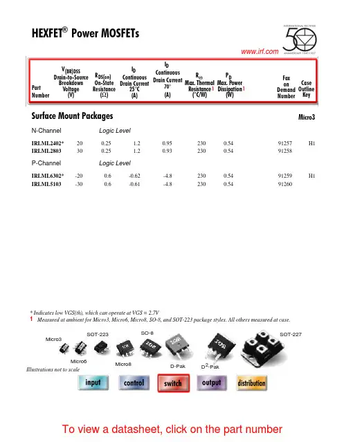
I DContinuous Drain Current(A)70°Micro3Surface Mount PackagesV (BR)DSSDrain-to-Source Breakdown Voltage (V)R DS(on)On-State Resistance ()ΩI D Continuous Drain Current 25°C(A)R ΘMax.Thermal Resistance (°C/W)1FaxonDemand Number Case Outline KeyPartNumberPD Max.PowerDissipation (W)N-ChannelLogic LevelIRLML2402*912570.54200.25 1.20.95230H1IRLML2803912580.54300.251.20.93230P-ChannelLogic LevelIRLML6302*912590.54-200.6-0.62-4.8230H1IRLML5103912600.54-300.6-0.61-4.8230* Indicates low VGS(th), which can operate at VGS = 2.7VMeasured at ambient for Micro3, Micro6, Micro8, SO-8, and SOT-223 package styles. All others measured at case.1Micro3SO-8D-PakD -PakSOT-227Micro6SOT-223Micro82 Illustrations not to scaleI DContinuous Drain Current(A)70°Micro6Surface Mount PackagesV (BR)DSSDrain-to-Source Breakdown Voltage (V)R DS(on)On-State Resistance ()ΩI D Continuous Drain Current 25°C(A)R ΘMax.Thermal Resistance (°C/W)1FaxonDemand Number Case Outline KeyPartNumberPD Max.PowerDissipation (W)N-ChannelLogic LevelIRLMS1902915401.7200.10 3.2 2.675H2IRLMS1503915081.7300.103.22.675P-ChannelLogic LevelIRLMS6702*914141.7-200.20-2.3-1.975H2IRLMS5703914131.7-300.20-2.3-1.975* Indicates low VGS(th), which can operate at VGS = 2.7VMeasured at ambient for Micro3, Micro6, Micro8, SO-8, and SOT-223 package styles. All others measured at case.1Micro3SO-8D-PakD -PakSOT-227Micro6SOT-223Micro82 Illustrations not to scaleI DContinuous Drain Current(A)70°Micro8Surface Mount PackagesV (BR)DSSDrain-to-Source Breakdown Voltage (V)R DS(on)On-State Resistance ()ΩI D Continuous Drain Current 25°C(A)R ΘMax.Thermal Resistance (°C/W)1FaxonDemand Number Case Outline KeyPart NumberP D Max.PowerDissipation (W)N-Channel Logic LevelIRF7601* 912611.820 0.035 5.7 4.6 70 H3IRF7603 912621.830 0.035 5.6 4.5 70Dual N-Channel Logic LevelIRF7501* 912651.220 0.135 2.4 1.9 100 H3IRF7503 912661.2530 0.135 2.4 1.9 100P-Channel Logic LevelIRF7604* 912631.8-20 0.09 -3.6 -2.9 70 H3IRF7606 912641.8-30 0.09 -3.6 -2.9 70Dual P-Channel Logic LevelIRF7504* 912671.25-20 0.27 -1.7 -1.4 100 H3IRF7506 912681.25-30 0.27 -1.7 -1.4 100Dual N- and P-Channel Logic LevelIRF7507* 912691.2520 0.1352.4 1.9 100 H3-20 0.27 -1.7 -1.4IRF7509 912701.2530 0.135 2.4 1.9 100-30 0.27 -1.7 -1.4* Indicates low VGS(th), which can operate at VGS = 2.7VMeasured at ambient for Micro3, Micro6, Micro8, SO-8, and SOT-223 package styles. All others measured at case.1Micro3SO-8D-Pak D -PakSOT-227Micro6SOT-223Micro8 2 Illustrations not to scaleI DContinuous Drain Current(A)70°SO-8Surface Mount PackagesV (BR)DSSDrain-to-Source Breakdown Voltage (V)R DS(on)On-State Resistance ()ΩI D Continuous Drain Current 25°C(A)R ΘMax.Thermal Resistance (°C/W)1FaxonDemand Number Case Outline KeyPart Number P D Max.PowerDissipation (W)N-ChannelIRF7413913302.5300.011139.250H4IRF7413A 916132.5300.0135128.450IRF9410915622.5300.0375.850Dual N-ChannelIRF7311914352.0200.029 6.6 5.362.5H4IRF7313914802.0300.029 6.5 5.262.5IRF7333917002.0300.10 3.5 2.862.5917002.0300.050 4.9 3.962.5IRF9956915592.0300.103.52.862.5Dual P-ChannelIRF7314914352.0-200.058-5.3-4.362.5H4IRF7316915052.0-300.058-4.9-3.962.5IRF9953915602.0-300.25-2.3-1.862.5* Indicates low VGS(th), which can operate at VGS = 2.7VMeasured at ambient for Micro3, Micro6, Micro8, SO-8, and SOT-223 package styles. All others measured at case.1Micro3SO-8D-PakD -PakSOT-227Micro6SOT-223Micro82 Illustrations not to scaleI DContinuous Drain Current(A)70°SO-8Surface Mount PackagesV (BR)DSSDrain-to-Source Breakdown Voltage (V)R DS(on)On-State Resistance ()ΩI D Continuous Drain Current 25°C(A)RΘMax.ThermalResistance(°C/W)1FaxonDemand Number Case Outline KeyPart NumberP D Max.PowerDissipation (W)Dual N- and P-ChannelIRF7317 915682.020 0.029 6.6 5.3 62.5 H42.0-20 0.058 -5.3 -4.3 62.5IRF9952 915622.030 0.103.5 2.8 62.5915622.0-30 0.25 -2.3 -1.8 62.5IRF7319 916062.030 0.029 6.5 5.2 62.52.0-30 0.058 -4.9 -3.9 62.5* Indicates low VGS(th), which can operate at VGS = 2.7VMeasured at ambient for Micro3, Micro6, Micro8, SO-8, and SOT-223 package styles. All others measured at case.1Micro3SO-8D-Pak D -PakSOT-227Micro6SOT-223Micro8 2 Illustrations not to scaleI DContinuous Drain Current(A)70°SO-8Surface Mount PackagesV (BR)DSSDrain-to-Source Breakdown Voltage (V)R DS(on)On-State Resistance ()ΩI D Continuous Drain Current 25°C(A)R ΘMax.Thermal Resistance (°C/W)1FaxonDemand Number Case Outline KeyPart Number P D Max.PowerDissipation (W)N-ChannelLogic LevelIRF7401912442.5200.0228.77.050H4IRF7201911002.5300.0307.0 5.650IRF7403912452.5300.0228.55.450Dual N-ChannelLogic LevelIRF7101908712.0200.10 3.5 2.362.5H4IRF7301912382.0200.050 5.2 4.162.5IRF7303912392.0300.050 4.9 3.962.5IRF7103910952.0500.1303.02.362.5P-ChannelLogic LevelIRF7204911032.5-200.060-5.3-4.250H4IRF7404912462.5-200.040-6.7-5.450IRF7205911042.5-300.070-4.6-3.750IRF7406912472.5-300.045-5.8-3.750IRF7416913562.5-300.02-10-7.150* Indicates low VGS(th), which can operate at VGS = 2.7VMeasured at ambient for Micro3, Micro6, Micro8, SO-8, and SOT-223 package styles. All others measured at case.1Micro3SO-8D-PakD -PakSOT-227Micro6SOT-223Micro82 Illustrations not to scaleI DContinuous Drain Current(A)70°SO-8Surface Mount PackagesV (BR)DSSDrain-to-Source Breakdown Voltage (V)R DS(on)On-State Resistance ()ΩI D Continuous Drain Current 25°C(A)R ΘMax.Thermal Resistance (°C/W)1FaxonDemand Number Case Outline KeyPart Number P D Max.PowerDissipation (W)Dual P-ChannelLogic LevelIRF7104910962.0-200.250-2.3-1.862.5H4IRF7304912402.0-200.090-4.3-3.462.5IRF7306912412.0-300.10-3.6-2.962.5Dual N- and P-Channe Logic LevelIRF7307912421.4200.050 4.3 3.490H4-200.090-3.6-2.9IRF7105910972.0250.1093.5 2.862.52-250.25-2.3-1.862IRF7309912432.0300.050 4.9 3.962.5-300.10-3.6-2.9* Indicates low VGS(th), which can operate at VGS = 2.7VMeasured at ambient for Micro3, Micro6, Micro8, SO-8, and SOT-223 package styles. All others measured at case.1Micro3SO-8D-PakD -PakSOT-227Micro6SOT-223Micro82 Illustrations not to scaleI DContinuous Drain Current(A)70°SOT-223Surface Mount PackagesV (BR)DSSDrain-to-Source Breakdown Voltage (V)R DS(on)On-State Resistance ()ΩI D Continuous Drain Current 25°C(A)R ΘMax.Thermal Resistance (°C/W)1FaxonDemand Number Case Outline KeyPart Number P D Max.PowerDissipation (W)N-ChannelIRFL4105913812.1550.045 3.7 3.060H6IRFL110908612.01000.54 1.50.9660IRFL4310913682.11000.20 1.6 1.360IRFL21090868 2.02001.50.960.660IRFL214908622.02502.00.790.560P-ChannelIRFL9110908642.0-1001.2-1.1-0.6960H6N-ChannelLogic LevelIRLL3303913792.1300.031 4.6 3.760H6IRLL014N 914992.1550.14 2.0 1.660IRLL2705913802.1550.043.83.060* Indicates low VGS(th), which can operate at VGS = 2.7VMeasured at ambient for Micro3, Micro6, Micro8, SO-8, and SOT-223 package styles. All others measured at case.1Micro3SO-8D-PakD -PakSOT-227Micro6SOT-223Micro82 Illustrations not to scaleI DContinuous Drain Current(A)100°D-PakSurface Mount PackagesV (BR)DSSDrain-to-Source Breakdown Voltage (V)R DS(on)On-State Resistance ()ΩI D Continuous Drain Current 25°C(A)R ΘMax.Thermal Resistance (°C/W)1FaxonDemand Number Case Outline KeyPart Number P D Max.PowerDissipation (W)N-ChannelIRFR33039164257300.0313321 2.2H7IRFR024N9133638550.0751610 3.3IRFR41059130248550.0452516 2.7IRFR12059131869550.0273723 1.8IRFR11090524251000.54 4.3 2.75IRFR120N 91365391000.219.1 5.8 3.2IRFR391091364521000.11159.5 2.4IRFR2109052625200 1.5 2.6 1.75IRFR22090525422000.8 4.833IRFR21490703252502 2.2 1.45IRFR2249060042250 1.1 3.8 2.43IRFR3109059725400 3.6 1.7 1.15IRFR3209059842400 1.8 3.123IRFR42090599425003 2.4 1.53IRFRC2090637426004.421.33* Indicates low VGS(th), which can operate at VGS = 2.7VMeasured at ambient for Micro3, Micro6, Micro8, SO-8, and SOT-223 package styles. All others measured at case.1Micro3SO-8D-PakD -PakSOT-227Micro6SOT-223Micro82 Illustrations not to scaleI DContinuous Drain Current(A)100°D-PakSurface Mount PackagesV (BR)DSSDrain-to-Source Breakdown Voltage (V)R DS(on)On-State Resistance ()ΩI D Continuous Drain Current 25°C(A)R ΘMax.Thermal Resistance (°C/W)1FaxonDemand Number Case Outline KeyPart Number P D Max.PowerDissipation (W)P-ChannelIRFR55059161057-550.11-18-11 2.2H7IRFR53059140289-550.065-28-18 1.4IRFR90149065425-600.5-5.1-3.25IRFR90249065542-600.28-8.8-5.63IRFR91109051925-100 1.2-3.1-25IRFR91209052042-1000.6-5.6-3.63IRFR9120N 9150739-1000.48-6.5-4.1 3.2IRFR92109052125-2003-1.9-1.25IRFR92209052242-200 1.5-3.6-2.33IRFR92149165850-250 3.0-2.7-1.7 2.5IRFR93109166350-4007.0-1.8-1.12.5* Indicates low VGS(th), which can operate at VGS = 2.7VMeasured at ambient for Micro3, Micro6, Micro8, SO-8, and SOT-223 package styles. All others measured at case.1Micro3SO-8D-PakD -PakSOT-227Micro6SOT-223Micro82 Illustrations not to scaleI DContinuous Drain Current(A)100°D-PakSurface Mount PackagesV (BR)DSSDrain-to-Source Breakdown Voltage (V)R DS(on)On-State Resistance ()ΩI D Continuous Drain Current 25°C(A)R ΘMax.Thermal Resistance (°C/W)1FaxonDemand Number Case Outline KeyPart Number P D Max.PowerDissipation (W)N-ChannelLogic LevelIRLR27039133538300.0452214 3.3H7IRLR33039131657300.0313321 2.2IRLR31039133369300.0194629 1.8IRLR024N 9136338550.0651711 3.3IRLR27059131746550.042415 2.7IRLR29059133469550.0273623 1.8IRLR120N 91541391000.18511 6.9 3.2IRLR341091607521000.10159.52.4* Indicates low VGS(th), which can operate at VGS = 2.7VMeasured at ambient for Micro3, Micro6, Micro8, SO-8, and SOT-223 package styles. All others measured at case.1Micro3SO-8D-PakD -PakSOT-227Micro6SOT-223Micro82 Illustrations not to scaleI DContinuous Drain Current(A)100°D 2PakSurface Mount PackagesV (BR)DSSDrain-to-Source Breakdown Voltage (V)R DS(on)On-State Resistance ()ΩI D Continuous Drain Current 25°C(A)R ΘMax.Thermal Resistance (°C/W)1FaxonDemand Number Case Outline KeyPart NumberP D Max.PowerDissipation (W)N-ChannelIRFZ24NS 913554555 0.07 17 12 3.3 H10IRFZ34NS 913116855 0.04 29 20 2.2IRFZ44NS 9131511055 0.022 49 35 1.4IRFZ46NS 9130512055 0.020 53 37 1.3IRFZ48NS 9140814055 0.016 64 45 1.1IRF1010NS 913723.855 0.011 84 60 40IRF3205S 9130420055 0.008 110 80 0.75IRFZ44ES 9171411060 0.023 48 34 1.4IRF1010ES 9172017060 0.012 83 59 0.90IRF2807S 9151815075 0.013 71 50 1.0IRF520NS 9134047100 0.2 9.5 6.7 3.2IRF530NS 9135263100 0.11 15 11 2.4IRF540NS 91342110100 0.052 27 19 1.6IRF1310NS 91514120100 0.036 36 25 1.3IRF3710S 91310150100 0.028 46 33 1.0IRF3315S 9161794150 0.082 21 15 1.6IRF3415S 91509150150 0.042 37 26 1.0IRFBC20S 9.101450600 4.4 2.2 1.4 2.5IRFBC30S 9101574600 2.2 3.6 2.3 1.7IRFBC40S 91016130600 1.2 6.2 3.9 1.0* Indicates low VGS(th), which can operate at VGS = 2.7VMeasured at ambient for Micro3, Micro6, Micro8, SO-8, and SOT-223 package styles. All others measured at case.1Micro3SO-8D-Pak D -PakSOT-227Micro6SOT-223Micro8 2 Illustrations not to scaleI DContinuous Drain Current(A)100°D 2PakSurface Mount PackagesV (BR)DSSDrain-to-Source Breakdown Voltage (V)R DS(on)On-State Resistance ()ΩI D Continuous Drain Current 25°C(A)R ΘMax.Thermal Resistance (°C/W)1FaxonDemandNumberCase Outline KeyPart NumberP D Max.PowerDissipation (W)IRFBF20S 9166554900 8.0 1.7 1.1 2.3 H10P-ChannelIRF5305S 91386110-55 0.06 -31 -22 1.4 H10IRF4905S 914783.8-55 0.02 -74 -52 40IRF9520NS 9152247-100 0.48 -6.7 -4.8 3.2IRF9530NS 9152375-100 0.20 -14 -9.9 2.0IRF9540NS 9148394-100 0.117 -19 -13 1.6IRF5210S 91405150-100 0.06 -35 -25 1.0* Indicates low VGS(th), which can operate at VGS = 2.7VMeasured at ambient for Micro3, Micro6, Micro8, SO-8, and SOT-223 package styles. All others measured at case.1Micro3SO-8D-Pak D -PakSOT-227Micro6SOT-223Micro8 2 Illustrations not to scaleI DContinuous Drain Current(A)100°D 2PakSurface Mount PackagesV (BR)DSSDrain-to-Source Breakdown Voltage (V)R DS(on)On-State Resistance ()ΩI D Continuous Drain Current 25°C(A)R ΘMax.Thermal Resistance (°C/W)1FaxonDemand Number Case Outline KeyPart NumberP D Max.PowerDissipation (W)N-Channel Logic LevelIRL3302S 916925720 0.020 39 25 2.2 H10IRL3202S916756920 0.016 48 30 1.8IRL3102S 916918920 0.013 61 39 1.4IRL3402S 9169311020 0.01 85 54 1.1IRL3502S 9167614020 0.007 110 67 0.89IRL2703S 913604530 0.04 24 17 3.3IRL3303S 913236830 0.026 38 27 2.2IRL3103S 9133811030 0.014 64 45 1.4IRL2203NS 9136717030 0.007 116 82 0.90IRL3803S 9131920030 0.006 140 98 0.75IRLZ24NS 913584555 0.06 18 13 3.3IRLZ34NS 913086855 0.035 30 21 2.2IRLZ44NS 9134711055 0.022 47 33 1.4IRL3705NS 9150217055 0.01 89 63 0.90IRL2505S 9132620055 0.008 104 74 0.75IRLZ44S 9090615060 0.028 50 36 1.0IRL530NS 9134963100 0.1 15 11 2.4IRL2910S 91376150100 0.026 48 34 1.0* Indicates low VGS(th), which can operate at VGS = 2.7VMeasured at ambient for Micro3, Micro6, Micro8, SO-8, and SOT-223 package styles. All others measured at case.1Micro3SO-8D-Pak D -PakSOT-227Micro6SOT-223Micro8 2 Illustrations not to scaleI DContinuous Drain Current(A)100°SOT-227Surface Mount PackagesV (BR)DSSDrain-to-Source Breakdown Voltage (V)R DS(on)On-State Resistance ()ΩI D Continuous DrainCurrent 25°C(A)RΘMax.Thermal Resistance (°C/W)1FaxonDemand Number Case Outline KeyPart Number P D Max.PowerDissipation (W)N-ChannelFully Isolated Low ChargeFA38SA50LC 916155005000.1338240.25H21FA57SA50LC916506255000.0857360.20* Indicates low VGS(th), which can operate at VGS = 2.7VMeasured at ambient for Micro3, Micro6, Micro8, SO-8, and SOT-223 package styles. All others measured at case.1Micro3SO-8D-PakD -PakSOT-227Micro6SOT-223Micro82 Illustrations not to scaleI DContinuous Drain Current(A)100°I-PakThrough-Hole PackagesV (BR)DSSDrain-to-Source Breakdown Voltage (V)R DS(on)On-State Resistance ()ΩI D Continuous Drain Current 25°C(A)R ΘMax.Thermal Resistance (°C/W)1FaxonDemand Number Case Outline KeyPart Number P D Max.PowerDissipation (W)N-ChannelIRFU33039164257300.0313321 2.2H8IRFU024N 9133638550.0751610 3.3IRFU41059130248550.0452519 2.7IRFU12059131869550.0273723 1.8IRFU11090524251000.54 4.3 2.7 5.0IRFU120N 91365391000.219.1 5.8 3.2IRFU391091364521000.11159.5 2.4IRFU2109052625200 1.5 2.6 1.7 5.0IRFU22090525422000.80 4.8 3.0 3.0IRFU2149070325250 2.0 2.2 1.4 5.0IRFU2249060042250 1.1 3.8 2.4 3.0IRFU3109059725400 3.6 1.7 1.1 5.0IRFU3209059842400 1.8 3.1 2.0 3.0IRFU4209059942500 3.0 2.4 1.5 3.0IRFUC2090637426004.42.01.33.0I-PakTO-220 FullPakTO-262TO-247HEXDIPTO-220AB Illustrations not to scale** Not ratedI DContinuous Drain Current(A)100°I-PakThrough-Hole PackagesV (BR)DSSDrain-to-Source Breakdown Voltage (V)R DS(on)On-State Resistance ()ΩI D Continuous Drain Current 25°C(A)R ΘMax.Thermal Resistance (°C/W)1FaxonDemand Number Case Outline KeyPart Number P D Max.PowerDissipation (W)P-ChannelIRFU55059161057-550.11-18-11 2.2H8IRFU53059140289-550.065-28-18 1.4IRFU90149065425-600.50-5.1-3.2 5.0IRFU90249065542-600.28-8.8-5.6 3.0IRFU91109051925-100 1.2-3.1-2.0 5.0IRFU91209052042-1000.60-5.6-3.6 3.0IRFU9120N 9150739-1000.48-6.5-4.1 3.2IRFU92109052125-200 3.0-1.9-1.2 5.0IRFU92209052242-200 1.5-3.6-2.3 3.0IRFU92149165850-2503.0-2.7-1.7 2.5IRFU93109166350-4007.0-1.8-1.12.5N-ChannelLogic LevelIRLU27039133538300.0452214 3.3H8IRLU33039131657300.0313321 2.2IRLU31039133369300.0194629 1.8IRLU024N 9136338550.0651711 3.3IRLU27059131746550.04241715IRLU29059133469550.0273623 1.8IRLU120N 91541391000.18511 6.9 3.2IRLU341091607521000.10159.52.4I-PakTO-220 FullPakTO-262TO-247HEXDIPTO-220AB Illustrations not to scale** Not ratedI DContinuous Drain Current(A)100°HEXDIPThrough-Hole PackagesV (BR)DSSDrain-to-Source Breakdown Voltage (V)R DS(on)On-State Resistance ()ΩI D Continuous Drain Current 25°C(A)R ΘMax.Thermal Resistance (°C/W)1FaxonDemand Number Case Outline KeyPart Number P D Max.PowerDissipation (W)N-ChannelIRFD014907001.3600.2 1.7 1.2120H9IRFD024906991.3600.1 2.5 1.8120IRFD110903281.31000.54 1.00.71120IRFD120903851.31000.27 1.30.94120IRFD210903861.3200 1.50.60.38120IRFD220904171.32000.80.80.50120IRFD214912711.3250 2.00.570.32120IRFD224912721.3250 1.10.760.43120IRFD310912251.3400 3.60.420.23120IRFD320912261.3400 1.80.600.33120IRFD420912271.3500 3.00.460.26120IRFDC20912281.36004.40.320.21120I-PakTO-220 FullPakTO-262TO-247HEXDIPTO-220AB Illustrations not to scale** Not ratedI D Continuous Drain Current (A)100°TO-220Qg TotalGate Charge(nC)Through-Hole PackagesV (BR)DSSDrain-to-Source Breakdown Voltage (V)R DS(on)On-State Resistance ()ΩI D Continuous Drain Current 25°C (A)R ΘMax.Thermal Resistance(°C/W)1Faxon Demand Number Case OutlineKeyPart Number P D Max.Power Dissipation (W)N-ChannelLow ChargeIRF737LC91314743000.75 6.1** 1.7 3.9H11IRF740LC 910681254000.5510** 1.039IRF840LC 910691255000.858.0** 1.039IRFBC40LC910701256001.26.2**1.039I-PakTO-220 FullPakTO-262TO-247HEXDIPTO-220AB Illustrations not to scale** Not ratedI DContinuous Drain Current(A)100°TO-220ABThrough-Hole PackagesV (BR)DSSDrain-to-Source Breakdown Voltage (V)R DS(on)On-State Resistance ()ΩI D Continuous Drain Current 25°C(A)R ΘMax.Thermal Resistance (°C/W)1FaxonDemand Number Case Outline KeyPart Number P D Max.PowerDissipation (W)N-ChannelIRFZ24N 9135445550.071712 3.3H12IRFZ34N9127656550.042618 2.7IRFZ44N 9130383550.0244129 1.8IRFZ46N 9127788550.024633 1.7IRFZ48N 9140694550.0165337 1.6IRF1010N 91278130550.0127251 1.2IRF320591279150550.0089869 1.0IRFZ34E 9167268600.0422820 2.2IRFZ44E 91671110600.0234834 1.4IRF1010E 91670170600.01281570.90IRF280791517150750.0137150 1.0IRF520N 91339471000.209.5 6.79.5IRF530N 91351601000.111511 2.4IRF540N 91341941000.0522719 1.6IRF1310N 916111201000.0363625 1.3IRF3710913091501000.0284633 1.0IRF331591623941500.0822115 1.6IRF3415914771501500.0423726 1.0IRFBC209062350600 4.4 2.2 1.4 2.5IRFBC309048274600 2.2 3.6 2.3 1.7IRFBC4090506125600 1.2 6.2 3.9 1.0IRFBE2090610548006.51.81.22.3I-PakTO-220 FullPakTO-262TO-247HEXDIPTO-220AB Illustrations not to scale** Not ratedI DContinuous Drain Current(A)100°TO-220ABThrough-Hole PackagesV (BR)DSSDrain-to-Source Breakdown Voltage (V)R DS(on)On-State Resistance ()ΩI D Continuous Drain Current 25°C(A)R ΘMax.Thermal Resistance (°C/W)1FaxonDemand Number Case Outline KeyPart Number P D Max.PowerDissipation (W)IRFBE3090613125800 3.0 4.1 2.6 2.0H12IRFBF3090616125900 3.7 3.6 2.3 1.0IRFBG209060454100011 1.40.86 2.3IRFBG309062012510005.03.12.01.0P-ChannelIRF9Z24N 9148445-550.175-12-8.53.3H12IRF9Z34N 9148556-550.10-17-12 2.7IRF530591385110-550.06-31-22 1.4IRF490591280150-550.02-64-45 1.0IRF9530N 9148275-1000.20-13-9.2 2.0IRF9540N 9143794-1000.117-19-13 1.6IRF521091434150-1000.06-35-25 1.0IRF62159147983-1500.29-11-7.81.8I-PakTO-220 FullPakTO-262TO-247HEXDIPTO-220AB Illustrations not to scale** Not ratedI DContinuous Drain Current(A)100°TO-220ABThrough-Hole PackagesV (BR)DSSDrain-to-Source Breakdown Voltage (V)R DS(on)On-State Resistance ()ΩI D Continuous Drain Current 25°C(A)R ΘMax.Thermal Resistance (°C/W)1FaxonDemand Number Case Outline KeyPart NumberP D Max.PowerDissipation (W)N-Channel Logic LevelIRL3302 916965720 0.020 39 25 2.2 H12IRL3202 916956920 0.016 48 30 1.8IRL3102 916948920 0.013 61 39 1.4IRL3402 9169711020 0.01 85 54 1.1IRL3502 9169814020 0.007 110 67 0.89IRL2703 913594530 0.04 24 17 3.3IRL3303 913225630 0.026 34 24 2.7IRL3103 913378330 0.014 56 40 1.8IRL2203N 9136613030 0.007 100 71 1.230 0.007 61 43 3.2IRL3803 9130115030 0.006 120 83 1.0IRLZ24N 913574555 0.06 18 13 3.3IRLZ34N 913075655 0.035 27 19 2.7IRLZ44N 913468355 0.022 41 29 1.8IRL3705N 9137013055 0.01 77 54 1.2IRL2505 9132520055 0.008 104 74 0.75IRL520N 9149447100 0.18 10 7.1 3.2IRL530N 9134863100 0.10 15 11 2.4IRL540N 9149594100 0.044 30 21 1.6IRL2910 91375150100 0.026 48 34 1.0I-PakTO-220 FullPakTO-262TO-247HEXDIPTO-220AB Illustrations not to scale** Not ratedI D Continuous Drain Current (A)100°TO-220 FullPak (Fully Isolated)Qg TotalGate Charge(nC)Through-Hole PackagesV (BR)DSSDrain-to-Source Breakdown Voltage (V)R DS(on)On-State Resistance ()ΩI D Continuous DrainCurrent 25°C(A)R ΘMax.Thermal Resistance (°C/W)1Fax on Demand Number Case OutlineKeyPart Number P D Max.Power Dissipation (W)N-ChannelLow ChargeIRFI740GLC91209404000.55 6.0** 3.139H13IRFI840GLC 91208405000.85 4.8** 3.139IRFIBC40GLC91211406001.24.0**3.139I-PakTO-220 FullPakTO-262TO-247HEXDIPTO-220AB Illustrations not to scale** Not ratedI DContinuous Drain Current(A)100°TO-220 FullPak (Fully Isolated)Through-Hole PackagesV (BR)DSSDrain-to-Source Breakdown Voltage (V)R DS(on)On-State Resistance ()ΩI D Continuous Drain Current 25°C(A)R ΘMax.Thermal Resistance (°C/W)1FaxonDemand Number Case Outline KeyPart Number P D Max.PowerDissipation (W)N-ChannelIRFIZ24N 9150126550.07139.2 5.8H14IRFIZ34N9148931550.041913 4.8IRFIZ44N 9140338550.02428200.024IRFIZ46N 9130640550.023122 3.8IRFIZ48N 9140742550.0163625 3.6IRFI1010N 9137347550.0124431 3.2IRFI32059137448550.0085640 3.1IRFIZ24E 9167329600.071149.6 5.2IRFIZ34E 9167437600.0422115 4.1IRFI510G 90829271000.54 4.5 3.2 5.5IRFI520N 91362271000.207.2 5.1 5.5IRFI530N 91353331000.11117.8 4.5IRFI540N 91361421000.0521813 3.6IRFI1310N 91611451000.0362216 3.3IRFI371091387481000.0252820 3.1IRFI620G 90832302000.8 4.1 2.6 4.1IRFI630G 90652322000.4 5.9 3.7 3.6IRFI640G 90649402000.189.8 6.2 3.1IRFI614G 9083123250 2.0 2.1 1.3 5.5IRFI624G 9083330250 1.1 3.4 2.2 4.1IRFI634G 90738322500.45 5.6 3.5 3.6IRFI644G 90739402500.287.953.1I-PakTO-220 FullPakTO-262TO-247HEXDIPTO-220AB Illustrations not to scale** Not ratedI DContinuous Drain Current(A)100°TO-220 FullPak (Fully Isolated)Through-Hole PackagesV (BR)DSSDrain-to-Source Breakdown Voltage (V)R DS(on)On-State Resistance ()ΩI D Continuous Drain Current 25°C(A)R ΘMax.Thermal Resistance (°C/W)1FaxonDemand Number Case Outline KeyPart Number P D Max.PowerDissipation (W)IRFI720G 9083430400 1.8 2.6 1.7 4.1H14IRFI730G 9065032400 1.0 3.7 2.3 3.6IRFI740G 90651404000.55 5.4 3.4 3.1IRFI734G 9100135450 1.2 3.4 2.1 3.6IRFI744G 91002404500.63 4.9 3.1 3.1IRFI820G 9064130500 3.0 2.1 1.3 4.1IRFI830G 9064632500 1.5 3.12 3.6IRFI840G 90642405000.85 4.6 2.9 3.1IRFIBC20G 90850306004.41.71.1 4.1IRFIBC30G 90851356002.2 2.5 1.63.6IRFIBC40G 9085240600 1.2 3.5 2.2 3.1IRFIBE20G 9085330800 6.5 1.4.86 4.1IRFIBE30G 9085435800 3.0 2.1 1.4 3.6IRFIBF20G 90855309008.0 1.2.79 4.1IRFIBF30G90856359003.71.91.23.6P-ChannelIRFI9Z24N 9152929-550.175-9.5-6.7 5.2H14IRFI9Z34N 9153037-550.10-14-10 4.1IRFI49059152663-550.02-41-29 2.4IRFI9540G 9083742-1000.117-13-9.2 3.6IRFI9540N 9148742-1000.117-13-9.2 3.6IRFI52109140448-1000.06-20-14 3.1IRFI9634G 9148835-2501.0-4.1-2.63.6I-PakTO-220 FullPakTO-262TO-247HEXDIPTO-220AB Illustrations not to scale** Not ratedI DContinuous Drain Current(A)100°TO-220 FullPak (Fully Isolated)Through-Hole PackagesV (BR)DSSDrain-to-Source Breakdown Voltage (V)R DS(on)On-State Resistance ()ΩI D Continuous Drain Current 25°C(A)R ΘMax.Thermal Resistance (°C/W)1FaxonDemand Number Case Outline KeyPart Number P D Max.PowerDissipation (W)N-ChannelLogic LevelIRLI2203N 9137847300.0076143 3.2H14IRLI38039132048300.0066747 3.1IRLIZ24N 9134426550.06149.9 5.8IRLIZ34N 9132931550.0352014 4.8IRLIZ44N 9149838550.0222820 4.0IRLI3705N 9136947550.014733 3.2IRLI25059132763550.00858412.4IRLI520N 91496271000.187.7 5.4 5.5IRLI530N 91350331000.10117.8 4.5IRLI540N 91497421000.04420143.6IRLI291091384481000.02627193.1P-ChannelLogic LevelIRFI9520G 9083537-1000.6-5.2-3.6 4.1H14IRFI9530G 9083638-1000.03-7.7-5.4 3.6IRFI9620G 9087430-200 1.5-3.0-1.9 4.1IRFI9630G 9083840-2000.8-4.3-2.7 3.6IRFI9640G9083940-2000.5-6.1-3.93.1I-PakTO-220 FullPakTO-262TO-247HEXDIPTO-220AB Illustrations not to scale** Not ratedI D Continuous Drain Current (A)100°TO-247Qg TotalGate Charge(nC)Through-Hole PackagesV (BR)DSSDrain-to-Source Breakdown Voltage (V)R DS(on)On-State Resistance ()ΩI D Continuous Drain Current 25°C (A)R ΘMax.Thermal Resistance (°C/W)1Fax on Demand Number Case OutlineKeyPart Number P D Max.Power Dissipation (W)1N-ChannelLow ChargeIRFP350LC912291904000.3018**0.6570H16IRFP360LC 912302804000.2023**0.4598IRFP450LC 912311905000.4016**0.6570IRFP460LC 912322805000.2720**0.4598IRFPC50LC 912331906000.6013**0.6570IRFPC60LC912342806000.4016**0.4598I-PakTO-220 FullPakTO-262TO-247HEXDIPTO-220AB Illustrations not to scale** Not rated。
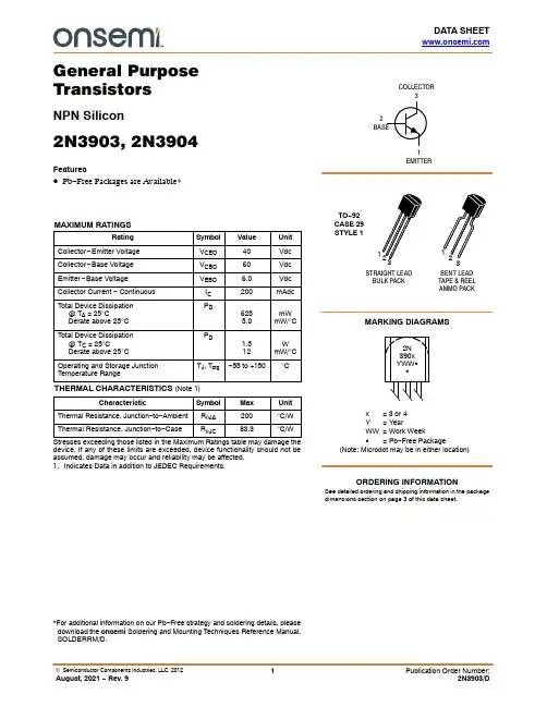
DATA SHEET General PurposeTransistorsNPN Silicon2N3903, 2N3904Features•Pb−Free Packages are Available*MAXIMUM RATINGSRating Symbol Value UnitCollector−Emitter Voltage V CEO40VdcCollector−Base Voltage V CBO60VdcEmitter−Base Voltage V EBO 6.0VdcCollector Current − Continuous I C200mAdcTotal Device Dissipation @ T A = 25°CDerate above 25°C P D6255.0mWmW/°CTotal Device Dissipation@ T C = 25°C Derate above 25°C P D1.512WmW/°COperating and Storage Junction Temperature Range T J, T stg−55 to +150°CTHERMAL CHARACTERISTICS (Note 1)Characteristic Symbol Max Unit Thermal Resistance, Junction−to−Ambient R q JA200°C/W Thermal Resistance, Junction−to−Case R q JC83.3°C/W Stresses exceeding those listed in the Maximum Ratings table may damage the device. If any of these limits are exceeded, device functionality should not be assumed, damage may occur and reliability may be affected.1.Indicates Data in addition to JEDEC Requirements.*For additional information on our Pb−Free strategy and soldering details, please download the onsemi Soldering and Mounting T echniques Reference Manual, SOLDERRM/D.MARKING DIAGRAMSSee detailed ordering and shipping information in the package dimensions section on page 3 of this data sheet.ORDERING INFORMATIONCOLLECTOR21EMITTER2N390xYWW GGx= 3 or 4Y= YearWW= Work WeekG= Pb−Free Package(Note: Microdot may be in either location)BENT LEADTAPE & REELAMMO PACKSTRAIGHT LEADBULK PACKTO−92CASE 29STYLE 1ELECTRICAL CHARACTERISTICS (T A = 25°C unless otherwise noted)Characteristic Symbol Min Max Unit OFF CHARACTERISTICSCollector−Emitter Breakdown Voltage (Note 2)(I C = 1.0 mAdc, I B = 0)V(BR)CEO40−Vdc Collector−Base Breakdown Voltage (I C = 10 m Adc, I E = 0)V(BR)CBO60−Vdc Emitter−Base Breakdown Voltage (I E = 10 m Adc, I C = 0)V(BR)EBO 6.0−Vdc Base Cutoff Current (V CE = 30 Vdc, V EB = 3.0 Vdc)I BL−50nAdc Collector Cutoff Current (V CE = 30 Vdc, V EB = 3.0 Vdc)I CEX−50nAdc ON CHARACTERISTICSDC Current Gain (Note 2)(I C = 0.1 mAdc, V CE = 1.0 Vdc)2N39032N3904 (I C = 1.0 mAdc, V CE = 1.0 Vdc)2N39032N3904 (I C = 10 mAdc, V CE = 1.0 Vdc)2N39032N3904 (I C = 50 mAdc, V CE = 1.0 Vdc)2N39032N3904 (I C = 100 mAdc, V CE = 1.0 Vdc)2N39032N3904h FE204035705010030601530−−−−150300−−−−−Collector−Emitter Saturation Voltage (Note 2) (I C = 10 mAdc, I B = 1.0 mAdc)(I C = 50 mAdc, I B = 5.0 mAdc V CE(sat)−−0.20.3VdcBase−Emitter Saturation Voltage (Note 2) (I C = 10 mAdc, I B = 1.0 mAdc)(I C = 50 mAdc, I B = 5.0 mAdc)V BE(sat)0.65−0.850.95VdcSMALL−SIGNAL CHARACTERISTICSCurrent−Gain − Bandwidth Product(I C = 10 mAdc, V CE = 20 Vdc, f = 100 MHz)2N39032N3904f T250300−−MHzOutput Capacitance (V CB = 5.0 Vdc, I E = 0, f = 1.0 MHz)C obo− 4.0pF Input Capacitance (V EB = 0.5 Vdc, I C = 0, f = 1.0 MHz)C ibo−8.0pFInput Impedance(I C = 1.0 mAdc, V CE = 10 Vdc, f = 1.0 kHz)2N39032N3904h ie1.01.08.010k WVoltage Feedback Ratio(I C = 1.0 mAdc, V CE = 10 Vdc, f = 1.0 kHz)2N39032N3904h re0.10.55.08.0X 10−4Small−Signal Current Gain(I C = 1.0 mAdc, V CE = 10 Vdc, f = 1.0 kHz)2N39032N3904h fe50100200400−Output Admittance (I C = 1.0 mAdc, V CE = 10 Vdc, f = 1.0 kHz)h oe 1.040m mhosNoise Figure(I C = 100 m Adc, V CE = 5.0 Vdc, R S = 1.0 k W, f = 1.0 kHz)2N39032N3904NF−−6.05.0dBSWITCHING CHARACTERISTICSDelay Time(VCC = 3.0 Vdc, V BE = 0.5 Vdc,I C = 10 mAdc, I B1 = 1.0 mAdc)t d−35nsRise Time t r−35nsStorage Time(V CC = 3.0 Vdc, I C = 10 mAdc,2N3903I B1 = I B2 = 1.0 mAdc)2N3904t s−−175200nsFall Time t f−50ns 2.Pulse Test: Pulse Width v 300 m s; Duty Cycle v 2%.ORDERING INFORMATIONDevicePackage Shipping †2N3903RLRM TO −922000 / Ammo Pack 2N3904TO −925000 Units / Bulk 2N3904G TO −92(Pb −Free)5000 Units / Bulk 2N3904RLRA TO −922000 / Tape & Reel 2N3904RLRAG TO −92(Pb −Free)2000 / Tape & Reel 2N3904RLRM TO −922000 / Ammo Pack 2N3904RLRMG TO −92(Pb −Free)2000 / Ammo Pack 2N3904RLRPTO −922000 / Ammo Pack 2N3904RLRPG TO −92(Pb −Free)2000 / Ammo Pack 2N3904RL1G TO −92(Pb−Free)2000 / Tape & Reel 2N3904ZL1TO −922000 / Ammo Pack 2N3904ZL1GTO −92(Pb −Free)2000 / Ammo Pack†For information on tape and reel specifications, including part orientation and tape sizes, please refer to our Tape and Reel Packaging Specifications Brochure, BRD8011/D.Figure 1. Delay and Rise Time Equivalent Test CircuitFigure 2. Storage and Fall Time Equivalent Test Circuit10 < t 1 < 500 m * T otal shunt capacitance of test jig and connectors* T otal shunt capacitance of test jig and connectorsTYPICAL TRANSIENT CHARACTERISTICSFigure 3. CapacitanceREVERSE BIAS VOLTAGE (VOLTS)2.03.05.07.0101.00.1Figure 4. Charge DataI C , COLLECTOR CURRENT (mA)50001.0Q , C H A R G E (p C )3000200010005003002007001005070 2.0 3.0 5.07.01020305070100200C A P A C I T A N C E (p F )1.02.03.0 5.07.010200.20.30.50.7T J = 25°C T J = 125°CFigure 5. Turn −On TimeI C , COLLECTOR CURRENT (mA)7010020030050050Figure 6. Rise TimeI C , COLLECTOR CURRENT (mA)T I M E (n s )5t , R I S E T I M E (n s )Figure 7. Storage Time I C , COLLECTOR CURRENT (mA)Figure 8. Fall TimeI C , COLLECTOR CURRENT (mA)1030720701002003005005051030720701002003005005051030720701002003005005051030720r t , F A L L T I M E (n s )f t , S T O R A G E T I M E (n s )s ′TYPICAL AUDIO SMALL −SIGNAL CHARACTERISTICSNOISE FIGURE VARIATIONS(V CE = 5.0 Vdc, T A = 25°C, Bandwidth = 1.0 Hz)Figure 9. f, FREQUENCY (kHz)46810122Figure 10.R S , SOURCE RESISTANCE (k OHMS)0N F , N O I S E F I G U R E (d B )04681012214N F , N O I S E F I G U R E (d B )Figure 11. Current GainI C , COLLECTOR CURRENT (mA)7010020030050Figure 12. Output AdmittanceI C , COLLECTOR CURRENT (mA)h , C U R R E N T G A I Nh , O U T P U T A D M I T T A N C E ( m h o s )Figure 13. Input Impedance I C , COLLECTOR CURRENT (mA)Figure 14. Voltage Feedback RatioI C , COLLECTOR CURRENT (mA)3010050510202.03.05.07.0101.00.10.21.02.0 5.00.5100.30.5 3.00.72.05.010201.00.20.5o e h , V O L T A G E F E E D B A C K R A T I O (X 10 )r e h , I N P U T I M P E D A N C E (k O H M S )ie 0.10.21.02.0 5.0100.30.5 3.00.10.21.02.0 5.0100.30.5 3.0210.10.21.02.0 5.0100.30.5 3.0f e m -4h PARAMETERS(V CE = 10 Vdc, f = 1.0 kHz, T A = 25°C)TYPICAL STATIC CHARACTERISTICSFigure 15. DC Current GainI C , COLLECTOR CURRENT (mA)0.30.50.71.02.00.2h , D C C U R R E N T G A I N (N O R M A L I Z E D )0.1F EFigure 16. Collector Saturation RegionI B , BASE CURRENT (mA)0.40.60.81.00.2V , C O L L E C T O R E M I T T E R V O L T A G E (V O L T S )0CE Figure 17. “ON” Voltages I C , COLLECTOR CURRENT (mA)0.40.60.81.01.20.2Figure 18. Temperature CoefficientsI C , COLLECTOR CURRENT (mA)V , V O L T A G E (V O L T S )- 0.500.51.0C O E F F I C I E N T (m V / C )- 1.0- 1.5- 2.0°TO−92 (TO−226)CASE 29−11ISSUE AMDATE 09 MAR 2007STYLES ON PAGE 2NOTES:1.DIMENSIONING AND TOLERANCING PER ANSIY14.5M, 1982.2.CONTROLLING DIMENSION: INCH.3.CONTOUR OF PACKAGE BEYOND DIMENSION RIS UNCONTROLLED.4.LEAD DIMENSION IS UNCONTROLLED IN P ANDBEYOND DIMENSION K MINIMUM.SECTION X−XPLANE DIM MIN MAX MIN MAXMILLIMETERSINCHESA0.1750.205 4.45 5.20B0.1700.210 4.32 5.33C0.1250.165 3.18 4.19D0.0160.0210.4070.533G0.0450.055 1.15 1.39H0.0950.105 2.42 2.66J0.0150.0200.390.50K0.500---12.70---L0.250--- 6.35---N0.0800.105 2.04 2.66P---0.100--- 2.54R0.115--- 2.93---V0.135--- 3.43---BENT LEADTAPE & REELAMMO PACKSTRAIGHT LEADBULK PACKNOTES:1.DIMENSIONING AND TOLERANCING PERASME Y14.5M, 1994.2.CONTROLLING DIMENSION: MILLIMETERS.3.CONTOUR OF PACKAGE BEYONDDIMENSION R IS UNCONTROLLED.4.LEAD DIMENSION IS UNCONTROLLED IN PAND BEYOND DIMENSION K MINIMUM.SECTION X−XDIM MIN MAXMILLIMETERSA 4.45 5.20B 4.32 5.33C 3.18 4.19D0.400.54G 2.40 2.80J0.390.50K12.70---N 2.04 2.66P 1.50 4.00R 2.93---V 3.43---STRAIGHT LEADBULK PACKBENT LEADTAPE & REELAMMO PACKMECHANICAL CASE OUTLINEPACKAGE DIMENSIONSTO−92 (TO−226)CASE 29−11ISSUE AMDATE 09 MAR 2007STYLE 1:PIN 1.EMITTER2.BASE3.COLLECTORSTYLE 6:PIN 1.GATE2.SOURCE & SUBSTRATE3.DRAINSTYLE 11:PIN 1.ANODE2.CATHODE & ANODE3.CATHODESTYLE 16:PIN 1.ANODE2.GATE3.CATHODESTYLE 21:PIN 1.COLLECTOR2.EMITTER3.BASESTYLE 26:PIN 1.V CC2.GROUND 23.OUTPUTSTYLE 31:PIN 1.GATE2.DRAIN3.SOURCE STYLE 2:PIN 1.BASE2.EMITTER3.COLLECTORSTYLE 7:PIN 1.SOURCE2.DRAIN3.GATESTYLE 12:PIN 1.MAIN TERMINAL 12.GATE3.MAIN TERMINAL 2STYLE 17:PIN 1.COLLECTOR2.BASE3.EMITTERSTYLE 22:PIN 1.SOURCE2.GATE3.DRAINSTYLE 27:PIN 1.MT2.SUBSTRATE3.MTSTYLE 32:PIN 1.BASE2.COLLECTOR3.EMITTERSTYLE 3:PIN 1.ANODE2.ANODE3.CATHODESTYLE 8:PIN 1.DRAIN2.GATE3.SOURCE & SUBSTRATESTYLE 13:PIN 1.ANODE 12.GATE3.CATHODE 2STYLE 18:PIN 1.ANODE2.CATHODE3.NOT CONNECTEDSTYLE 23:PIN 1.GATE2.SOURCE3.DRAINSTYLE 28:PIN 1.CATHODE2.ANODE3.GATESTYLE 33:PIN 1.RETURN2.INPUT3.OUTPUTSTYLE 4:PIN 1.CATHODE2.CATHODE3.ANODESTYLE 9:PIN 1.BASE 12.EMITTER3.BASE 2STYLE 14:PIN 1.EMITTER2.COLLECTOR3.BASESTYLE 19:PIN 1.GATE2.ANODE3.CATHODESTYLE 24:PIN 1.EMITTER2.COLLECTOR/ANODE3.CATHODESTYLE 29:PIN 1.NOT CONNECTED2.ANODE3.CATHODESTYLE 34:PIN 1.INPUT2.GROUND3.LOGICSTYLE 5:PIN 1.DRAIN2.SOURCE3.GATESTYLE 10:PIN 1.CATHODE2.GATE3.ANODESTYLE 15:PIN 1.ANODE 12.CATHODE3.ANODE 2STYLE 20:PIN 1.NOT CONNECTED2.CATHODE3.ANODESTYLE 25:PIN 1.MT 12.GATE3.MT 2STYLE 30:PIN 1.DRAIN2.GATE3.SOURCESTYLE 35:PIN 1.GATE2.COLLECTOR3.EMITTERON Semiconductor and are registered trademarks of Semiconductor Components Industries, LLC (SCILLC). SCILLC reserves the right to make changes without further notice to any products herein. SCILLC makes no warranty, representation or guarantee regarding the suitability of its products for any particular purpose, nor does SCILLC assume any liability arising out of the application or use of any product or circuit, and specifically disclaims any and all liability, including without limitation special, consequential or incidental damages.“Typical” parameters which may be provided in SCILLC data sheets and/or specifications can and do vary in different applications and actual performance may vary over time. All operating parameters, including “Typicals” must be validated for each customer application by customer’s technical experts. SCILLC does not convey any license under its patent rights nor the rights of others. SCILLC products are not designed, intended, or authorized for use as components in systems intended for surgical implant into the body, or other applications intended to support or sustain life, or for any other application in which the failure of the SCILLC product could create a situation where personal injury or death may occur. Should Buyer purchase or use SCILLC products for any such unintended or unauthorized application, Buyer shall indemnify and hold SCILLC and its officers, employees, subsidiaries, affiliates, and distributors harmless against all claims, costs, damages, and expenses, and reasonable attorney fees arising out of, directly or indirectly, any claim of personal injury or deathassociated with such unintended or unauthorized use, even if such claim alleges that SCILLC was negligent regarding the design or manufacture of the part. SCILLC is an EqualPUBLICATION ORDERING INFORMATIONTECHNICAL SUPPORTNorth American Technical Support:LITERATURE FULFILLMENT :Email Requests to:*******************Europe, Middle East and Africa Technical Support:。
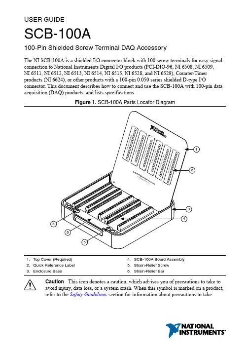
USER GUIDESCB-100A100-Pin Shielded Screw Terminal DAQ AccessoryThe NI SCB-100A is a shielded I/O connector block with 100 screw terminals for easy signal connection to National Instruments Digital I/O products (PCI-DIO-96, NI 6508, NI 6509,NI 6511, NI 6512, NI 6513, NI 6514, NI 6515, NI 6528, and NI 6529), Counter/Timer products (NI 6624), or other products with a 100-pin 0.050 series shielded D-type I/Oconnector. This document describes how to connect and use the SCB-100A with 100-pin data acquisition (DAQ) products, and lists specifications.Figure 1. SCB-100A Parts Locator Diagram1.Top Cover (Required)2.Quick Reference Label3.Enclosure Base4.SCB-100A Board Assembly5.Strain-Relief Screw6.Strain-Relief BarCaution This icon denotes a caution, which advises you of precautions to take toavoid injury, data loss, or a system crash. When this symbol is marked on a product,refer to the Safety Guidelines section for information about precautions to take.Safety GuidelinesThe following cautions contain important safety information concerning hazardous voltages and connector blocks.Caution Do not connect hazardous voltages (>30 V RMS/42 V peak/60 V DC).Refer to your product documentation for information about the electrical limits ofyour device or module.Caution Install cover prior to use. To avoid electrical shock, do not removeSCB-100A covers unless you are qualified to do so. Before removing the cover,disconnect any live circuit from the connector block. Replace cover for use.Caution The chassis ground lug on your SCB-100A is for groundinghigh-impedance sources, such as a floating source (1 mA maximum) and forterminating the shields of connected cables. Do not use the chassis ground lug as asafety earth ground.Electromagnetic Compatibility GuidelinesThis product was tested and complies with the regulatory requirements and limits for electromagnetic compatibility (EMC) as stated in the product specifications. These requirements and limits are designed to provide reasonable protection against harmful interference when the product is operated in its intended operational electromagnetic environment.This product is intended for use in residential, commercial, and industrial locations. However, harmful interference may occur in some installations or when the product is connected to a peripheral device or a test object. To minimize interference with radio and television reception and prevent unacceptable performance degradation, install and use this product in strict accordance with the instructions in the product documentation.Furthermore, any changes or modifications to the product not expressly approved by National Instruments could void your authority to operate it under your local regulatory rules.Caution To ensure the specified EMC performance, operate this product only withshielded cables and accessories.Caution To ensure the specified EMC performance, signal wires routed outside ofthe enclosure must be contained within a shielded cable and connected to shieldedaccessories. Cable shields must be terminated to the chassis ground lug using asshort a connection as is practical.2| | SCB-100A User GuideWhat Y ou Need to Get StartedTo set up and use your SCB-100A, you need the items shown in the following figure. You can find quick reference labels, which specify accessory pinout information for many compatible products, by going to /info and entering the Info Code scb100alabels .Figure 2.SCB-100A Installation Supply List1.SCB-100A 100-pin Shielded Connector Block Kit2.100-pin DAQ Device/Module and Documentation3.(Optional) Quick Reference Label PDF4.SH100-100-F Cable (Part Number 185095-0x)5.#2 Phillips Screwdriver6.0.125 in. Flathead Screwdriver7.16 AWG to 30 AWG Signal Wire8.Wire Cutters9.Wire Insulation StripperGetting Started with the SCB-100AThe following figure shows the SCB-100A printed circuit board (PCB) parts locator diagram.If the kit is missing any of the components in the figure, contact NI.SCB-100A User Guide | © National Instruments | 3Figure 3. SCB-100A PCB Diagram1.Screw Terminals2.100-Pin I/O Connector3.PCB Mount Screw4.Chassis Ground Lug and PCB Mount ScrewCaution The chassis ground lug on your SCB-100A is for groundinghigh-impedance sources, such as a floating source (1 mA maximum) and forterminating the shields of connected cables. Do not use the chassis ground lug as a safety earth ground.To get started with the SCB-100A, complete the following steps while referring to theprevious figures. If you have not already installed your DAQ device or module, refer to the4 | | SCB-100A User Guidegetting started guide that came with your product for instructions. Remove all cables from the SCB-100A before getting started.1.(Optional) Mount the SCB-100A to a panel or DIN rail, as described in the Mounting theSCB-100A section.2.Remove the cover.3.Remove the film from both sides of the cover.4.(Optional) Attach the quick reference label to the inside of the cover. For quick referencelabels for most compatible products, go to /info and enter the Info Codescb100alabels.Tip You can stand the cover in the SCB-100A for easy reference.5.Loosen the strain-relief bar by removing the strain-relief screws with a #2 Phillipsscrewdriver.6.Connect the wires to the screw terminals by stripping off the wire insulation, inserting thewires into the screw terminals, and securely tightening the screws with the flatheadscrewdriver. Refer to the Specifications section for screw-terminal wiring gauge andtorque information.Caution To ensure the specified EMC performance, signal wires routedoutside of the enclosure must be contained within a shielded cable andconnected to shielded accessories. Cable shields must be terminated to thechassis ground lug using as short a connection as is practical.7.Reinstall the strain-relief (if removed) and tighten the strain-relief screws. If the shieldedcable is too large to route through the strain-relief hardware, either use multiple,smaller-diameter cables or remove the top strain-relief bar and add insulation or padding if necessary to constrain the cable.8.Replace the cover.Caution You must install cover prior to use.Caution Do not connect input voltages >30 V RMS/42 V peak/60 V DC tothe SCB-100A. Input voltages >30 V RMS/42 V peak/60 V DC can damage theSCB-100A, all devices or modules connected to it, and the host computer.9.Connect the SCB-100A to the DAQ device or module using the SH100-100-F cable.Refer to the Specifications section for information about the SCB-100A I/O connector.Note To ensure the specified EMC performance, operate this product onlywith shielded cables.unch Measurement & Automation Explorer (MAX). In the left panel, expand Devicesand Interfaces to confirm that your DAQ device or module is recognized, and thenconfigure your device settings.SCB-100A User Guide| © National Instruments| 511.(Optional) Configure the DAQ device or module connected to the SCB-100A bycompleting the following steps.a.In MAX, right-click your DAQ device or module and select Configure.b.Configure the device or module properties and click OK.12.Test specific device functionality. Run a Test Panel in MAX by right-clicking your DAQdevice or module and selecting Test Panels. Click Start to test the device or modulefunctions.Note When you have finished using the SCB-100A, power off any external signalsconnected to the SCB-100A before you power off your computer.Mounting the SCB-100AYou can use the SCB-100A on a desktop, or mount it to a panel or a standard DIN rail. For two-dimensional drawings and three-dimensional models of the SCB-100A, visit / dimensions and search by product name.Panel MountingThree keyholes are located on the back of the SCB-100A for mounting it to a panel or wall. To mount the SCB-100A to a board or panel, complete the following steps.1.Download and print the panel mounting template PDF by going to /info andentering the Info Code scb100amounting.ing the template, mark the three points on the panel. Verify that the narrow ends of thepanel mounting screw keyholes are pointing up.3.Screw #6-32 panhead machine screws or M3 panhead machine screws into the pointsmarked on the panel, leaving room to easily remove the SCB-100A from the panel.Installed screw height for both screw types (from the wall to the top of the screw) is5 mm (0.2 in.).DIN Rail MountingThe NI 9913 DIN rail mounting kit (part number 781740-01) contains one clip for mounting the SCB-100A on a standard 35 mm DIN rail. Fasten the DIN rail clip to the accessory using two FLH #6-32 x 5/16" screws (included in the kit) with a #2 Phillips screwdriver, as shown in the following figure.Note The threaded holes on the SCB-100A for DIN rail mounting should not beused more than five times. Unscrewing and reinstalling the DIN rail clip willproduce a compromised connection between the DIN rail clip and accessory.6| | SCB-100A User GuideFigure 4. SCB-100A DIN Rail Clip InstallationClip the chassis onto the DIN rail with the larger lip of the DIN rail clip positioned up, as shown in the following figure.Figure 5. DIN Rail Clip Parts Locator Diagram1.DIN Rail Clip2.DIN Rail Spring3.DIN RailSecuring the Cover on the SCB-100AIn most cases, attaching the cover with the integrated magnets is sufficient. To permanently secure the cover to the SCB-100A base, you will need two M3 × 6 (#4-40 × 5/16")thread-forming Phillips panhead screws, such as Taptite® Trilobular® screws. You can purchase Taptite screws from many vendors.SCB-100A User Guide| © National Instruments| 7Complete the following steps.ing a 3.5 mm (9/64 in.) diameter drill bit, drill two holes through the silkscreenedcrosshairs on the label side of the cover. When drilling, place the cover on a flat surface, such as a drill press, and drill slowly to minimize burrs.2.Replace the cover on the base, lining up the drill holes with the holes in the enclosure.3.Screw the M3 × 6 (#4-40 × 5/16") screws in with a torque of 0.90 N · M to 1.13 N · M(8 in. · lb to 10 in. · lb). Screwing within the recommended torque range avoids strippingthe threads of the enclosure holes.Removing the SCB-100A PCB from the Base Complete the following steps to remove the SCB-100A from the base.1.Disconnect the cable from the SCB-100A, if connected, and remove the top cover.2.Loosen the strain-relief screws, shown in Figure 1, with a #2 Phillips screwdriver.3.Remove any signal wires from screw terminals with a flathead screwdriver.4.Remove the printed circuit board mount screws and chassis ground lug, shown inFigure 2, with a #1 Phillips screwdriver.5.Remove the connector screws, shown in the following figure, with a flathead screwdriver.6.Tilt the PCB up and pull it out of the enclosure base.Figure 6. SCB-100A Back View1.Connector Screws2.100-Pin I/O ConnectorNote The threaded holes on the SCB-100A for the PCB mounting should not beused more than five times. Unscrewing and reinstalling the PCB will produce acompromised connection.SpecificationsThe following specifications are typical at 25 °C, unless otherwise noted.Caution Do not connect hazardous voltages (>30 V RMS/42 V peak/60 V DC) tothe SCB-100A.8| | SCB-100A User GuidePower RequirementsMaximum current at screw terminalsTerminals 1-48, 51-980.5 ATerminals 49-50, 99-100 1 ACaution Maximum current allowed at screw terminals may be less than specifieddepending on the DAQ device or module connected to the SCB-100A. Refer to thedevice specifications for maximum ratings of your device or module. Physical CharacteristicsDimensions (including feet)14.7 cm × 14.7 cm × 3.0 cm(5.8 in. x 5.8 in. × 1.2 in.)Weight670 g (1 lb 7.6 oz)I/O connector One 100-pin male 0.050 series shielded D-typeconnectorNumber of screw terminals100, all I/O signals are available at screwterminalsScrew-terminal wiringGauge0.25 mm2 to 1.29 mm2 (30 AWG to 16 AWG)solid or stranded wireWire strip length 6 mm (0.24 in.)Temperature rating90 °C minimumTorque0.5 N · m to 0.6 N · m(4.4 in. · lb to 5.3 in. · lb)Wires per screw terminal One wire per screw terminalNote It may not be possible to connect wires to all screw terminals through theopening of the enclosure when using wire larger than 1.02 mm2 (18 AWG). Safety VoltagesMaximum voltage30 V RMS, 42 V peak, 60 V DCCaution Not for use for measurements of MAINS circuits or MeasurementCategories II, III, or IV.EnvironmentalOperating temperature0 °C to 70 °CStorage temperature-18 °C to 82 °CSCB-100A User Guide| © National Instruments| 9Operating humidity5% to 90% RH, noncondensingStorage humidity5% to 90% RH, noncondensingPollution Degree2Maximum altitude2,000 mIndoor use only.SafetyThis product is designed to meet the requirements of the following standards of safety for electrical equipment for measurement, control, and laboratory use:•IEC 61010-1, EN 61010-1•UL 61010-1•CAN/CSA-C22.2 No. 61010-1Note For UL and other safety certifications, refer to the product label, or visit/certification, search by model number or product line, and clickthe appropriate link in the Certification column.Electromagnetic CompatibilityThis product meets the requirements of the following EMC standards for electrical equipment for measurement, control, and laboratory use:•EN 61326-1 (IEC 61326-1): Class A emissions; Basic immunity•EN 55011 (CISPR 11): Group 1, Class A emissions•EN 55022 (CISPR 22): Class A emissions•EN 55024 (CISPR 24): Immunity•AS/NZS CISPR 11: Group 1, Class A emissions•AS/NZS CISPR 22: Class A emissions•FCC 47 CFR Part 15B: Class A emissions•ICES-001: Class A emissionsNote In the United States (per FCC 47 CFR), Class A equipment is intended foruse in commercial, light-industrial, and heavy-industrial locations. In Europe,Canada, Australia and New Zealand (per CISPR 11) Class A equipment is intendedfor use only in heavy-industrial locations.Note Group 1 equipment (per CISPR 11) is any industrial, scientific, or medicalequipment that does not intentionally generate radio frequency energy for thetreatment of material or inspection/analysis purposes.Note For EMC declarations and certifications, and additional information, refer tothe Online Product Certification section.10| | SCB-100A User GuideCE ComplianceThis product meets the essential requirements of applicable European Directives, as follows:•2014/35/EU; Low-V oltage Directive (safety)•2014/30/EU; Electromagnetic Compatibility Directive (EMC)Online Product CertificationRefer to the product Declaration of Conformity (DoC) for additional regulatory compliance information. To obtain product certifications and the DoC for this product, visit / certification, search by model number or product line, and click the appropriate link in the Certification column.Environmental ManagementNI is committed to designing and manufacturing products in an environmentally responsible manner. NI recognizes that eliminating certain hazardous substances from our products is beneficial to the environment and to NI customers.For additional environmental information, refer to the Minimize Our Environmental Impact web page at /environment. This page contains the environmental regulations and directives with which NI complies, as well as other environmental information not included in this document.Waste Electrical and Electronic Equipment (WEEE)EU Customers At the end of the product life cycle, all NI products must bedisposed of according to local laws and regulations. For more information abouthow to recycle NI products in your region, visit /environment/weee.电子信息产品污染控制管理办法(中国RoHS)中国客户National Instruments符合中国电子信息产品中限制使用某些有害物质指令(RoHS)。
MMBTA05L, MMBTA06L, SMMBTA06LDriver TransistorsNPN SiliconFeatures•S Prefix for Automotive and Other Applications Requiring Unique Site and Control Change Requirements; AEC−Q101 Qualified and PPAP Capable•These Devices are Pb−Free, Halogen Free/BFR Free and are RoHS CompliantMAXIMUM RATINGSRating Symbol Value UnitCollector−Emitter VoltageMMBTA05LT1 MMBTA06LT1, SMMBTA06LT1V CEO6080VdcCollector−Base VoltageMMBTA05LT1 MMBTA06LT1, SMMBTA06LT1V CBO6080VdcEmitter−Base Voltage V EBO 4.0Vdc Collector Current − Continuous I C500mAdc Electrostatic Discharge ESD HBM Class 3BMM Class CCDM Class IV THERMAL CHARACTERISTICSCharacteristic Symbol Max UnitTotal Device Dissipation FR−5 Board (Note 1) T A = 25°C Derate above 25°C P D2251.8mWmW/°CThermal Resistance, Junction−to−Ambient R qJA556°C/WTotal Device Dissipation Alumina Substrate, (Note 2) T A = 25°C Derate above 25°C P D3002.4mWmW/°CThermal Resistance, Junction−to−Ambient R q JA417°C/WJunction and Storage Temperature T J, Tstg−55 to +150°C Stresses exceeding Maximum Ratings may damage the device. Maximum Ratings are stress ratings only. Functional operation above the Recommended Operating Conditions is not implied. Extended exposure to stresses above the Recommended Operating Conditions may affect device reliability.1.FR−5 = 1.0 0.75 0.062 in.2.Alumina = 0.4 0.3 0.024 in. 99.5% alumina.SOT−23CASE 318STYLE 6MARKING DIAGRAMS1H M GGMMBTA05LT1COLLECTOR1EMITTER1GM M GGMMBTA06LT1,SMMBTA06L1H, 1GM= Specific Device CodeM= Date Code*G= Pb−Free PackageSee detailed ordering and shipping information in the package dimensions section on page 5 of this data sheet.ORDERING INFORMATION(Note: Microdot may be in either location)*Date Code orientation and/or overbar mayvary depending upon manufacturing location.ELECTRICAL CHARACTERISTICS (T A = 25°C unless otherwise noted)CharacteristicSymbolMinMaxUnitOFF CHARACTERISTICSCollector −Emitter Breakdown Voltage (Note 3)(I C = 1.0 mAdc, I B = 0)MMBTA05MMBTA06, SMMBTA06V (BR)CEO6080−−VdcEmitter −Base Breakdown Voltage (I E = 100 m Adc, I C = 0)V (BR)EBO 4.0−Vdc Collector Cutoff Current (V CE = 60 Vdc, I B = 0)I CES −0.1m Adc Collector Cutoff Current (V CB = 60 Vdc, I E = 0)MMBTA05(V CB = 80 Vdc, I E = 0)MMBTA06, SMMBTA06I CBO−−0.10.1m AdcON CHARACTERISTICSDC Current Gain(I C = 10 mAdc, V CE = 1.0 Vdc)(I C = 100 mAdc, V CE = 1.0 Vdc)h FE100100−−−Collector −Emitter Saturation Voltage (I C = 100 mAdc, I B = 10 mAdc)V CE(sat)−0.25Vdc Base −Emitter On Voltage(I C = 100 mAdc, V CE = 1.0 Vdc)V BE(on)−1.2VdcSMALL −SIGNAL CHARACTERISTICS Current −Gain − Bandwidth Product (Note 4)(I C = 10 mA, V CE = 2.0 V, f = 100 MHz)f T100−MHz3.Pulse Test: Pulse Width v 300 ms, Duty Cycle v 2.0%.4.f T is defined as the frequency at which |h fe | extrapolates to unity.Figure 1. Switching Time Test CircuitsOUTPUTTURN-ON TIME V S t 6.0 pFtr = 3.0 ns+10 V5.0 m OUTPUTTURN-OFF TIME +V V S t 6.0 pFt r = 3.0 ns5.0 m *Total Shunt Capacitance of Test Jig and Connectors For PNP Test Circuits, Reverse All Voltage PolaritiesFigure 2. Current Gain Bandwidth Product vs.Collector CurrentFigure 3. CapacitanceFigure 4. Switching TimeI C , COLLECTOR CURRENT (mA)V R , REVERSE VOLTAGE (V)I C , COLLECTOR CURRENT (mA)200100502010t , T I M E (n s )2005001.0 k 5003070300700C , C A P A C I T A N C E (p F )300Figure 5. DC Current Gain vs. CollectorCurrentI C , COLLECTOR CURRENT (mA)f t a u , C U R R E N T G A I N B A N D W I D T H P R O D U C T (M H z )h f e , D C C U R R E N T G A I NFigure 6. Collector Emitter Saturation Voltagevs. Collector Current Figure 7. Base Emitter Saturation Voltage vs.Collector CurrentIC , COLLECTOR CURRENT (mA)I C , COLLECTOR CURRENT (mA)0.010.11V C E (s a t ), C O L L E C T O R −E M I T T E R S A T U R A T I O N V O L T A G E (V )V B E (s a t ), B A S E −E M I T T E R S A T U R A T I O N V O L T A G E (V )Figure 8. Base Emitter Turn −ON Voltage vs.Collector CurrentI C , COLLECTOR CURRENT (mA)1.1V B E (o n ), B A S E −E M I T T E R V O L T A G E (V )Figure 9. Saturation RegionI B , BASE CURRENT (mA)Figure 10. Base −Emitter TemperatureCoefficientI C , COLLECTOR CURRENT (mA)−0.8−1.2−1.6−2.0−2.4−2.8Figure 11. Safe Operating AreaV CE , COLLECTOR EMITTER VOLTAGE (V)10000IC , C O L L E C T O R C U R R E N T (m A )10.90.80.70.60.50.40.30.20.1V C E (s a t ), C O L L E C T O R −E M I T T E R S A T U R A T I O N V O L T A G E (V )R q V B , T E M P E R A T U R E C O E F F I C I E N T (m V /°C )Figure 12. Safe Operating AreaV CE , COLLECTOR EMITTER VOLTAGE (V)I C , C O L L E C T O R C U R R E N T (m A )1000100101ORDERING INFORMATIONDevice Package Shipping†3000 / Tape & Reel MMBTA05LT1G SOT−23(Pb−Free)MMBTA05LT3G SOT−2310,000 / Tape & Reel(Pb−Free)3000 / Tape & Reel MMBTA06LT1G SOT−23(Pb−Free)SMMBTA06LT1G SOT−233000 / Tape & Reel(Pb−Free)10,000 / Tape & Reel MMBTA06LT3G SOT−23(Pb−Free)SMMBTA06LT3G SOT−2310,000 / Tape & Reel(Pb−Free)†For information on tape and reel specifications, including part orientation and tape sizes, please refer to our Tape and Reel Packaging Specifications Brochure, BRD8011/D.PACKAGE DIMENSIONSSOT −23 (TO −236)CASE 318−08ISSUE APNOTES:1.DIMENSIONING AND TOLERANCING PER ANSI Y14.5M, 1982.2.CONTROLLING DIMENSION: INCH.3.MAXIMUM LEAD THICKNESS INCLUDES LEAD FINISHTHICKNESS. MINIMUM LEAD THICKNESS IS THE MINIMUM THICKNESS OF BASE MATERIAL.4.DIMENSIONS D AND E DO NOT INCLUDE MOLD FLASH,PROTRUSIONS, OR GATE BURRS.VIEW CDIM A MIN NOM MAX MINMILLIMETERS0.89 1.00 1.110.035INCHES A10.010.060.100.001b 0.370.440.500.015c 0.090.130.180.003D 2.80 2.90 3.040.110E 1.20 1.30 1.400.047e 1.78 1.90 2.040.070L 0.100.200.300.0040.0400.0440.0020.0040.0180.0200.0050.0070.1140.1200.0510.0550.0750.0810.0080.012NOM MAX L1 2.10 2.40 2.640.0830.0940.104H E 0.350.540.690.0140.0210.0290−−−100−−−10q°°°°STYLE 6:PIN 1.BASE2.EMITTER3.COLLECTOR*For additional information on our Pb −Free strategy and solderingdetails, please download the ON Semiconductor Soldering and Mounting Techniques Reference Manual, SOLDERRM/D.SOLDERING FOOTPRINT*ON Semiconductor and are registered trademarks of Semiconductor Components Industries, LLC (SCILLC). SCILLC owns the rights to a number of patents, trademarks,copyrights, trade secrets, and other intellectual property. A listing of SCILLC’s product/patent coverage may be accessed at /site/pdf/Patent −Marking.pdf. SCILLC reserves the right to make changes without further notice to any products herein. SCILLC makes no warranty, representation or guarantee regarding the suitability of its products for any particular purpose, nor does SCILLC assume any liability arising out of the application or use of any product or circuit, and specifically disclaims any and all liability, including without limitation special, consequential or incidental damages. “Typical” parameters which may be provided in SCILLC data sheets and/or specifications can and do vary in different applications and actual performance may vary over time. All operating parameters, including “Typicals” must be validated for each customer application by customer’s technical experts. SCILLC does not convey any license under its patent rights nor the rights of others. SCILLC products are not designed, intended, or authorized for use as components in systems intended for surgical implant into the body, or other applications intended to support or sustain life, or for any other application in which the failure of the SCILLC product could create a situation where personal injury or death may occur. Should Buyer purchase or use SCILLC products for any such unintended or unauthorized application, Buyer shall indemnify and hold SCILLC and its officers, employees, subsidiaries, affiliates, and distributors harmless against all claims, costs, damages, and expenses, and reasonable attorney fees arising out of, directly or indirectly,any claim of personal injury or death associated with such unintended or unauthorized use, even if such claim alleges that SCILLC was negligent regarding the design or manufacture of the part. SCILLC is an Equal Opportunity/Affirmative Action Employer. This literature is subject to all applicable copyright laws and is not for resale in any manner.PUBLICATION ORDERING INFORMATION分销商库存信息:ONSEMIMMBTA06LT3G MMBTA06LT1G MMBTA05LT1G MMBTA05LT3G MMBTA05LT1MMBTA06LT1 MMBTA05LT3。
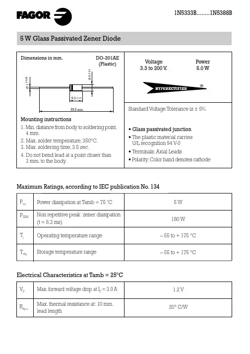
·Voltage Range 8.2V - 200V ·Glass Passivated Junction ·5W Steady State·High Surge Capability·±5% Voltage Tolerance on Nominal V Z is Standard ·100% Tested1N5344B - 1N5388B5W ZENER DIODENotes:1.Nominal Zener Voltage (V Z ) is read with the device in standard test clips with 3/8- to 1/2-inch spacing between clip and case of the diode. Before reading, the diode is allowed to stabilize for a period of 40 ±10 milliseconds at 25°C +8, -2°C.2.The Zener Impedance (Z Zor Z ZK ) is derived from the 60 Hz ac voltage, which results when an ac current having an rmsvalue equal to 10% of the dc zener current (I ZT or I ZK ) is superimposed on I ZT or I ZK, respectively.3.The Surge Current (I ZSM ) is specified as the maximum peak of a nonrecurrent sine wave of 8.3 milliseconds duration.4.Voltage regulation (D V Z ) is the difference between the voltage measured at 10% and 50% of I ZM .Maximum Ratings@ T A= 25°C unless otherwise specifiedFeaturesMechanical Data·Case: Molded Plastic Over Glass Passivated Junction·Leads: Solderable per MIL-STD-202,Method 208·Polarity: Cathode Band ·Approx. Weight: 1.2 gramsElectrical Characteristics@ T A = 25°C unless otherwise specifiedV F = 1.2V max at I F = 1.0A all types.Suffix ‘B’ denotes 5% tolerance which is standard.11010010000.11.010100V ,REVERSE VOLTAGE (V)R Fig.1, Typ.Capacitance vs.Reverse VoltageC ,C A P A C I T A N C E (p F )j123456255075100125150175200T LEAD TEMPERATURE 9.5mm FROM BODY (ºC)L,Fig.3,Power Derating CurveP ,P O W E R D I S S I P A T I O N (W )d 1.0101001000I ,ZENER CURRENT (mA)ZT Fig.2,Typ.Zener Impedance vs.Zener CurrentZ ,Z E N E R I M P E D A N C E (W )Z T。
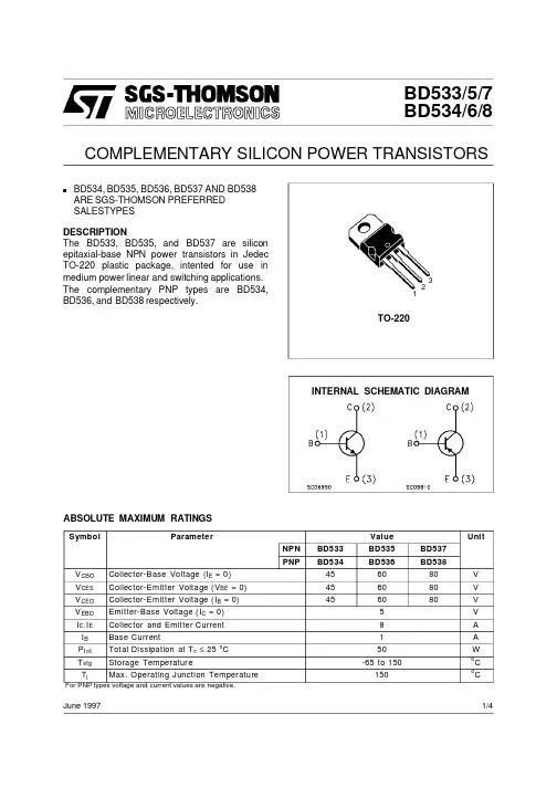
BD533/5/7BD534/6/8COMPLEMENTARY SILICON POWER TRANSISTORSsBD534,BD535,BD536,BD537AND BD538ARE SGS-THOMSON PREFERRED SALESTYPESDESCRIPTIONThe BD533,BD535,and BD537are silicon epitaxial-base NPN power transistors in Jedec TO-220plastic package,intented for use in medium power linear and switching applications.The complementary PNP types are BD534,BD536,and BD538respectively.INTERNAL SCHEMATIC DIAGRAMJune 1997ABSOLUTE MAXIMUM RATINGSSymbolParameterValueUnitNPN BD533BD535BD537PNPBD534BD536BD538V CBO Collector-Base Voltage (I E =0)456080V V CES Collector-Emitter Voltage (V BE =0)456080V V CEO Collector-Emitter Voltage (I B =0)456080V V EBO Emitter-Base Voltage (I C =0)5V I C,I E Collector and Emitter Current 8A I B Base Current1A P t ot Total Dissipation at T c ≤ 25 oC 50WT stg Storage Temperature-65to 150o C T jMax.Operating Junction Temperature150oCFor PNP types voltage and current values are negative.123TO-2201/4THERMAL DATAR t hj-ca se R t hj-amb Thermal Resistance Junction-case MaxThermal Resistance Junction-ambient Max2.570o C/Wo C/WELECTRICAL CHARACTERISTICS(T case=25o C unless otherwise specified)Symbol Parameter Test Conditions Min.Typ.Max.UnitI CBO Collector Cut-offCurrent(I E=0)for BD533/534V CB=45Vfor BD535/536V CB=60Vfor BD537/538V CB=80V100100100µAµAµAI CES Collector Cut-offCurrent(V BE=0)for BD533/534V CE=45Vfor BD535/536V CE=60Vfor BD537/538V CE=80V100100100µAµAµAI EBO Emitter Cut-off Current(I C=0)V EB=5V1mAV CEO(sus)∗Collector-EmitterSustaining Voltage(I B=0)I C=100mA for BD533/534for BD535/536for BD537/538456080VVVV CE(sat)∗Collector-EmitterSaturation Voltage I C=2A I B=0.2AI C=6A I B=0.6A0.80.8VVV BE∗Base-Emitter Voltage I C=2A V CE=2V 1.5V h FE∗DC Current Gain I C=10mA V CE=5Vfor BD533/534for BD535/536for BD537/538 I C=500mA V CE=2VI C=2A V CE=2Vfor BD533/534for BD535/536for BD537/53820 20 15 40 25 25 15f T Transition frequency I C=500mA V CE=1V312MHz ∗ Pulsed:Pulse duration=300µs,duty cycle1.5%For PNP types voltage and current values are negative.Safe Operating AreasBD533/BD534/BD535/BD536/BD537/BD5382/4DIM.mminch MIN.TYP.MAX.MIN.TYP.MAX.A 4.40 4.600.1730.181C 1.23 1.320.0480.051D 2.402.720.0940.107D1 1.270.050E 0.490.700.0190.027F 0.610.880.0240.034F1 1.14 1.700.0440.067F2 1.14 1.700.0440.067G 4.95 5.150.1940.203G1 2.4 2.70.0940.106H210.010.400.3930.409L216.40.645L413.014.00.5110.551L5 2.65 2.950.1040.116L615.2515.750.6000.620L7 6.2 6.60.2440.260L9 3.5 3.930.1370.154DIA.3.75 3.850.1470.151P011CTO-220MECHANICAL DATABD533/BD534/BD535/BD536/BD537/BD5383/4BD533/BD534/BD535/BD536/BD537/BD538Information furnished is believed to be accurate and reliable.However,SGS-THOMSON Microelectronics assumes no responsability for the consequences of use of such information nor for any infringementof patents or other rights of third parties which may results from its use.No license is granted by implication or otherwise under any patent or patent rights of SGS-THOMSON Microelectronics.Specifications mentioned in this publication are subject to change without notice.This publicationsupersedes and replaces all information previously supplied.SGS-THOMSON Microelectronics products are notauthorized for use as critical components in life support devices or systems without express written approval of SGS-THOMSON Microelectonics.©1997SGS-THOMSON Microelectronics-Printed in Italy-All Rights ReservedSGS-THOMSON Microelectronics GROUP OF COMPANIESAustralia-Brazil-Canada-China-France-Germany-Hong Kong-Italy-Japan-Korea-Malaysia-Malta-Morocco-The Netherlands-Singapore-Spain-Sweden-Switzerland-Taiwan-Thailand-United Kingdom-U.S.A...4/4。
350V NPN HIGH VOLTAGE TRANSISTOR IN SOT23Features∙ BV CEO > 350V∙ I C = 500mA High Collector Current ∙ 350mW Power Dissipation ∙ h FE of 15 @ I C =100mA∙ Complementary Part Number: FMMT6520∙ Totally Lead-Free & Fully RoHS Compliant (Notes 1 & 2) ∙ Halogen and Antimony Free. “Green” Device (Note 3) ∙ Qualified to AEC-Q101 Standards for High ReliabilityMechanical Data∙ Case: SOT23∙ Case Material: Molded Plastic. “Green” Molding Compound. UL Flammability Classification Rating 94V-0 ∙ Moisture Sensitivity: Level 1 per J-STD-020∙ Terminals: Finish - Matte Tin Plated Leads, Solderable per MIL-STD-202, Method 208∙ Weight: 0.008 grams (Approximate)2. See https:///quality/lead-free/ for more information about Diodes Incorporated’s definitions of Halogen - and Antimony-free, "Green" andLead-free.3. Halogen- and Antimony-free "Green” products are defined as those which contain <900ppm bromine, <900ppm chlorine (<1500ppm total Br + Cl) and<1000ppm antimony compounds.4. For packaging details, go to our website at https:///design/support/packaging/diodes-packaging/.Marking Information517 = Product Type Marking CodeSOT23Top View Pin-OutTop ViewDevice Symbol517SOT23CEBThermal Characteristics(@T A = +25°C, unless otherwise specified.)ESD Ratings (Note 8)Notes: 5. For the device mounted on minimum recommended pad layout 1oz copper that is on a single-sided 1.6mm FR-4 PCB; device is measured under still air conditions whilst operating in steady state condition.6. Same as note (5), except the device is mounted on 15mm x 15mm 1oz copper.7. Thermal resistance from junction to solder-point (at the end of the leads).8. Refer to JEDEC specification JESD22-A114 and JESD22-A115.Thermal Characteristics and Derating informationPulse Width (s)Pulse Power DissipationElectrical Characteristics(@T A = +25°C, unless otherwise specified.)Note: 9. Measured under pulsed conditions. Pulse width ≤300µs. Duty cycle ≤ 2%.Typical Electrical Characteristics (@T A = +25°C, unless otherwise specified.)VCE(SAT)v ICVCE(SAT)(V)ICCollector Current (mA)VBE(SAT)v ICVCE(SAT)(V)ICCollector Current (mA)hFEv ICTypicalGain(hFE)ICCollector Current (mA)VCE(SAT)v ICVBE(SAT)(V)ICCollector Current (mA)VBE(ON)v ICVBE(ON)(V)ICCollector Current (mA)Package Outline DimensionsPlease see /package-outlines.html for the latest version.SOT23Suggested Pad LayoutPlease see /package-outlines.html for the latest version.SOT23Note:For high voltage applications, the appropriate industry sector guidelines should be considered with regards to creepage and clearance distances between device Terminals and PCB tracking.。
T-18APPLICATIONS / BENEFITS Regulates voltage over a broad operating current andNOTE 1: Devices listed above with B suffix have ±5% tolerance, A suffix designates ±10% tolerance, C suffix designates ±2% tolerance, and D suffix designates ±1% tolerance. No suffix designates ±20%.2: Zener voltage (Vz) is measured at T L = 25o C (+8, -2o C). Voltage measurement performed at 40 ±10 millisecondsNOTEafter application of dc current.3: The zener impedance is derived from 1 kHz ac voltage resulting from an ac current modulation having an rms valueNOTEequal to 10% of the dc zener current (I ZT or I ZK) superimposed on I ZT or I ZK. See Micro Note 202 for zener impedancevariation with different operating currents.4: The maximum current (I ZM) shown is for a ±5% tolerance devices. The I ZM for other tolerances can be calculated using NOTEthe formula: I ZM = P/V ZM where V ZM is the V Z at the high end of the voltage tolerance specified and P is the rated power for the method of mounting.NOTE5: The surge current (I ZSM) is specified as the maximum peak of a non-recurrent half-sine wave of 8.3 ms duration.NOTE 6: Voltage regulation (∆V Z)is the difference between the voltage measured at 10% and 50% of I ZM.T LT A on FR4 PC boardLT A ambient temperature on FR4 PC BoardFIGURE 1FIGURE 2Power Derating Curve Typical Capacitance vs.Reverse Voltage for 5 Watt ZenersFIGURE 3PACKAGE DIMENSIONSTypical Capacitance vs.Reverse Voltage for 5 Watt Zeners。
UG462: Si5332-12A-EVB User's Guide (Using Si5332-AM3-QFN48-EVB)The Si5332-AM3-QFN48-EVB is used for evaluating the twelve output Automotive grade Si5332 Low Jitter Any-Frequency Clock Generator. The Si5332-AM3 device uses the patented Multisynth™ technology to generate up to twelve independent clock frequen-cies each with 0 ppm synthesis error. The Si5332-AM3-QFN48-EVB can use the on-board 25 MHz crystal as a reference or one of three independent input reference clocks.The Si5332-AM3-QFN48-EVB can be controlled and configured using the SkyworksClock Builder Pro™ (CBPro™) software tool.EVB FEATURES•Powered from either USB port or external +5 V power supply•25 MHz crystal reference or external input clock reference•Programmable device VDD supply for operation at 3.3 V, 2.5 V, or 1.8 V,controlled by CBPro software•Programmable VDDO supplies allow each of the 6 clock output banks to have its own power supply voltage selectable from 3.3V, 2.5 V, 1.8 V or 1.5 V (1.5 V LVCMOS only)•CBPro GUI-controlled voltage, current, and power measurements of VDD and all VDDO supplies•SMA connectors for all input and output clocks•External digital input functions emulated via on-board switchesTable of Contents1. Functional Block Diagram (3)2. Si5332 CBPro Overview (4)3. Si5332-AM3-QFN48-EVB (5)3.1 Initial Default Configuration (5)3.2 DIP Switch Functions (6)3.3 LEDs (6)3.4 Input Clocks (7)3.5 Output Clocks (8)4. Using CBPro with Si5332-AM3-QFN48-EVB (9)4.1 CBPro EVB GUI (10)4.2 Device Register Changes using the CBPro EVB GUI (11)4.3 Creating a New Si5332-AM3 CBPro Configuration (12)5. Si5332-AM3-QFN48-EVB Rev 1.0 Schematics (14)UG462: Si5332-12A-EVB User's Guide (Using Si5332-AM3-QFN48-EVB) • Functional Block Diagram1. Functional Block DiagramBelow is a functional block diagram of the Si5332-AM3-QFN48-EVB. This EVB can be connected to a PC via the main USB connector for configuration, control, and monitoring using Skyworks’ CBPro software. The EVB’s power can be supplied from the USB connection or external +5 V power source.Figure 1.1. Si5332-AM3-QFN48-EVB Functional Block Diagram2. Si5332 CBPro OverviewAll Si5332 devices, and corresponding EVBs, are fully supported in Skyworks’ ClockBuilder Pro (CBPro) software. Note that CBPro software is required to configure and use the Si5332-AM3-QFN48-EVB. Download and install CBPro from here.With CBPro, users can perform the following:1.Create full device configurations (frequency plans) including multi-profile configurations.2.Get estimated power consumption and estimated operating junction temperature of your configuration.3.Evaluate/Test configurations using a supported EVB.4.Create downloadable configuration files designed to be I2C downloaded into target Si5332 device.5.Submit a configuration for creation of a custom, factory-programmed device with a unique orderable part number (no added cost).6.Submit a request for a phase noise report of your specific configuration.Figure 2.1. CBPro Start-up Window3. Si5332-AM3-QFN48-EVB3.1 Initial Default ConfigurationThe Si5332-AM3-QFN48-EVB has power supply configuration DIP switches (SW1 – SW7), which are set at the factory to the OFF position. The EVB also has a programmable digital input (GPIO) configuration DIP switch (SW10), also with all switches set to OFF position. The required EVB default DIP switch settings are all switched OFF (as shown below) and these settings are required to allow CBPro software to control and configure the EVB. In addition, JP1 jumper should be installed on “USB” side (pins 1 & 2).Figure 3.1. EVB Default DIP Switch Settings in the OFF Position3.2 DIP Switch FunctionsThe power supply DIP switches (SW1 – SW7) are intended to provide flexibility in cases when a pre-programmed Si5332-AM3 device is installed on the board and CBPro will not be used to configure the Si5332-AM3 device or to control the on-board power supply settings. Typically, the power supply DIP switches (SW1- SW7) will only be used if a configuration is burned into the Si5332-AM3’s NVM by using the CBPro Field Programming Dongle or a if pre-configured Si5332-AM3 (custom OPN) is installed on the EVB.The programmable digital input (GPIO) signal configuration switch (SW10) will only be used to turn specific features on/off based on the CBPro configuration loaded into the Si5332-AM3 device. For example, a programmable digital input, such as an Output Enable (OE), can be assigned to Input 1. Once the Si5332-AM3 configuration with Input 1 assigned as OE is loaded, Input 1 on SW10 can be used to control this OE input signal by setting high/low. Input 1 switch OFF = 1, Input 1 switch ON = 0.3.3 LEDsThe Si5332-AM3-QFN48-EVB has three indicator LEDs (D2, D3, D4) near the USB connector as shown and defined below.Figure 3.2. Si5332-AM3-QFN48-EVB LED LocationsD2: This Blue LED (+5VUSB) lights to indicate USB +5 V is present.D3: This Green LED (Ready) lights to indicate the EVB’s USB has enumerated with the host PC.D4: This Green LED (Busy) lights to indicate CBPro has successfully connected to the EVB.The Si5332-AM3 device can support three sources of input from the reference clock. One source is the crystal input on XA/XB pins (XA can also be used as a single-ended external input if the crystal is removed, see the Si5332-AM3 data sheet for more details.). The other two are separate external input clock sources which can be either differential or single-ended clocks.As shown in the schematic below, the Si5332-AM3-QFN48-EVB is pre-populated with a 25 MHz crystal on the XA/XB crystal input. Both differential external clock inputs have 50 Ω terminations installed by default. The CLKIN1 input has “not-installed” (“NI”) compo-nents to isolate the CLKIN1 input from the crystal circuit when the crystal is installed.Figure 3.3. Si5332-AM3-QFN48-EVB Input Clock CircuitThe Si5332-AM3 device can support up to 12 differential pair outputs or 12 pairs of LVCMOS outputs (24 total LVCMOS outputs). Each output pair has an output termination circuit as shown in figure below. The default output termination is AC-coupled outputs from Si5332-AM3 device with no other termination.The default output termination components (0 Ω and 0.1 µF) combined with the “NI” (not installed) component sites on the EVB can be used as locations to create the desired output termination configuration. For example, if dc output termination is required, the 0.1 µF caps can be replaced with 0 Ω resistors. Note that not all possible termination schemes can be supported by the circuit below and in some cases external components may be required.Figure 3.4. Si5332-AM3-QFN48-EVB Single Pair Output Clock Termination Circuit4. Using CBPro with Si5332-AM3-QFN48-EVBSkyworks’ CBPro software is required for using the Si5332-AM3-QFN48-EVB. It can be downloaded from this Skyworks website link: https:///en/Application-Pages/Clockbuilder-Pro-SoftwareOnce downloaded and installed, running CBPro should present the following window:Figure 4.1. CBPro Opening WindowIf an evaluation board is connected via USB, the EVB will be detected as shown next to the arrow in the image above. Multiple EVBs can be connected and individually selected in CBPro.The EVB GUI is a useful tool as it allows monitoring and control of EVB functions such as digital inputs, power supply voltage, and current measurements. The EVB GUI can also be used to read and write on-chip registers and report other useful status information.4.1 CBPro EVB GUIThe EVB GUI is invoked by pressing the “EVB GUI” button from CBPro’s main window. A new EVB GUI window will be opened, as shown below. Across the top are several tabs for selecting various useful informational pages, and pages for configuration, control, or monitoring of the EVB.Figure 4.2. EVB GUI - Info PageThe “Info” tab shows information regarding the EVB board and DUT device identification. Both the “Control Registers” and “Log”windows are shown in all EVB GUI tabs. The “Control Registers” are useful buttons to place the Si5332 device in Active or Ready mode or to reset the device. Refer to the “Status Registers” tab for important information on device modes and their effects on register accesses. The “Log” window is a log of all CBPro EVB communications.The “DUT Settings Editor” and “DUT Register Editor” tabs allow registers to be read/written by either the setting name or by direct hex byte access.Figure 4.3. EVB GUI - DUT Settings / DUT Register EditorsThe “Regulators” tab allows reading the voltages and currents for each on-board power supply. Each regulator may be switched on/off or have the voltage changed as necessary. Similarly, the “GPIO” tab allows for monitoring and control of the Si5332 programmable digital inputs.Figure 4.4. EVB GUI – Regulators and GPIO Monitoring/Control4.2 Device Register Changes using the CBPro EVB GUIThe last EVB GUI tab is the “Status Registers” tab, which shows the present state of the device in either “Active” or “Ready” mode. Note: The Si5332 device must be in “Active” mode to output any clocks. While in “Active” mode, most register write accesses will not be allowed and will be blocked by the device. The device must be in “Ready” mode to allow write access to many registers. While the device is in “Ready” mode, the outputs are stopped. Once the device is placed back in “Active” mode, the outputs will resume based on any register changes done while in “Ready” mode.The only registers not requiring this process are Spread Spectrum enable/disable, Output Enable controls, Input Clock Selection, and the register controlling placement of the device into and out of Active or Ready mode. Do not rely on the device being in “Active” mode to prevent inadvertent I2C write cycles from corrupting device registers.The general process required to change register values (i.e., register writes) is shown below.1.Place the device into “Ready” mode, at which time the outputs will stop and register changes can be made.a.Press “Ready Mode” button, then “Refresh All” button to update Status.b.Confirm device is in “Ready” mode.2.Perform any register updates as desired.3.Place device back into “Active” mode for the register changes to take effect and to enable outputs.a.Press “Active Mode” button, then “Refresh All” button to update Status.b.Confirm device is now in “Active” mode.4.3 Creating a New Si5332-AM3 CBPro Configuration1.To start a new Si5332-AM3 project, click on “Create New Project” from the CBPro opening window.2.From the selection window, click on “Clock Generators”.3.Next, select Si5332-GM3/AM3 from the list of devices.plete the guided step-by-step configuration process, making sure to select Automotive grade in Step 3.5.When you have completed all steps, press the “Write to EVB” button to download your configuration to the connected EVB. Your configuration now should be actively running in the Si5332-AM3-QFN48-EVB.5. Si5332-AM3-QFN48-EVB Rev 1.0 SchematicsThe Si5332-AM3-QFN48-EVB schematic, BOM, and layout information can be found at the following link: https:///search?doc=Schematics%20and%20Layouts#documentsCopyright © 2021 Skyworks Solutions, Inc. All Rights Reserved.Information in this document is provided in connection with Skyworks Solutions, Inc. (“Skyworks”) products or services. These materials, including the information contained herein, are provided by Skyworks as a service to its customers and may be used for informational purposes only by the customer. Skyworks assumes no responsibility for errors or omissions in these materials or the information contained herein. Skyworks may change its documentation, products, services, specifications or product descriptions at any time, without notice. Skyworks makes no commitment to update the materials or information and shall have no responsibility whatsoever for conflicts, incompatibilities, or other difficulties arising from any future changes.No license, whether express, implied, by estoppel or otherwise, is granted to any intellectual property rights by this document. Skyworks assumes no liability for any materials, products or information provided hereunder, including the sale, distribution, reproduction or use of Skyworks products, information or materials, except as may be provided in Skyworks’ Terms and Conditions of Sale.THE MATERIALS, PRODUCTS AND INFORMATION ARE PROVIDED “AS IS” WITHOUT WARRANTY OF ANY KIND, WHETHER EXPRESS, IMPLIED, STATUTORY, OR OTHERWISE, INCLUDING FITNESS FOR A PARTICULAR PURPOSE OR USE, MERCHANTABILITY, PERFORMANCE, QUALITY OR NON-INFRINGEMENT OF ANY INTELLECTUAL PROPERTY RIGHT; ALL SUCH WARRANTIES ARE HEREBY EXPRESSLY DISCLAIMED. SKYWORKS DOES NOT WARRANT THE ACCURACY OR COMPLETENESS OF THE INFORMATION, TEXT, GRAPHICS OR OTHER ITEMS CONTAINED WITHIN THESE MATERIALS. SKYWORKS SHALL NOT BE LIABLE FOR ANY DAMAGES, INCLUDING BUT NOT LIMITED TO ANY SPECIAL, INDIRECT, INCIDENTAL, STATUTORY, OR CONSEQUENTIAL DAMAGES, INCLUDING WITHOUT LIMITATION, LOST REVENUES OR LOST PROFITS THAT MAY RESULT FROM THE USE OF THE MATERIALS OR INFORMATION, WHETHER OR NOT THE RECIPIENT OF MATERIALS HAS BEEN ADVISED OF THE POSSIBILITY OF SUCH DAMAGE.Skyworks products are not intended for use in medical, lifesaving or life-sustaining applications, or other equipment in which the failure of the Skyworks products could lead to personal injury, death, physical or environmental damage. Skyworks customers using or selling Skyworks products for use in such applications do so at their own risk and agree to fully indemnify Skyworks for any damages resulting from such improper use or sale.Customers are responsible for their products and applications using Skyworks products, which may deviate from published specifications as a result of design defects, errors, or operation of products outside of published parameters or design specifications. Customers should include design and operating safeguards to minimize these and other risks. Skyworks assumes no liability for applications assistance, customer product design, or damage to any equipment resulting from the use of Skyworks products outside of Skyworks’ published specifications or parameters.Skyworks, the Skyworks symbol, Sky5®, SkyOne ®, SkyBlue™, Skyworks Green™, Clockbuilder ®, DSPLL ®, ISOmodem ®, ProSLIC ®, and SiPHY ® are trademarks or registered trademarks of Skyworks Solutions, Inc. or its subsidiaries in the United States and other countries. Third-party brands and names are for identification purposes only and are the property of their respective owners. Additional information, including relevant terms and conditions, posted at , are incorporated by reference.Portfolio/ia/timing SW/HW /CBPro Quality /quality Support & Resources /support ClockBuilder ProCustomize Skyworks clock generators,jitter attenuators and networksynchronizers with a single tool. WithCBPro you can control evaluationboards, access documentation, requesta custom part number, export for in-system programming and more!/CBPro。