CY23EP05SXC-1中文资料
- 格式:pdf
- 大小:399.22 KB
- 文档页数:12
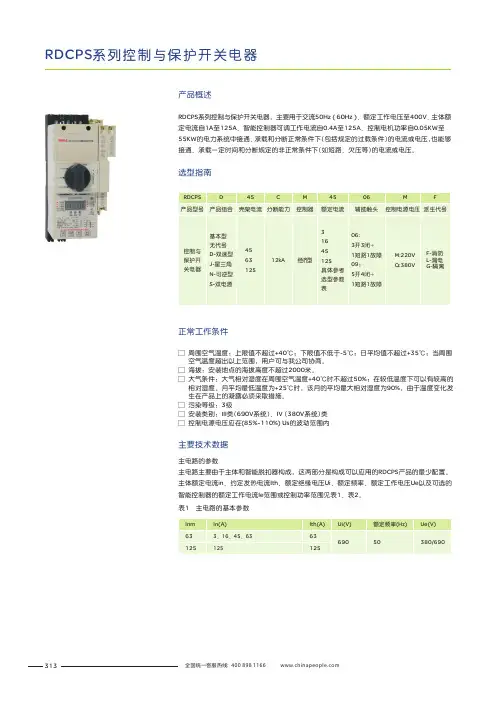
313RDCPS 系列控制与保护开关电器RDCPS 系列控制与保护开关电器,主要用于交流50Hz ( 60Hz )、额定工作电压至400V 、主体额定电流自1A 至125A 、智能控制器可调工作电流自0.4A 至125A 、控制电机功率自0.05KW 至55KW 的电力系统中接通、承载和分断正常条件下(包括规定的过载条件)的电流或电压,也能够接通、承载一定时间和分断规定的非正常条件下(如短路、欠压等)的电流或电压。
□ 周围空气温度:上限值不超过+40℃;下限值不低于-5℃;日平均值不超过+35℃;当周围 空气温度超出以上范围,用户可与我公司协商。
□ 海拔:安装地点的海拔高度不超过2000米。
□ 大气条件:大气相对湿度在周围空气温度+40℃时不超过50%;在较低温度下可以有较高的 相对湿度。
月平均最低温度为+25℃时,该月的平均最大相对湿度为90%,由于温度变化发 生在产品上的凝露必须采取措施。
□ 污染等级:3级□ 安装类别:III 类(690V 系统)、IV (380V 系统)类□ 控制电源电压应在(85%~110%) Us 的波动范围内正常工作条件产品概述选型指南主电路的参数主电路主要由于主体和智能脱扣器构成,这两部分是构成可以应用的RDCPS 产品的最少配置。
主体额定电流in 、约定发热电流Ith 、额定绝缘电压Ui 、额定频率、额定工作电压Ue 以及可选的智能控制器的额定工作电流Ie 范围或控制功率范围见表1、表2。
主要技术数据表1主电路的基本参数314注:□ 瞬时保护参数li 不可调,其值整定在16le电机用产品其短延时保护整定参数ls 可调范围为6lr~12lr □ □ 配电用产品其短延时保护整定参数Is 可调范围为3lr~6lr □ 以上功率范围参考Y 系列三相异步电动机的技术参数 □如有特殊要求时请生产厂家联系表2 主电路的主要参数315RDCPS 系列控制与保护开关电器RDCPS保护特性曲线1.0l r 1最小1.2l r 1最小1.0l r 1最大1.2l r 1最大6l r 1(l r 2最小)12l r 1(l r 2最16l r 1±1520l r 1±20I c s I(A)RDCPS电动机保护时间-电流特性0.1s 0.01s 0.001s1.05l r 1最小1.30l r 1最小1.05l r 1最大1.30l r 1最大3l r 1(l r 2最小)6l r 1(l r 2最大)16l r 1±1520l n ±20%I c sI(A)RDCPS 配电保护时间-电流特性用于电动机控制(使用类别:AC-42、AC-43、AC-44)的动作特性316智能脱扣器主要技术参数□ 起动延时在RDCPS 起动时间内,只对缺相、断相、过压、欠压、欠流、短路、漏电及三相不平衡进行保护,以避免RDCPS 启动大电流和过电流的保护;整定时间为 ( 1~99 ) 秒内之间选择;□ 过压及欠压保护只对辅助电源电压进行保护,以确保线圈与智能控制器正常工作;过压保护:当辅助电源电压超过设定值时(出厂整定在120%Us ),动作时间≤10秒;欠压保护:当辅助电源电压低于设定值时(出厂整定在85%Us ),动作时间≤10秒;□ 反时限过载长延时保护用户根据负载电流I 设定智能脱扣器的额定工作电流Ie ,使负载电流I 在80~100%Ie 之间,动作时间应根据负载特性设定,过流倍数与动作时间特性见表四,反时限过载长延时保护特性曲线出厂设定在F1表3 RDCPS反时限过载长延时保护动作特性用于配电线路负载(使用类别:AC-40、AC-41)的动作特性□ 欠流保护欠流保护:是根据最小电流与额定电流的比值来判断是否启动欠流保护(出厂设定在0),可以对不能空载的电机进行保护;也可以避免用户未根据负载电流I 设定RDCPS 智能脱扣器的工作电流Ie ,从而导致电机不在RDCPS 的保护范围内。
元器件交易网CY7C63743CY7C63722/23CY7C63743enCoRe™ USBCombination Low-Speed USB & PS/2Peripheral ControllerTABLE OF CONTENTS1.0 FEATURES (5)2.0 FUNCTIONAL OVERVIEW (6)2.1 enCoRe USB - The New USB Standard (6)3.0 LOGIC BLOCK DIAGRAM (7)4.0 PIN CONFIGURATIONS (7)5.0 PIN ASSIGNMENTS (7)6.0 PROGRAMMING MODEL (8)6.1 Program Counter (PC) (8)6.2 8-bit Accumulator (A) (8)6.3 8-bit Index Register (X) (8)6.4 8-bit Program Stack Pointer (PSP) (8)6.5 8-bit Data Stack Pointer (DSP) (9)6.6 Address Modes (9)6.6.1 Data (9)6.6.2 Direct (9)6.6.3 Indexed (9)7.0 INSTRUCTION SET SUMMARY (10)8.0 MEMORY ORGANIZATION (11)8.1 Program Memory Organization (11)8.2 Data Memory Organization (12)8.3 I/O Register Summary (13)9.0 CLOCKING (14)9.1 Internal/External Oscillator Operation (15)9.2 External Oscillator (16)10.0 RESET (16)10.1 Low-voltage Reset (LVR) (16)10.2 Brown Out Reset (BOR) (16)10.3 Watchdog Reset (WDR) (17)11.0 SUSPEND MODE (17)11.1 Clocking Mode on Wake-up from Suspend (18)11.2 Wake-up Timer (18)12.0 GENERAL PURPOSE I/O PORTS (18)12.1 Auxiliary Input Port (21)13.0 USB SERIAL INTERFACE ENGINE (SIE) (22)13.1 USB Enumeration (22)13.2 USB Port Status and Control (22)14.0 USB DEVICE (24)14.1 USB Address Register (24)14.2 USB Control Endpoint (24)14.3 USB Non-control Endpoints (25)14.4 USB Endpoint Counter Registers (26)15.0 USB REGULATOR OUTPUT (27)16.0 PS/2 OPERATION (27)17.0 SERIAL PERIPHERAL INTERFACE (SPI) (28)17.1 Operation as an SPI Master (29)17.2 Master SCK Selection (29)17.3 Operation as an SPI Slave (29)17.4 SPI Status and Control (30)17.5 SPI Interrupt (31)17.6 SPI Modes for GPIO Pins (31)18.0 12-BIT FREE-RUNNING TIMER (31)19.0 TIMER CAPTURE REGISTERS (32)20.0 PROCESSOR STATUS AND CONTROL REGISTER (35)21.0 INTERRUPTS (36)21.1 Interrupt Vectors (37)21.2 Interrupt Latency (37)21.3 Interrupt Sources (37)22.0 USB MODE TABLES (42)23.0 REGISTER SUMMARY (47)24.0 ABSOLUTE MAXIMUM RATINGS (48)25.0 DC CHARACTERISTICS (48)26.0 SWITCHING CHARACTERISTICS (50)27.0 ORDERING INFORMATION (55)28.0 PACKAGE DIAGRAMS (55)LIST OF FIGURESFigure 8-1. Program Memory Space with Interrupt Vector Table (11)Figure 8-2. Data Memory Organization (12)Figure 9-1. Clock Oscillator On-chip Circuit (14)Figure 9-2. Clock Configuration Register (Address 0xF8) (14)Figure 10-1. Watchdog Reset (WDR, Address 0x26) (17)Figure 12-1. Block Diagram of GPIO Port (one pin shown) (19)Figure 12-2. Port 0 Data (Address 0x00) (19)Figure 12-3. Port 1 Data (Address 0x01) (19)Figure 12-4. GPIO Port 0 Mode0 Register (Address 0x0A) (20)Figure 12-5. GPIO Port 0 Mode1 Register (Address 0x0B) (20)Figure 12-6. GPIO Port 1 Mode0 Register (Address 0x0C) (20)Figure 12-7. GPIO Port 1 Mode1 Register (Address 0x0D) (20)Figure 12-8. Port 2 Data Register (Address 0x02) (21)Figure 13-1. USB Status and Control Register (Address 0x1F) (23)Figure 14-1. USB Device Address Register (Address 0x10) (24)Figure 14-2. Endpoint 0 Mode Register (Address 0x12) (25)Figure 14-3. USB Endpoint EP1, EP2 Mode Registers (Addresses 0x14 and 0x16) (26)Figure 14-4. Endpoint 0,1,2 Counter Registers (Addresses 0x11, 0x13 and 0x15) (26)Figure 17-1. SPI Block Diagram (28)Figure 16-1. Diagram of USB-PS/2 System Connections (28)Figure 17-2. SPI Data Register (Address 0x60) (29)Figure 17-3. SPI Control Register (Address 0x61) (30)Figure 17-4. SPI Data Timing (31)Figure 18-1. Timer LSB Register (Address 0x24) (31)Figure 18-2. Timer MSB Register (Address 0x25) (32)Figure 18-3. Timer Block Diagram (32)Figure 19-1. Capture Timers Block Diagram (33)Figure 19-2. Capture Timer A-Rising, Data Register (Address 0x40) (33)Figure 19-3. Capture Timer A-Falling, Data Register (Address 0x41) (34)Figure 19-4. Capture Timer B-Rising, Data Register (Address 0x42) (34)Figure 19-5. Capture Timer B-Falling, Data Register (Address 0x43) (34)Figure 19-6. Capture Timer Status Register (Address 0x45) (34)Figure 19-7. Capture Timer Configuration Register (Address 0x44) (34)Figure 20-1. Processor Status and Control Register (Address 0xFF) (35)Figure 21-1. Global Interrupt Enable Register (Address 0x20) (38)Figure 21-2. Endpoint Interrupt Enable Register (Address 0x21) (39)Figure 21-3. Interrupt Controller Logic Block Diagram (40)Figure 21-4. Port 0 Interrupt Enable Register (Address 0x04) (40)Figure 21-5. Port 1 Interrupt Enable Register (Address 0x05) (40)Figure 21-6. Port 0 Interrupt Polarity Register (Address 0x06) (41)Figure 21-7. Port 1 Interrupt Polarity Register (Address 0x07) (41)Figure 21-8. GPIO Interrupt Diagram (41)Figure 26-1. Clock Timing (51)Figure 26-2. USB Data Signal Timing (51)Figure 26-3. Receiver Jitter Tolerance (52)Figure 26-4. Differential to EOP Transition Skew and EOP Width (52)Figure 26-5. Differential Data Jitter (52)Figure 26-7. SPI Slave Timing, CPHA = 0 (53)Figure 26-6. SPI Master Timing, CPHA = 0 (53)Figure 26-8. SPI Master Timing, CPHA = 1 (54)Figure 26-9. SPI Slave Timing, CPHA = 1 (54)LIST OF TABLESTable 8-1. I/O Register Summary (13)Table 11-1. Wake-up Timer Adjust Settings (18)Table 12-1. Ports 0 and 1 Output Control Truth Table (21)Table 13-1. Control Modes to Force D+/D– Outputs (24)Table 17-1. SPI Pin Assignments (31)Table 19-1. Capture Timer Prescalar Settings (Step size and range for FCLK = 6 MHz) (35)Table 21-1. Interrupt Vector Assignments (37)Table 22-1. USB Register Mode Encoding for Control and Non-Control Endpoints (42)Table 22-2. Decode table for Table 22-3: “Details of Modes for Differing Traffic Conditions” (44)Table 22-3. Details of Modes for Differing Traffic Conditions (45)Table 28-1. CY7C63722-XC Probe Pad Coordinates in microns ((0,0) to bond pad centers) (57)1.0 Features•enCoRe™ USB - enhanced Component Reduction—Internal oscillator eliminates the need for an external crystal or resonator—Interface can auto-configure to operate as PS/2 or USB without the need for external components to switch between modes (no GPIO pins needed to manage dual mode capability)—Internal 3.3V regulator for USB pull-up resistor—Configurable GPIO for real-world interface without external components•Flexible, cost-effective solution for applications that combine PS/2 and low-speed USB, such as mice, gamepads, joysticks, and many others.•USB Specification Compliance—Conforms to USB Specification, Version 2.0—Conforms to USB HID Specification, Version 1.1—Supports 1 Low-Speed USB device address and 3 data endpoints—Integrated USB transceiver—3.3V regulated output for USB pull-up resistor•8-bit RISC microcontroller—Harvard architecture—6-MHz external ceramic resonator or internal clock mode—12-MHz internal CPU clock—Internal memory—256 bytes of RAM—8 Kbytes of EPROM—Interface can auto-configure to operate as PS/2 or USB—No external components for switching between PS/2 and USB modes—No GPIO pins needed to manage dual mode capability•I/O ports—Up to 16 versatile General Purpose I/O (GPIO) pins, individually configurable—High current drive on any GPIO pin: 50 mA/pin current sink—Each GPIO pin supports high-impedance inputs, internal pull-ups, open drain outputs or traditional CMOS outputs —Maskable interrupts on all I/O pins•SPI serial communication block—Master or slave operation—2 Mbit/s transfers•Four 8-bit Input Capture registers—Two registers each for two input pins—Capture timer setting with 5 prescaler settings—Separate registers for rising and falling edge capture—Simplifies interface to RF inputs for wireless applications•Internal low-power wake-up timer during suspend mode—Periodic wake-up with no external components•Optional 6-MHz internal oscillator mode—Allows fast start-up from suspend mode•Watchdog Reset (WDR)•Low-voltage Reset at 3.75V•Internal brown-out reset for suspend mode•Improved output drivers to reduce EMI•Operating voltage from 4.0V to 5.5VDC•Operating temperature from 0 to 70 degrees Celsius•CY7C63723 available in 18-pin SOIC, 18-pin PDIP•CY7C63743 available in 24-pin SOIC, 24-pin PDIP•CY7C63722 available in DIE form•Industry standard programmer support2.0 Functional Overview2.1enCoRe USB - The New USB StandardCypress has re-invented its leadership position in the low-speed USB market with a new family of innovative microcontrollers. Introducing...enCoRe USB—“enhanced Component Reduction.” Cypress has leveraged its design expertise in USB solutions to create a new family of low-speed USB microcontrollers that enables peripheral developers to design new products with a minimum number of components. At the heart of the enCoRe USB technology is the breakthrough design of a crystal-less oscillator. By integrating the oscillator into our chip, an external crystal or resonator is no longer needed. We have also integrated other external components commonly found in low-speed USB applications such as pull-up resistors, wake-up circuitry, and a 3.3V regulator. All of this adds up to a lower system cost.The CY7C637xx is an 8-bit RISC One Time Programmable (OTP) microcontroller. The instruction set has been optimized specif-ically for USB and PS/2 operations, although the microcontrollers can be used for a variety of other embedded applications. The CY7C637xx features up to 16 general purpose I/O (GPIO) pins to support USB, PS/2 and other applications. The I/O pins are grouped into two ports (Port 0 to 1) where each pin can be individually configured as inputs with internal pull-ups, open drain outputs, or traditional CMOS outputs with programmable drive strength of up to 50 mA output drive. Additionally, each I/O pin can be used to generate a GPIO interrupt to the microcontroller. Note the GPIO interrupts all share the same “GPIO” interrupt vector. The CY7C637xx microcontrollers feature an internal oscillator. With the presence of USB traffic, the internal oscillator can be set to precisely tune to USB timing requirements (6 MHz ±1.5%). Optionally, an external 6-MHz ceramic resonator can be used to provide a higher precision reference for USB operation. This clock generator reduces the clock-related noise emissions (EMI). The clock generator provides the 6- and 12-MHz clocks that remain internal to the microcontroller.The CY7C637xx has 8 Kbytes of EPROM and 256 bytes of data RAM for stack space, user variables, and USB FIFOs.These parts include low-voltage reset logic, a watchdog timer, a vectored interrupt controller, a 12-bit free-running timer, and capture timers. The low-voltage reset (LVR) logic detects when power is applied to the device, resets the logic to a known state, and begins executing instructions at EPROM address 0x0000. LVR will also reset the part when V CC drops below the operating voltage range. The watchdog timer can be used to ensure the firmware never gets stalled for more than approximately 8 ms. The microcontroller supports 10 maskable interrupts in the vectored interrupt controller. Interrupt sources include the USB Bus-Reset, the 128-µs and 1.024-ms outputs from the free-running timer, three USB endpoints, two capture timers, an internal wake-up timer and the GPIO ports. The timers bits cause periodic interrupts when enabled. The USB endpoints interrupt after USB transactions complete on the bus. The capture timers interrupt whenever a new timer value is saved due to a selected GPIO edge event. The GPIO ports have a level of masking to select which GPIO inputs can cause a GPIO interrupt. For additional flexibility, the input transition polarity that causes an interrupt is programmable for each GPIO pin. The interrupt polarity can be either rising or falling edge.The free-running 12-bit timer clocked at 1 MHz provides two interrupt sources as noted above (128 µs and 1.024 ms). The timer can be used to measure the duration of an event under firmware control by reading the timer at the start and end of an event, and subtracting the two values. The four capture timers save a programmable 8 bit range of the free-running timer when a GPIO edge occurs on the two capture pins (P0.0, P0.1).The CY7C637xx includes an integrated USB serial interface engine (SIE) that supports the integrated peripherals. The hardware supports one USB device address with three endpoints. The SIE allows the USB host to communicate with the function integrated into the microcontroller. A 3.3V regulated output pin provides a pull-up source for the external USB resistor on the D– pin.The USB D+ and D– USB pins can alternately be used as PS/2 SCLK and SDATA signals, so that products can be designed to respond to either USB or PS/2 modes of operation. PS/2 operation is supported with internal pull-up resistors on SCLK and SDATA, the ability to disable the regulator output pin, and an interrupt to signal the start of PS/2 activity. No external components are necessary for dual USB and PS/2 systems, and no GPIO pins need to be dedicated to switching between modes. Slow edge rates operate in both modes to reduce EMI.3.0 Logic Block Diagram4.0 Pin Configurations5.0 Pin AssignmentsNameI/O CY7C63723CY7C63743CY7C63722Description18-Pin 24-Pin 25-Pad D–/SDATA,D+/SCLK I/O 121315161617USB differential data lines (D– and D+), or PS/2 clock and data signals (SDATA and SCLK)P0[7:0]I/O1, 2, 3, 4,15, 16, 17, 181, 2, 3, 4,21, 22, 23, 241, 2, 3, 4,22, 23, 24, 25GPIO Port 0 capable of sinking up to 50 mA/pin, or sinking controlled low or high programmable current.Can also source 2 mA current, provide a resistive pull-up, or serve as a high-impedance input. P0.0 and P0.1 provide inputs to Capture Timers A and B, respec-tively.P1[7:0]I/O5, 145, 6, 7, 8,17, 18, 19, 205, 6, 7, 8,18, 19, 20, 21IO Port 1 capable of sinking up to 50 mA/pin, or sinking controlled low or high programmable current. Can alsosource 2 mA current, provide a resistive pull-up, or serve as a high-impedance input.Wake-Up 12-bit Timer USB &D+,D–P1.0–P1.7Interrupt ControllerPort 0P0.0–P0.7GPIO8-bit RISC Xtal RAM 256 Byte EPROM 8K ByteCoreBrown-out Reset XcvrWatch Timer Dog 3.3V Port 1GPIO Capture TimersUSB Engine PS/2Internal Oscillator Oscillator Low ResetVoltage RegulatorTimerSPIXTALOUTXTALIN/P2.1VREG/P2.01234569111516171819202221P0.0P0.1P0.2P0.3P1.0P1.2VSS VREG/P2.0P0.6P1.5P1.1P1.3D+/SCLK P1.7D–/SDATA VCC14P0.710VPPXTALIN/P2.1XTALOUT121378P1.4P1.62423P0.4P0.524-pin SOIC/PDIPCY7C6374312346781011121315161817P0.0P0.1P0.2P0.3VSS VREG/P2.0P0.4P0.6P0.7D+/SCLK D–/SDATA VCC18-pin SOIC/PDIPP0.59VPPXTALIN/P2.1XTALOUTCY7C63723514P1.0P1.1Top View4 5 6 7 8 93 P 0.21 P 0.0 2 P 0.125 P 0.4 24 P 0.523 P 0.622 21 20 19 1811121314151617P0.3P1.0P1.2P1.4P1.6 VSS VSS V P P X T A L I N /P 2.1V R E G X T A L O U T V C C D -/S D A T A D+/SCLK P0.7P1.1P1.3P1.5P1.7CY7C63722-XCDIE106.0 Programming ModelRefer to the CYASM Assembler User’s Guide for more details on firmware operation with the CY7C637xx microcontrollers.6.1Program Counter (PC)The 14-bit program counter (PC) allows access for up to 8 Kbytes of EPROM using the CY7C637xx architecture. The program counter is cleared during reset, such that the first instruction executed after a reset is at address 0x0000. This instruction is typically a jump instruction to a reset handler that initializes the application.The lower 8 bits of the program counter are incremented as instructions are loaded and executed. The upper 6 bits of the program counter are incremented by executing an XPAGE instruction. As a result, the last instruction executed within a 256-byte “page”of sequential code should be an XPAGE instruction. The assembler directive “XPAGEON” will cause the assembler to insert XPAGE instructions automatically. As instructions can be either one or two bytes long, the assembler may occasionally need to insert a NOP followed by an XPAGE for correct execution.The program counter of the next instruction to be executed, carry flag, and zero flag are saved as two bytes on the program stack during an interrupt acknowledge or a CALL instruction. The program counter, carry flag, and zero flag are restored from the program stack only during a RETI instruction.Please note the program counter cannot be accessed directly by the firmware. The program stack can be examined by reading SRAM from location 0x00 and up.6.28-bit Accumulator (A)The accumulator is the general-purpose, do everything register in the architecture where results are usually calculated.6.38-bit Index Register (X)The index register “X” is available to the firmware as an auxiliary accumulator. The X register also allows the processor to perform indexed operations by loading an index value into X.6.48-bit Program Stack Pointer (PSP)During a reset, the program stack pointer (PSP) is set to zero. This means the program “stack” starts at RAM address 0x00 and “grows” upward from there. Note that the program stack pointer is directly addressable under firmware control, using the MOV PSP ,A instruction. The PSP supports interrupt service under hardware control and CALL, RET, and RETI instructions under firmware control.During an interrupt acknowledge, interrupts are disabled and the program counter, carry flag, and zero flag are written as two bytes of data memory. The first byte is stored in the memory addressed by the program stack pointer, then the PSP is incremented.The second byte is stored in memory addressed by the program stack pointer and the PSP is incremented again. The net effect is to store the program counter and flags on the program “stack” and increment the program stack pointer by two.The return from interrupt (RETI) instruction decrements the program stack pointer, then restores the second byte from memory addressed by the PSP . The program stack pointer is decremented again and the first byte is restored from memory addressed by the PSP . After the program counter and flags have been restored from stack, the interrupts are enabled. The effect is to restore the program counter and flags from the program stack, decrement the program stack pointer by two, and re-enable interrupts.The call subroutine (CALL) instruction stores the program counter and flags on the program stack and increments the PSP by two.XTALIN/P2.1IN 912136-MHz ceramic resonator or external clock input, or P2.1 inputXTALOUT OUT1013146-MHz ceramic resonator return pin or internal oscillator outputV PP 71011Programming voltage supply, ground for normal operation V CC111415Voltage supplyVREG/P2.0 81112Voltage supply for 1.3-k Ω USB pull-up resistor (3.3V nominal). Also serves as P2.0 input.V SS699, 10Ground5.0 Pin Assignments (continued)NameI/O CY7C63723CY7C63743CY7C63722Description18-Pin 24-Pin 25-PadThe return from subroutine (RET) instruction restores the program counter, but not the flags, from program stack and decrements the PSP by two.Note that there are restrictions in using the JMP, CALL, and INDEX instructions across the 4-KB boundary of the program memory. Refer to the CYASM Assembler User’s Guide for a detailed description.6.58-bit Data Stack Pointer (DSP)The data stack pointer (DSP) supports PUSH and POP instructions that use the data stack for temporary storage. A PUSH instruction will pre-decrement the DSP, then write data to the memory location addressed by the DSP. A POP instruction will read data from the memory location addressed by the DSP, then post-increment the DSP.During a reset, the Data Stack Pointer will be set to zero. A PUSH instruction when DSP equals zero will write data at the top of the data RAM (address 0xFF). This would write data to the memory area reserved for a FIFO for USB endpoint 0. In non-USB applications, this works fine and is not a problem.For USB applications, the firmware should set the DSP to an appropriate location to avoid a memory conflict with RAM dedicated to USB FIFOs. The memory requirements for the USB endpoints are shown in Section 8.2. For example, assembly instructions to set the DSP to 20h (giving 32 bytes for program and data stack combined) are shown below:MOV A,20h; Move 20 hex into Accumulator (must be D8h or less to avoid USB FIFOs)SWAP A,DSP; swap accumulator value into DSP register6.6Address ModesThe CY7C637xx microcontrollers support three addressing modes for instructions that require data operands: data, direct, and indexed.6.6.1DataThe “Data” address mode refers to a data operand that is actually a constant encoded in the instruction. As an example, consider the instruction that loads A with the constant 0x30:•MOV A, 30hThis instruction will require two bytes of code where the first byte identifies the “MOV A” instruction with a data operand as the second byte. The second byte of the instruction will be the constant “0xE8h”. A constant may be referred to by name if a prior “EQU” statement assigns the constant value to the name. For example, the following code is equivalent to the example shown above:•DSPINIT: EQU 30h•MOV A,DSPINIT6.6.2Direct“Direct” address mode is used when the data operand is a variable stored in SRAM. In that case, the one byte address of the variable is encoded in the instruction. As an example, consider an instruction that loads A with the contents of memory address location 0x10h:•MOV A, [10h]In normal usage, variable names are assigned to variable addresses using “EQU” statements to improve the readability of the assembler source code. As an example, the following code is equivalent to the example shown above:•buttons: EQU 10h•MOV A,[buttons]6.6.3Indexed“Indexed” address mode allows the firmware to manipulate arrays of data stored in SRAM. The address of the data operand is the sum of a constant encoded in the instruction and the contents of the “X” register. In normal usage, the constant will be the “base” address of an array of data and the X register will contain an index that indicates which element of the array is actually addressed:•array: EQU 10h•MOV X,3•MOV A,[x+array]This would have the effect of loading A with the fourth element of the SRAM “array” that begins at address 0x10h. The fourth element would be at address 0x13h.7.0 Instruction Set SummaryRefer to the CYASM Assembler User’s Guide for detailed information on these instructions. Note that conditional jump instructions (i.e., JC, JNC, JZ, JNZ) take 5 cycles if jump is taken, 4 cycles if no jump.MNEMONIC Operand Opcode Cycles MNEMONIC Operand Opcode Cycles HALT 007NOP 204ADD A,expr data014INC A acc214ADD A,[expr] direct026INC X x224ADD A,[X+expr] index037INC [expr] direct237ADC A,expr data044INC [X+expr] index248ADC A,[expr] direct056DEC A acc254ADC A,[X+expr] index067DEC X x264SUB A,expr data074DEC [expr] direct277SUB A,[expr] direct086DEC [X+expr] index288SUB A,[X+expr] index097IORD expr address295SBB A,expr data0A4IOWR expr address2A5SBB A,[expr] direct0B6POP A2B4SBB A,[X+expr] index0C7POP X2C4OR A,expr data0D4PUSH A2D5OR A,[expr] direct0E6PUSH X2E5OR A,[X+expr] index0F7SWAP A,X2F5AND A,expr data104SWAP A,DSP305AND A,[expr] direct116MOV [expr],A direct315AND A,[X+expr] index127MOV [X+expr],A index326XOR A,expr data134OR [expr],A direct337XOR A,[expr] direct146OR [X+expr],A index348XOR A,[X+expr] index157AND [expr],A direct357CMP A,expr data165AND [X+expr],A index368CMP A,[expr] direct177XOR [expr],A direct377CMP A,[X+expr] index188XOR [X+expr],A index388MOV A,expr data194IOWX [X+expr] index396MOV A,[expr] direct1A5CPL 3A4MOV A,[X+expr] index1B6ASL 3B4MOV X,expr data1C4ASR 3C4MOV X,[expr] direct1D5RLC 3D4reserved 1E RRC 3E4XPAGE 1F4RET 3F8MOV A,X404DI 704MOV X,A414EI 724MOV PSP,A604RETI 738CALL addr50 - 5F10JMP addr80-8F5JC addr C0-CF 5 (or 4) CALL addr90-9F10JNC addr D0-DF 5 (or 4)JZ addr A0-AF 5 (or 4)JACC addr E0-EF7JNZ addr B0-BF 5 (or 4)INDEX addr F0-FF148.0 Memory Organization8.1Program Memory Organization[1]After reset Address14 -bit PC0x0000Program execution begins here after a reset.0x0002USB Bus Reset interrupt vector0x0004128-µs timer interrupt vector0x0006 1.024-ms timer interrupt vector0x0008USB endpoint 0 interrupt vector0x000A USB endpoint 1 interrupt vector0x000C USB endpoint 2 interrupt vector0x000E SPI interrupt vector0x0010Capture timer A interrupt Vector0x0012Capture timer B interrupt vector0x0014GPIO interrupt vector0x0016Wake-up interrupt vector0x0018Program Memory begins here0x1FDF8 KB PROM ends here (8K - 32 bytes). See Note below Figure 8-1. Program Memory Space with Interrupt Vector TableNote:1.The upper 32 bytes of the 8K PROM are reserved. Therefore, the user’s program must not overwrite this space.8.2Data Memory OrganizationThe CY7C637xx microcontrollers provide 256 bytes of data RAM. In normal usage, the SRAM is partitioned into four areas: program stack, data stack, user variables and USB endpoint FIFOs as shown below:After reset Address8-bit DSP8-bit PSP0x00Program Stack Growth(User’s firmware movesDSP)8-bit DSP User Selected Data Stack GrowthUser Variables0xE8USB FIFO for Address A endpoint 20xF0USB FIFO for Address A endpoint 10xF8USB FIFO for Address A endpoint 0Top of RAM Memory0xFFFigure 8-2. Data Memory Organization8.3I/O Register SummaryI/O registers are accessed via the I/O Read (IORD) and I/O Write (IOWR, IOWX) instructions. IORD reads the selected port into the accumulator. IOWR writes data from the accumulator to the selected port. Indexed I/O Write (IOWX) adds the contents of X to the address in the instruction to form the port address and writes data from the accumulator to the specified port. Note that specifying address 0 with IOWX (e.g., IOWX 0h) means the I/O port is selected solely by the contents of X.Note:All bits of all registers are cleared to all zeros on reset, except the Processor Status and Control Register (Figure20-1). All registers not listed are reserved, and should never be written by firmware. All bits marked as reserved should always be written as 0 and be treated as undefined by reads.Table 8-1. I/O Register SummaryRegister Name I/O Address Read/Write Function Fig. Port 0 Data0x00R/W GPIO Port 012-2 Port 1 Data0x01R/W GPIO Port 112-3 Port 2 Data0x02R Auxiliary input register for D+, D–, VREG, XTALIN 12-8 Port 0 Interrupt Enable0x04W Interrupt enable for pins in Port 021-4 Port 1 Interrupt Enable0x05W Interrupt enable for pins in Port 121-5 Port 0 Interrupt Polarity 0x06W Interrupt polarity for pins in Port 021-6 Port 1 Interrupt Polarity 0x07W Interrupt polarity for pins in Port 121-7 Port 0 Mode0 0x0A W Controls output configuration for Port 012-4 Port 0 Mode10x0B W12-5 Port 1 Mode00x0C W Controls output configuration for Port 112-6 Port 1 Mode10x0D W12-7 USB Device Address0x10R/W USB Device Address register14-1 EP0 Counter Register0x11R/W USB Endpoint 0 counter register14-4 EP0 Mode Register0x12R/W USB Endpoint 0 configuration register14-2 EP1 Counter Register0x13R/W USB Endpoint 1 counter register14-4 EP1 Mode Register0x14R/W USB Endpoint 1 configuration register14-3 EP2 Counter Register0x15R/W USB Endpoint 2 counter register14-4 EP2 Mode Register0x16R/W USB Endpoint 2 configuration register14-3 USB Status & Control0x1F R/W USB status and control register13-1 Global Interrupt Enable0x20R/W Global interrupt enable register21-1 Endpoint Interrupt Enable0x21R/W USB endpoint interrupt enables21-2 Timer (LSB)0x24R Lower 8 bits of free-running timer (1 MHz)18-1 Timer (MSB)0x25R Upper 4 bits of free-running timer18-2 WDR Clear0x26W Watchdog Reset clear-Capture Timer A Rising0x40R Rising edge Capture Timer A data register19-2 Capture Timer A Falling0x41R Falling edge Capture Timer A data register19-3 Capture Timer B Rising0x42R Rising edge Capture Timer B data register19-4 Capture Timer B Falling0x43R Falling edge Capture Timer B data register19-5 Capture TImer Configuration0x44R/W Capture Timer configuration register19-7 Capture Timer Status0x45R Capture Timer status register19-6 SPI Data0x60R/W SPI read and write data register17-2 SPI Control0x61R/W SPI status and control register17-3 Clock Configuration0xF8R/W Internal / External Clock configuration register9-2 Processor Status & Control0xFF R/W Processor status and control20-1。
佛山市国星光电股份有限公司FOSHAN NATIONSTAR OPTOELECTRONICS CO.,LTD顾客名称Customer 产品名称ProductChip LED顾客型号Customer Type 产品型号TypeNCD0805Y1顾客部品号Customer No.版本号Version NOA版研发中心Research&Development Center客户(加盖公章)Customer(Stamp)制定DRAW 审核CHECK批准APPROVE确认CONFIRM陆紫珊李友民朱明军发放日期(Release Date):2019-10-30产品规格书地址:广东省佛山市禅城区华宝南路18号Add:NO.18South Huabao Rd,Foshan,Guangdong,China电话(Tel):*************传真(Fax):*************邮编(Zip):528000邮箱(Email):********************** SPECIFICATION保存期限:长期NCD0805Y1Chip Light Emitting Diode技术数据表Technical Data Sheet本产品主要作为信号指示及照明的电子元件广泛应用于各类使用表面贴装结构的电子产品中,如家用电器的开关指示灯、手机键盘灯、汽车仪表盘指示灯等。
This product is generally used as indicator and luminance for surface mounted electronic equipment,such as*The specifications of the product may be modified for improvement without notice.外形尺寸Outline Dimension极性Polarity-+推荐焊盘尺寸Recommended Soldering PadElectro-Optical Characteristics(1)✧极限参数(温度=25℃)Absolute Maximum Ratings(Temperature=25°C)*注:脉冲宽度≤0.1ms,占空比≤1/10*Note:Pulse Width≤0.1ms,Duty≤1/10✧光电参数(温度=25℃)Electro-Optical Characteristics(Temperature=25°C)*注1:光强偏差±15%;压降偏差±0.1V;(X,Y)坐标偏差±0.01;单色光波长偏差±1nm。
OX520消火栓按钮使用说明书V1.01.0 概述1.1 OX520消火栓按钮(以下简称按钮),是人工发送报警信号、启动水泵及显示水泵运行指示的部件。
1.2 该按钮具有控制器自动编址和电子编码器编址两种编址方式、自动检测消火栓按钮两端电压的功能。
与我公司生产的OZH4800型火灾报警控制器配合使用。
自动编址方式参见控制器使用说明书,电子编码器编址方式参见电子编码器使用说明书。
2.0 结构特征及工作原理2.1壳体材料和颜色采用ABS 复合塑胶设计成型,外观红色、安装方便。
2.2工作原理、工作特性该按钮采用MCU 单片机微处器。
SMT 贴片技术和二线制无极性输入方式设计,具有控制器自动编址和电子编码器编址两种编址方式、自动检测按钮两端电压的功能。
2.3 主要部件该消火栓按钮是由按钮开关、电话插孔、线路板,外壳主要部件组成。
3.0 技术特征3.1 工作电压:DC20V ~ 28V3.2 监视电流: ≤250uA报警电流:≤2mA3.3 线制:二总线,无极性3.4 地址设定范围:1~192号3.5 触点容量:DC24V/1A3.6 环境条件:温 度 -10℃~+50℃。
相对湿度 ≤95%(40±2℃)3.7尺寸及重量长:85mm 宽:85mm 高度:38.5mm 重量:约129g4.0 安装4.1 安装基础、条件及要求4.1.2 安装前消火栓按钮应保存在防尘、防潮、防霉的地方。
4.2 消火栓按钮的布线4.2.1 要求用截面积1mm 2以上的铜质双绞线,每米绞合节数为20~30,导线总电阻低于60Ω,总分布电容低于0.2uF 。
在总线负载较重的情况下,宜根据实际最大负载电流计算导线压降,以保证现场单元得到20V 以上的总线电压。
4.2.2 屋顶的穿线管在装入底座后应使用密封膏或密封胶封堵,防止积水进入消火栓按钮。
4.2.3 接线时导线应使用冷压接线端子或做镀锡处理,不可随意缠绕。
避免线头接触不良。
CY8CLED04D01,CY8CLED04D02,CY8CLED04G01CY8CLED03D01,CY8CLED03D02,CY8CLED03G01CY8CLED02D01,CY8CLED01D01PowerPSoC®智能LED驱动器1. 特性■集成的大功率外设❐四个内部32 V低端N通道功率FET• 1.0 A器件的R DS(ON)为0.5 。
•可配置开关频率高达2 MHz❐四个迟滞控制器•可独立编程上/下阈值•可编程用于确定ON/OFF(打开/关闭)最短时间所需的定时器❐四个具有可编程驱动强度的低端栅极驱动器❐四个精密高端电流检测放大器❐三个16位LED暗度调制器分别为:PrISM、DMM和PWM❐六个快速响应(100 ns)电压比较器❐六个8位参考DAC❐内置开关调节器去除了外部5 V电源❐多种拓扑包括:浮动负载降压拓扑、浮动负载降压-升压拓扑和升压拓扑■M8C CPU内核❐处理器的速度最高可达24 MHz■高级外设(PSoC®模块)❐具有电容式感应应用能力❐DMX512接口❐I2C主/从接口❐全双工UART❐多个SPI主/从接口❐集成的温度传感器❐高达12位ADC❐6位到12位增量ADC❐多达9位的DAC❐可编程增益放大器❐可编程滤波器和比较器❐8位到32位定时器和计数器❐通过组合多个模块,能够构建复杂外设❐可配置为所有GPIO引脚■可编程引脚配置❐所有GPIO和功能引脚上都具有25 mA的灌电流和10 mA的拉电流❐所有GPIO和功能引脚上都具有上拉、下拉、高阻、强或开漏驱动模式❐GPIO上的模拟输入高达10个❐GPIO上具有两个30 mA的模拟输出❐所有GPIO上都具有可配置中断■灵活的片上存储器❐16 K Flash程序存储50,000擦除/写入周期❐1 K SRAM数据存储❐系统内串行编程(ISSP)❐局部闪存更新❐灵活的保护模式❐闪存内EEPROM仿真■完整的开发工具❐免费的开发软件(PSoC Designer™)❐功能齐全的在线仿真器(ICE)和编程器❐全速仿真❐复杂的断点结构❐128 KB的跟踪存储器■应用❐LED舞台照明❐LED建筑照明❐LED通用照明❐汽车级和应急车辆LED照明❐LED景观照明❐LED显示灯❐LED效果照明灯❐LED标牌照明■器件选项❐CY8CLED04D0x•四个带有0.5 A和1.0 A选项的内部FET•四个外部栅极驱动器❐CY8CLED04G01•四个外部栅极驱动器❐CY8CLED03D0x•三个带有0.5 A和1.0 A选项的内部FET•三个外部栅极驱动器❐CY8CLED03G01•三个外部栅极驱动器❐CY8CLED02D01•两个电流为1.0 A的内部FET•两个外部栅极驱动器❐CY8CLED01D01•一个电流为1.0 A的内部FET•一个外部栅极驱动器■56引脚QFN封装2. 目录逻辑框图 (3)PowerPSoC功能概述 (9)大功率外设 (9)迟滞控制器 (9)低端N通道FET (10)外部栅极驱动器 (10)暗度调制方案 (10)电流检测放大器 (10)电压比较器 (11)参考DAC (11)内置式开关调节器 (11)模拟复用器 (11)数字复用器 (12)功能引脚(FN0[0:3]) (12)PSoC内核 (13)数字系统 (13)模拟系统 (13)模拟复用器系统 (14)其它系统资源 (14)应用 (15)PowerPSoC器件特性 (17)入门 (18)应用笔记 (18)开发套件 (18)培训 (18)CYPros顾问 (18)技术支持 (18)开发工具 (18)PSoC Designer软件子系统 (18)在线仿真器 (19)使用用户模块设计 (19)引脚信息 (20)CY8CLED04D0x 56引脚器件的引脚分布(没有OCD) 20 CY8CLED04G01 56引脚器件的引脚分布(没有OCD) 21 CY8CLED04DOCD1 56引脚器件的引脚分布(带OCD) 22 CY8CLED03D0x 56引脚器件的引脚分布(没有OCD) 23 CY8CLED03G01 56引脚器件的引脚分布(没有OCD) 24 CY8CLED02D01 56引脚器件的引脚分布(没有OCD) 25 CY8CLED01D01 56引脚器件的引脚分布(没有OCD) 26寄存器通用规范 (27)使用的缩略语 (27)寄存器名称规定 (27)寄存器映射表 (27)寄存器映射组0表 (28)寄存器映射组1表:用户空间 (29)电气规范 (30)最大绝对额定值 (30)工作温度 (31)电气特性 (31)系统级 (31)芯片级 (31)大功率外设低端N通道FET (33)大功率外设外部功率FET驱动器 (34)大功率外设迟滞控制器 (34)大功率外设比较器 (35)大功率外设电流检测放大器 (36)大功率外设PWM/PrISM/DMM规范表 (37)大功率外设参考DAC规范 (38)大功率外设内置式开关调节器 (38)通用I/O/功能引脚I/O (41)PSoC内核运算放大器规范 (42)PSoC内核低功耗比较器 (43)PSoC内核模拟输出缓冲区 (44)PSoC内核模拟参考 (46)PSoC内核模拟模块 (46)PSoC内核POR和LVD (47)PSoC内核编程规范 (47)PSoC内核数字模块规范 (48)PSoC内核I2C规范 (49)订购信息 (50)订购代码定义 (50)封装信息 (51)封装尺寸 (51)热阻 (51)回流焊峰值温度 (51)缩略语 (52)文档规范 (52)测量单位 (52)文档修订记录 (54)销售、解决方案和法律信息 (55)全球销售和设计支持 (55)产品 (55)PSoC®解决方案 (55)赛普拉斯开发者社区 (55)技术支持 (55)3. 逻辑框图图3-1. CY8CLED04D0x 逻辑框图4个通道PWM/PrISM/DMM模拟复用器从模拟复用器C o m p 8D A C 8C o m p 9C o m p 10C o m p 11C o m p 12C o m p 13辅助电源调节器DAC0CSP0迟滞模式控制器 0DAC1CSA0DAC2迟滞模式控制器 1DAC3CSA1DAC4迟滞模式控制器 2DAC5CSA2DAC6迟滞模式控制器 3DAC7CSA3D A C 9D A C 10D A C 11D A C 12D A C 136栅极驱动器0栅极驱动器1栅极驱动器2栅极驱动器3外部栅极驱动器0外部栅极驱动器1外部栅极驱动器2外部栅极驱动器3大功率外设数字复用器大功率外设模拟复用器数字系统SRAM 1K 中断控制器睡眠和看门狗时钟源(包括IMO 和ILO )全局数字互联全局模拟互联PSoC 内核CPU 内核(M8C )SROMFlash 16K数字块阵列模拟系统模拟参考模拟块阵列系统总线44端口2端口0端口1F N 0AINX图3-2. CY8CLED04G01逻辑框图4个通道PWM/PrISM/DMM模拟复用器从模拟复用器C o m p 8D A C 8C o m p 9C o m p 10C o m p 11C o m p 12C o m p 13辅助电源调节器DAC0CSP0迟滞模式控制器0CSN0DAC1CSA0DAC2CSP1 GD 1迟滞模式控制器1CSN1DAC3CSA1DAC4CSP2 GD 2迟滞模式控制器2CSN2DAC5CSA2DAC6CSP3迟滞模式控制器3CSN3DAC7FN0[0:3]CSA3D A C 9D A C 10D A C 11D A C 12D A C 136外部栅极驱动器0外部栅极驱动器1外部栅极驱动器2外部栅极驱动器3大功率外设数字复用器大功率外设模拟复用器数字系统SRAM 1K 中断控制器睡眠和看门狗时钟源(包括IMO 和ILO )全局数字互联全局模拟互联PSoC 内核CPU 内核(M8C )SROMFlash 16K数字块阵列模拟系统模拟参考模拟块阵列系统总线44端口2端口0端口1F N 0AINXGD 3图3-3. CY8CLED03D0x 逻辑框图3个通道PWM/PrISM/DMM模拟复用器从模拟复用器C o m p 8D A C 8C o m p 9C o m p 10C o m p 11C o m p 12C o m p 13辅助电源调节器DAC0迟滞模式控制器0DAC1CSA0DAC2 GD 1迟滞模式控制器1DAC3CSA1DAC4 GD 2迟滞模式控制器2DAC5CSA2D A C 9D A C 10D A C 11D A C 12D A C 136栅极驱动器0栅极驱动器1栅极驱动器2外部栅极驱动器0外部栅极驱动器1外部栅极驱动器2大功率外设数字复用器大功率外设模拟复用器数字系统SRAM 1K 中断控制器睡眠和看门狗时钟源(包括IMO 和ILO )全局数字互联全局模拟互联PSoC 内核CPU 内核(M8C )SROMFlash 16K数字块阵列模拟系统模拟参考模拟块阵列系统总线44端口2端口0端口1F N 0AINX图3-4. CY8CLED03G01逻辑框图3个通道PWM/PrISM/DMM模拟复用器从模拟复用器C o m p 8D A C 8C o m p 9C o m p 10C o m p 11C o m p 12C o m p 13辅助电源调节器DAC0迟滞模式控制器0CSN0DAC1CSA0DAC2迟滞模式控制器1DAC3CSA1DAC4迟滞模式控制器2DAC5CSA2D A C 9D A C 10D A C 11D A C 12D A C 136外部栅极驱动器0外部栅极驱动器1外部栅极驱动器2大功率外设数字复用器大功率外设模拟复用器数字系统SRAM 1K 中断控制器睡眠和看门狗时钟源(包括IMO 和ILO )全局数字互联全局模拟互联PSoC 内核CPU 内核(M8C )SROMFlash 16K数字块阵列模拟系统模拟参考模拟块阵列系统总线44端口2端口0端口1F N 0AINX图3-5. CY8CLED02D01逻辑框图2个通道PWM/PrISM/DMM模拟复用器从模拟复用器C o m p 8D A C 8C o m p 9C o m p 10C o m p 11C o m p 12C o m p 13辅助电源调节器DAC0迟滞模式控制器0DAC1CSA0DAC2GD 1迟滞模式控制器1DAC3CSA1D A C 9D A C 10D A C 11D A C 12D A C 136栅极驱动器0栅极驱动器1外部栅极驱动器0外部栅极驱动器1大功率外设数字复用器大功率外设模拟复用器数字系统SRAM 1K 中断控制器睡眠和看门狗时钟源(包括IMO 和ILO )全局数字互联全局模拟互联PSoC 内核CPU 内核(M8C )SROMFlash 16K数字块阵列模拟系统模拟参考模拟块阵列系统总线44端口2端口0端口1F N 0AINX图3-6. CY8CLED01D01逻辑框图1个通道PWM/PrISM/DMM模拟复用器从模拟复用器C o m p 8D A C 8C o m p 9C o m p 10C o m p 11C o m p 12C o m p 13辅助电源调节器DAC0迟滞模式控制器0DAC1CSA0D A C 9D A C 10D A C 11D A C 12D A C 136栅极驱动器0外部栅极驱动器0大功率外设数字复用器大功率外设模拟复用器数字系统SRAM 1K 中断控制器睡眠和看门狗时钟源(包括IMO 和ILO )全局数字互联全局模拟互联PSoC 内核CPU 内核(M8C )SROMFlash 16K数字块阵列模拟系统模拟参考模拟块阵列系统总线44端口2端口0端口1F N 0AINX4. PowerPSoC®功能概述PowerPSoC系列将可编程片上系统技术集成到最佳的电力电子控制器和开关器件内,以便容易将电源片上系统解决方案使用于照明应用。
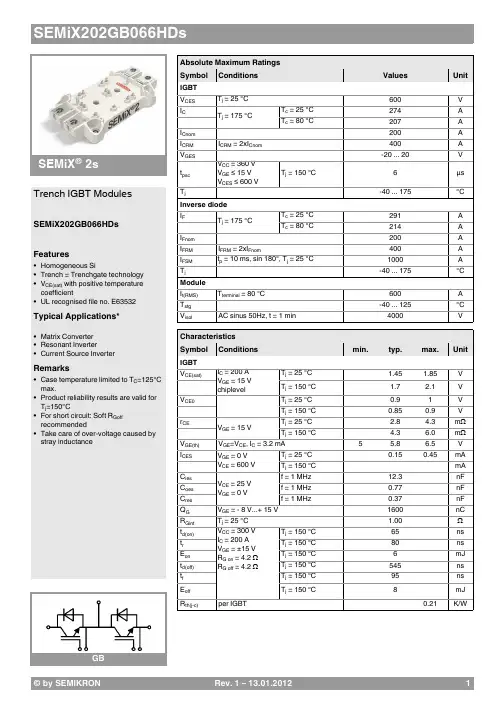
SEMiX ®2sTrench IGBT ModulesSEMiX202GB066HDsFeatures•Homogeneous Si•Trench = Trenchgate technology •V CE(sat) with positive temperature coefficient•UL recognised file no. E63532Typical Applications*•Matrix Converter •Resonant Inverter•Current Source InverterRemarks•Case temperature limited to T C =125°C max.•Product reliability results are valid for T j =150°C•For short circuit: Soft R Goff recommended•Take care of over-voltage caused by stray inductanceAbsolute Maximum Ratings SymbolConditions Values UnitIGBT V CES T j =25°C 600V I C T j =175°CT c =25°C 274A T c =80°C207A I Cnom 200A I CRMI CRM = 2xI Cnom 400A V GES -20 (20)V t psc V CC =360V V GE ≤ 15V V CES ≤ 600VT j =150°C6µs T j-40...175°C Inverse diode I F T j =175°CT c =25°C 291A T c =80°C 214A I Fnom200A I FRM I FRM = 2xI Fnom400A I FSM t p =10ms, sin 180°, T j =25°C1000A T j -40 (175)°C Module I t(RMS)T terminal =80°C600A T stg -40...125°C V isolAC sinus 50Hz, t =1min4000VCharacteristics SymbolConditions min.typ.max.UnitIGBT V CE(sat)I C =200A V GE =15V chiplevelT j =25°C 1.45 1.85V T j =150°C 1.7 2.1V V CE0T j =25°C 0.91V T j =150°C0.850.9V r CE V GE =15VT j =25°C 2.8 4.3m ΩT j =150°C4.3 6.0m ΩV GE(th)V GE =V CE , I C =3.2mA 55.86.5V I CES V GE =0V V CE =600V T j =25°C 0.150.45mA T j =150°C mA C ies V CE =25V V GE =0Vf =1MHz 12.3nF C oes f =1MHz 0.77nF C res f =1MHz0.37nF Q G V GE =- 8 V...+ 15 V 1600nC R Gint T j =25°C 1.00Ωt d(on)V CC =300V I C =200A V GE =±15V R G on =4.2ΩR G off =4.2ΩT j =150°C 65ns t r T j =150°C 80ns E on T j =150°C 6mJ t d(off)T j =150°C 545ns t f T j =150°C 95ns E off T j =150°C8mJ R th(j-c)per IGBT 0.21K/WCharacteristics SymbolConditionsmin.typ.max.UnitInverse diodeV F = V EC I F =200AV GE =0V chipT j =25°C 1.4 1.60V T j =150°C 1.4 1.6V V F0T j =25°C 0.91 1.1V T j =150°C0.750.850.95V r FT j =25°C 1.5 2.0 2.5m ΩT j =150°C2.32.83.3m ΩI RRM I F =200A di/dt off =3900A/µs V GE =-8VV CC =300VT j =150°C 205A Q rr T j=150°C28µC E rr T j =150°C 6.5mJR th(j-c)per diode0.27K/WModule L CE 18nH R CC'+EE'res., terminal-chip T C =25°C 0.7m ΩT C =125°C1m ΩR th(c-s)per module 0.045K/W M s to heat sink (M5)35Nm M tto terminals (M6)2.55Nm Nmw250gTemperatur Sensor R 100T c =100°C (R 25=5 k Ω)493 ± 5%ΩB 100/125R (T)=R 100exp[B 100/125(1/T-1/T 100)]; T[K];3550 ±2%K SEMiX ® 2sTrench IGBT ModulesSEMiX202GB066HDsFeatures•Homogeneous Si•Trench = Trenchgate technology •V CE(sat) with positive temperature coefficient•UL recognised file no. E63532Typical Applications*•Matrix Converter •Resonant Inverter•Current Source InverterRemarks•Case temperature limited to T C =125°C max.•Product reliability results are valid for T j =150°C•For short circuit: Soft R Goff recommended•Take care of over-voltage caused by stray inductanceFig. 1: Typ. output characteristic, inclusive R CC'+ EE'Fig. 2: Rated current vs. temperature I C = f (T C )Fig. 3: Typ. turn-on /-off energy = f (I C )Fig. 4: Typ. turn-on /-off energy = f (R G )Fig. 5: Typ. transfer characteristic Fig. 6: Typ. gate charge characteristicFig. 7: Typ. switching times vs. I C Fig. 8: Typ. switching times vs. gate resistor R GFig. 9: Typ. transient thermal impedance Fig. 10: Typ. CAL diode forward charact., incl. R CC'+EE'Fig. 11: Typ. CAL diode peak reverse recovery current Fig. 12: Typ. CAL diode recovery chargeThis is an electrostatic discharge sensitive device (ESDS), international standard IEC 60747-1, Chapter IX* The specifications of our components may not be considered as an assurance of component characteristics. Components have to be tested for the respective application. Adjustments may be necessary. The use of SEMIKRON products in life support appliances and systems is subject to prior specification and written approval by SEMIKRON. We therefore strongly recommend prior consultation of our staff.。
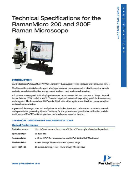
Microscope PlatformMicroscope Olympus®BX51 Reflected Illumination FrameLamp100 W Halogen Lamp, front mounted intensity control dial, user-adjustable photo presetswitch, LED voltage indicator lightsObjective lenses5x, 20x and 50x objective lenses provided as standard, 100x objective available as optional extra. Long working distance objective lens upgrade kit also available.Nosepiece Quadruple lens centering bright field nosepieceVideo camera USB video camera for sample alignmentStage Options Manual Stage Standard Motorized Stage Multi-well Sample StageRange of motion XY75 x 50 mm (3 x 2 in)75 x 50 mm (3 x 2 in)114 x 75 mm (4.5 x 3 in)Accuracy XY Verniers scale Stage movement accuracy of Stage movement accuracy of0.1 µ0.1 µDrive control XY Rackless, coarse and Joystick for XY sample Joystick for XY samplefine manual adjust-adjustment adjustmentment, tension adjust-ment mechanismAccuracy Z Fine stroke 100 µm Stage movement accuracy of Stage movement accuracy of per rotation, 1µm 0.1 µ0.1 µgradationDrive control Z Rack and pinion, Joystick for Z focus adjustment Joystick for Z focus adjustment coarse and fine manualadjustment, tensionadjustment mechanismAccessoriesGeneral Quartz microscope slides offer a low background and are ideal for mounting thin samplesMicro-sampling tool Consists of sampling tools specifically designed for manipulating and preparing microsamples. kit The kit includes pin vice, micro needle, stainless steel tweezers, dissecting forceps, razor knife and straight stainless-steel micro probe. This kit is provided as standard with the RamanMicro 200.Power sampling kit Stage mounted tablet autosampler accessory. Provided with 11, 15 and 22 mm diameter tablet holders. Compatible with PerkinElmer Tablet Autosampler molds for accommodating irregularshaped samples. Compatible with Leica®EM Trim supports for depth profiling. Standard andlarge stage versions available.Tablet sampling kit Stage mounted accessory accepts stainless steel sample cups. Provided with cup filler.Standard and large stage versions available.Hot stage Heating block and a temperature controller. The heating block contains an integral thermocouple;the temperature is digitally displayed in degrees Centigrade on the controller. The hot stagecan heat samples up to 230 ˚C in 1 ˚C increments. A target temperature may be selected andmaintained. The hot stage is held in the slide clip on the sample stage of manual and motorizedsample stages.Fiber Optic Probe (Optional Upgrade 200F only)General Switching from microscope to fiber optic probe is provided under software control. Data quoted here refers to the standard Raman probe. See Raman Fiber Optic Probes Technical SpecificationsProbe cable 5 m, armor clad with stainless steelProbe head length150 mmProbe head diameter12.7 mmWorking distance7.5 mmProbe spectral range230-3,500 cm-1 Raman shiftMax temperature80 ˚CUpgrade options Optional immersion sleeve for liquid immersion measurementsAdditional lengths of fiber optic cabling are available for use in environments where thesample is located at a distance from the spectrometer.A range of high temperature and high pressure probes is also available.Bench DetailsSize500 x 440 x 195 mm (spectrometer), 587 x 320 x 580 mm (microscope)Weight35 Kgs (spectrometer), 20 Kgs (microscope)Laser class RamanMicro 200 and 200F are Class 3b laser devices, and appropriate laser safety precautions should be observed.Power requirements110/240 VAC, 50/60 Hz (<50 W Typical)SoftwareSpectrum Software for spectral data acquisition and analysisGeneral A single software platform incorporates all of the functions required for Raman data acquisition and processing – instrument control, data manipulation and analysis, and flexible report utilities.A suite of optional software packages provide advanced capabilities or functions designed forspecific application areas.User interface Password-protected user login function. Access to methods and routines, menu, toolbar and toolbox functions can be controlled by a supervisor.Reports Quick print facility for graphs, spectra and results windows. User defined templates can be created to enable custom printed and electronic reports.Processing1st-4th derivative with a variable filter, smooth (Savitsky-Golay, moving average and triangular), difference, normalization, baseline correction, deconvolution, apex, interpolate, peak table,peak height and peak area.Materials testing Patented COMPARE™spectral comparison algorithm and Euclidean searching available.Spectral searching against commercially available or customer developed libraries.Quantitative analysis Single frequency, method development software. Spectrum includes Beer’s Law, PLS and PCR quantitative prediction.Validation Software allows performance verification to ASTM standards. Comprehensive IQ/OQdocumentation and services available.System diagnostics Key microscope and instrument components are checked on startup. Status of all RamanMicro components are displayed via PC control toolbox.SpectrumIMAGE Software for Chemical Imaging, provided with Motorized Stage based systems.Image presentation Chemical images can be generated from spectral analysis using average intensity, singlewavenumber, ChemiMap, Band Ratio, Quant+ result or COMPARE correlation, or by usingshow structure.Images can be viewed in false color, 3D projection or contour map.Show structure Single-click button operation to automate contrast enhancement in collected images byidentifying and revealing true spectral differences.Optional SoftwareQuant+Powerful chemometrics calibration building software.Spectrum Insight Quantitative high throughput screening and reaction monitoring. Insight works hand in hand with Quant+. Collected data is send to Quant+ which provides quantitative information, thisinformation is displayed in a simple to understand format, depending on the type of datacollected, Insight can represent the data in several ways:•High throughput mode: data shown in multiwell view using false color, grey scale orRed /Green (Pass/Fail).•Reaction monitoring: multiple concentrations to be viewed in graph format, screen isupdated in real time.•Spreadsheet: Data is presented in a spreadsheet format (compatible Microsoft®Excel®). PerkinElmer, Inc.940 Winter StreetWaltham, MA 02451 USAPhone: (800) 762-4000 or(+1) 203-925-4602For a complete listing of our global offices, visit /lasoffices©2007 PerkinElmer, Inc. All rights reserved. The PerkinElmer logo and design are registered trademarks of PerkinElmer, Inc. COMPARE, Quant+, RamanMicro, Spectrum and SpectrumIMAGE are trademarks and PerkinElmer is a registered trademark of PerkinElmer, Inc. or its subsidiaries, in the United States and other countries. Leica is a registered trademark of Leica Microsystems IR GMBH. Microsoft and Excel are registered trademarks of Microsoft Corporation. Olympus is a registered trademark of Olympus Optical Co., Ltd. All other trademarks not owned by PerkinElmer, Inc. or its subsidiaries that are depicted herein are the property of their respective owners. PerkinElmer reserves the right to change this document at any time without notice and disclaims liability for editorial, pictorial or typographical errors.007928A_02。

苏州普兆新能源设备有限公司地址:中国苏州平江区城北街道新塘工业区电话: +86 512 6878 6489传真: +86 512 6878 6489 苏州普兆新能源设备有限公司光伏专用开关技术手册目录公司简介 01应用领域 07CONTENT专业术语 03直流开关选择标准 05PROSOL-PVOBOX 43PROJO配电箱 45普兆直流开关单孔安装直流开关(16/25/32A) 13面板安装直流开关(16/25/32A) 15配电模式直流开关(16/25/32A) 17门锁安装直流开关(16/25/32A) 19外置直流开关(16/25/32A) 21单孔安装直流开关(40/55A) 23面板安装直流开关(40/55A) 25配电模式直流开关(40/55A) 27门锁安装直流开关(40/55A) 29外置直流开关(40/55A) 31普兆交流开关面板安装交流开关 33配电模式交流开关 25门锁安装交流开关 37外置交流开关 39产品参数总查询表 51营销网络 59ⅠⅡⅢⅣⅤⅥCOMPANY PROFILEAC .................................................................... 交流电DC ..................................................................... 直流电I e ............................................................ 额定工作电流I SC ..................................................................短路电流I th .......................................................................热电流MPPT ...................................................最大功率点跟踪PV .......................................................................光伏V OC ...................................................................断路电Impp .......................................................... MPPT电流AC-21............................电阻性负载切换,包括中度超载AC-22...............混合电阻和电感负载切换,包括中度效应DC-21......................... ..电阻性负载切换,包括中度超载DC-22...............混合电阻和电感负载切换,包括中度效应Disconnector ..................................................隔离开关Switch disconnector ...............负荷开关(负荷隔离开关)BS 7671...................................................电气装置要求EN 60364-7-712.........................《建筑物的电气设施》第7-712部分:特殊设施或场所的要求 – 太阳光电(PV)能源供应系统(IEC 60364-7-712,修订版)光伏电池: 基本的光伏设备,暴露在光照下(例如阳光)可以发电。
/tw 1EDS-2005-ELP 系列5埠入門級非網管型乙太網路交換器特色與優點•10/100BaseT(X)(RJ45連接器)•尺寸小巧並容易安裝•支援QoS 在高負荷流量中處理重要資料•IP40等級塑膠外殼認證簡介EDS-2005-ELP 系列工業級乙太網路交換器具有五個10/100M 網路埠及塑膠外殼,非常適合需要簡單工業級乙太網路連線的應用。
此外,為了針對不同產業的應用提供更多的彈性,EDS-2005-ELP 系列允許使用者透過外部面板DIP 開啟或停用服務品質功能(QoS )和廣播風暴防護(BSP )。
EDS-2005-ELP 系列具有12/24/48VDC 單電源輸入、DIN-Rail 鋁軌安裝,以及高等級EMI/EMC 防護能力。
除了小巧的尺寸之外,EDS-2005-ELP 系列也通過100%的高溫測試,確保在布署後能夠穩定運作。
EDS-2005-EL 系列具有-10至60°C 的標準操作溫度範圍。
規格Ethernet Interface10/100BaseT(X)Ports (RJ45connector)5Full/Half duplex modeAuto MDI/MDI-X connectionAuto negotiation speedStandardsIEEE 802.3for 10BaseTIEEE 802.1p for Class of ServiceIEEE 802.3u for 100BaseT(X)IEEE 802.3x for flow control Switch PropertiesProcessing TypeStore and Forward MAC Table Size8K Packet Buffer Size 4MbitsDIP Switch ConfigurationEthernet Interface Quality of Service (QoS),Broadcast Storm Protection (BSP)Power ParametersConnection1removable 3-contact terminal block(s)Input Current0.045A @24VDC Input Voltage12/24/48VDC Operating Voltage 9.6to 60VDCOverload Current Protection SupportedReverse Polarity Protection SupportedPhysical CharacteristicsDimensions19x81x65mm(0.74x3.19x2.56in) Installation DIN-rail mounting,Wall mounting(with optional kit) Weight56g(0.12lb)Housing PlasticEnvironmental LimitsAmbient Relative Humidity5to95%(non-condensing)Operating Temperature-10to60°C(14to140°F)Storage Temperature(package included)-40to85°C(-40to185°F)Standards and CertificationsSafety UL61010-2-201,EN62368-1(LVD)EMC EN55032/35EMI CISPR22,32,FCC Part15B Class AEMS IEC61000-4-2ESD:Contact:6kV;Air:8kVIEC61000-4-3RS:80MHz to1GHz:20V/mIEC61000-4-4EFT:Power:2kV;Signal:2kVIEC61000-4-5Surge:Power:2kV;Signal:2kVIEC61000-4-6CS:10VIEC61000-4-8PFMFShock IEC60068-2-27Vibration IEC60068-2-6Freefall IEC60068-2-32MTBFTime4,814,369hrsStandards Telcordia(Bellcore),GBWarrantyWarranty Period5yearsDetails See /tw/warrantyPackage ContentsDevice1x EDS-2005Series switchDocumentation1x quick installation guide1x warranty card2尺寸訂購資訊Model Name 10/100BaseT(X)Ports(RJ45connector)Housing Operating TemperatureEDS-2005-ELP5Plastic-10to60°C配件(選購)Power SuppliesDR-120-24120W/2.5A DIN-rail24VDC power supply with universal88to132VAC or176to264VAC input byswitch,or248to370VDC input,-10to60°C operating temperatureDR-452445W/2A DIN-rail24VDC power supply with universal85to264VAC or120to370VDC input,-10to50°Coperating temperatureDR-75-4875W/1.6A DIN-rail48VDC power supply with universal85to264VAC or120to370VDC input,-10to60°C operating temperatureMDR-40-24DIN-rail24VDC power supply with40W/1.7A,85to264VAC,or120to370VDC input,-20to70°Coperating temperatureMDR-60-24DIN-rail24VDC power supply with60W/2.5A,85to264VAC,or120to370VDC input,-20to70°Coperating temperatureWall-Mounting KitsWK-18Wall-mounting kit,1plate,18x120x8.5mmRack-Mounting KitsRK-4U19-inch rack-mounting kit©Moxa Inc.版權所有.2020年2月13日更新。
122EE-SX3081/-SX4081 Photomicrosensor (Transmissive)■DimensionsNote:All units are in millimeters unless otherwise indicated.■Features•Incorporates an IC chip with a built-in detector element and ampli-■Electrical and Optical Characteristics (Ta = 25°C)Internal CircuitDimensions Tolerance 3 mm max. ±0.33 < mm ≤ 6 ±0.3756 < mm ≤ 10 ±0.4510 < mm ≤ 18 ±0.5518 < mm ≤ 30±0.65Unless otherwise specified, the tolerances are as shown below.Terminal No. Name A Anode K Cathode V Power supply (Vcc)O Output (OUT)GGround (GND)KAV GOCross section AACross section BBOptical axisFour, C0.3Two, C1±0.3Five, 0.25±0.1(Five, 0.5±0.1)8.5±0.18.2±0.55±0.12.5±0.22.5+0.16.5±0.16.2±0.510±0.27.5±0.213.7+0.3(10.5)(2.5)ItemSymbol ValueConditionEmitterForward voltage V F1.2 V typ., 1.5 V max.I F = 20 mA Reverse current I R 0.01 μA typ., 10 μA max.V R = 4 V Peak emission wave-lengthλP 940 nm typ.I F = 20 mADetectorLow-level output volt-ageV OL 0.12 V typ., 0.4 V max.V CC = 4.5 to 16 V, I OL = 16 mA, I F = 0 mA (EE-SX3081), I F = 8 mA (EE-SX4081)High-level output volt-ageV OH 15 V min.V CC = 16 V, R L = 1 k Ω, I F = 8 mA (EE-SX3081), I F = 0 mA (EE-SX4081)Current consumptionI CC3.2 mA typ., 10 mA max.V CC = 16 V Peak spectral sensitivi-ty wavelengthλP 870 nm typ.V CC = 4.5 to 16 V LED current when output is OFF I FT8 mA max.V CC = 4.5 to 16 VLED current when output is ON HysteresisΔH 15% typ.V CC = 4.5 to 16 V (see note 1)Response frequency f 3 kHz min.V CC = 4.5 to 16 V, I F = 20 mA, I OL = 16 mA (see note 2)Response delay time t PLH (t PHL ) 3 μs typ.V CC = 4.5 to 16 V, I F = 20 mA, I OL = 16 mA (see note 3)Response delay timet PHL (t PLH )20 μs typ.V CC = 4.5 to 16 V, I F = 20 mA, I OL = 16 mA (see note 3)Be sure to read Precautions on page 25.EE-SX3081/-SX4081 Photomicrosensor (Transmissive) 123■Engineering DataNote:The values in the parentheses apply to the EE-SX4081.2.1 mm0.5 mm0.5 mmDiskInput OutputInput OutputEE-SX3081EE-SX4081Note: 1. H ysteresis denotes the difference in forward LEDcurrent value, expressed in percentage, calculated from the respective forward LED currents when the photo IC in turned from ON to OFF and when the photo IC in turned from OFF to ON.2. The value of the response frequency is measured by rotating the disk as shown below.3. The following illustrations show the definition of response delay time. The value in the parentheses applies to the EE-SX4081.Forward Current vs. Collector Dissipation Temperature RatingForward Current vs. Forward Voltage Characteristics (Typical)LED Current vs. Supply Voltage (Typical)Low-level Output Voltage vs. Output Current (Typical)Current Consumption vs. Supply Voltage (Typical)Response Delay Time vs. Forward Current (Typical)Repeat Sensing Position Characteristics (Typical)O u t p u t t r a n s i s t o rDistance d (mm)Center of optical axisSupply voltage V CC (V)L o w l e v e l o u t p u t v o l t a g e V O L (V )C u r r e n t c o n s u m p t i o n I c c (m A )Supply voltage V CC (V)Forward current I F (mA)I FT OFF (I FT ON)I FT ON (I FT OFF)V CC = 5 VI F = 0 mA (15 mA)I OL = 16 mAI OL = 5 mAT a = 25°CI F = 0 mA (15 mA)V CC = 5 V R L = 330 Ω Ta = 25°CV OUT(EE-SX3@@)V OUT(EE-SX4@@)T a = 25°C I F = 15 mA V CC = 5 V R L = 330 Ωn = repeat 20 timesd 1 = 0.01 mmAmbient temperature T a (°C)O u t p u t a l l o w a b l e d i s s i p a t i o n P C (m W )Forward voltage V F (V)F o r w a r d c u r r e n t I F (m A )F o r w a r d c u r r e n t I F (m A )L E D c u r r e n t I F T (m A )T a = 25°C R L = 1 k ΩR e s p o n s e d e l a y t i m e t P H L , t P L H (μs )I F = 0 mA (15 mA)V CC = 5 VT a = 25°C L E D c u r r e n t I F T (m A )I FT OFF (I FT ON)I FT ON (I FT OFF)Ambient temperature T a (°C)V CC = 5 V R L = 330 ΩTa = −30°C Ta = 25°C Ta = 70°CL o w l e v e l o u t p u t v o l t a g e V O L (V )Output current I C (mA)Ambient temperature Ta (°C)Low-level Output Voltage vs. Am-bient Temperature Characteristics (Typical)LED Current vs. Ambient Temper-ature Characteristics (Typical)。
3W/5W ,AC-DC模块电源CB RoHS产品特点●全球通用电压:85-264VAC/100-370VDC ●工作温度范围:-40℃to +70℃●4000VAC 高隔离电压●稳压输出、低纹波噪声●输出短路、过流、过压保护●高效率、高可靠性●全塑料外壳,符合UL94V-0●EMI 性能满足CISPR32/EN55032CLASS B●符合IEC62368、UL62368、EN62368认证标准(认证中)LDE03/05-20Bxx 系列------是金升阳为客户提供的小体积开关模块电源。
该系列电源具有全球输入电压范围、交直流两用、低功耗、高效率、安全隔离等优点。
产品安全可靠。
该系列产品应用在电磁兼容比较恶劣的环境下时必须参考应用电路。
选型表认证型号输出功率标称输出电压及电流(Vo/Io)效率(230VAC/%,Typ.)最大容性负载(uF )UL/CE/CB (认证中)LDE03-20B03 2.3W3.3V/700mA 666000LDE03-20B053W5V/600mA 746000LDE03-20B099V/330mA 751500LDE03-20B1212V/250mA 771500LDE03-20B1515V/200mA 771000LDE03-20B2424V/125mA 78330LDE05-20B03 3.3W 3.3V/1000mA 685000LDE05-20B055W 5V/1000mA 755000LDE05-20B099V/560mA 771200LDE05-20B1212V/420mA 791200LDE05-20B1515V/330mA 791000LDE05-20B2424V/210mA81330输入特性项目工作条件Min.Typ.Max.单位输入电压范围交流输入85--264VAC 直流输入100--370VDC 输入频率47--63Hz输入电流LDE03115V AC ----80mA230V AC ----45LDE05115V AC ----130230V AC----70冲击电流115V AC --10--A230V AC--20--漏电流0.1mA RMS typ.230V AC/50Hz外接保险管推荐值1A/250V ,慢断,必接热插拔不支持项目工作条件Min.Typ.Max.单位输出电压精度 3.3V 输出--±3--%其它--±2--线性调节率满载--±0.5--负载调节率0%-100%负载--±1--输出纹波噪声*20MHz 带宽(峰-峰值)--50100mV 温漂系数--±0.02--%/℃短路保护打嗝式,可长期短路,自恢复过流保护LDE03≥150%Io 自恢复LDE05≥120%Io 自恢复过压保护3.3/5VDC 输出≤7.5VDC 9VDC 输出≤15VDC 12/15VDC 输出≤20VDC 24VDC 输出≤30VDC最小负载0----%掉电保持时间LDE03115V AC 输入--10--ms 230V AC 输入--60--LDE05115V AC 输入--5--230V AC 输入--50--注:*纹波和噪声的测试方法采用平行线测试法,具体操作方法参见《AC-DC 模块电源应用指南》。
目錄 :PEX-1X卡介紹 (02)功能介紹 (02)產品內容 (03)光碟內容 (04)瞭解PEX-1X卡 (04)硬體圖片 (04)系統功能 (05)硬體設定 (06)LED指示燈說明 (07)系統安裝 (08)硬體安裝 (08)使用模式 (09)軟體安裝 (11)目錄及檔案 (14)軟體使用及操作 (16)視窗功能介紹 (16)設定功能單元 (17)主操作視窗單元 (18)量產模式操作流程 (24)工程模式操作流程 (27)電流校正操作 (28)系統設定 (29)軟體解除安裝 (32)注意事項與故障排除 (33)附註說明 (35)連絡方式 (36)PEX-1X PCIe Hot Swap Extender是一PCI Express x1單片延伸保護卡,適用於第三代PCIe 匯流排(PCI Express Bus)相容的PC。
提供隔離主機板的PCIe與待測卡 (Device Under Test 以下簡稱DUT)之間所有電源及訊號的功能,方便於進行熱插拔換卡驗證與測試。
隔離功能可利用延伸保護卡本身內建的電源開關手動控制或透過軟體遠程控制。
熱插拔換卡功能可免除使用者於測試驗證時,需關閉PC 電源及作業系統或重覆開關機的動作,可讓工程人員或測試人員於PC保持開機狀態下,運用本產品及所提供的程式,就可作相關的PCIe待測裝置(Hot Swap)換卡測試驗證的動作,免去換卡測試需要重新開關PC所浪費的時間,有效縮短測試時間,增加產能及快速測試的效率。
搭配本產品的自動開關功能及插入自動啟動測試功能,可簡化測試動作,進一步增加測試速率並減少人為操作失誤,達到自動化測試的要求。
保護功能提供短路及過電流(過載)保護。
在使用者欲測試不明狀態或故障的PCIe 介面卡時,以優異準確之各組直流電源( +3.3V,+12V, +3.3VAUX)監控設計, 確保PCIe 待測裝置正常工作。
一旦出現短路或超出正常電壓、電流時,PEX-1X 會立即切斷插槽上的電源,以保護PC主機及待測裝置不被燒毀。
PMC232/PMS232系列带12位ADC、采用FPPA TM技术双核心8位单片机数据手册第0.03版2017年3月27日Copyright 2017 by PADAUK Technology Co., Ltd., all rights reserved10F-2, No. 1, Sec. 2, Dong-Da Road, Hsin-Chu 300, Taiwan, R.O.C.重要声明应广科技保留权利在任何时候变更或终止产品,建议客户在使用或下单前与应广科技或代理商联系以取得最新、最正确的产品信息。
应广科技不担保本产品适用于保障生命安全或紧急安全的应用,应广科技不为此类应用产品承担任何责任。
关键应用产品包括,但不仅限于,可能涉及的潜在风险的死亡,人身伤害,火灾或严重财产损失。
应广科技不承担任何责任来自于因客户的产品设计所造成的任何损失。
在应广科技所保障的规格范围内,客户应设计和验证他们的产品。
为了尽量减少风险,客户设计产品时,应保留适当的产品工作范围安全保障。
提供本文档的中文简体版是为了便于了解,请勿忽视文中英文的部份,因为其中提供有关产品性能以及产品使用的有用信息,应广科技暨代理商对于文中可能存在的差错不承担任何责任,建议参考本文件英文版。
目录1. 单片机特点 (8)1.1. 系列特点 (8)1.2. 高性能RISC CPU架构 (8)1.3. 系统功能 (8)1.4. 封装信息 (9)2. 系统概述和方框图 (10)3. PMC232系列引脚功能描述 (11)4. PMS232系列引脚功能描述 (12)5. 器件电气特性 (15)5.1. 直流/交流特性 (15)5.2. 最大范围 (17)5.3. ILRC频率与VDD、温度关系的曲线图 (18)5.4. IHRC频率与VDD、温度关系的曲线图 (19)5.5. 工作电流量测值@系统时钟=ILRC÷N (20)5.6. 工作电流量测值@系统时钟=IHRC÷N (20)5.7. 工作电流量测值@系统时钟=4MH Z晶振EOSC÷N (21)5.8. 工作电流量测值@系统时钟=32K H Z晶振EOSC÷N (21)5.9. IO引脚输出驱动电流(I OH)和灌电流(I OL)曲线图 (22)5.10. 测量的IO输入阈值电压(V IH/V IL) (22)5.11. IO引脚拉高阻抗曲线图 (22)5.12. 输出(VDD/2)偏置电压与VDD关系的曲线图 (23)5.13. 开机时序图 (23)6. 功能概述 (24)6.1. 处理单元 (24)6.1.1程序计数器 (25)6.1.2 堆栈指针 (25)6.1.3 一个处理单元工作模式 (26)6.2. OTP程序存储器 (27)6.2.1 程序存储器分配 (27)6.2.2 两个处理单元工作模式下程序存储器分配例子 (27)6.2.3 一个处理单元工作模式下程序存储器分配例子 (28)6.3 程序结构 (29)6.3.1 两个处理单元工作模式下程序结构 (29)6.3.2 一个处理单元工作模式下程序结构 (29)6.4 启动程序 (30)6.5 数据存储器 (31)6.6 算术和逻辑单元 (31)6.7 振荡器和时钟 (32)6.7.1 内部高频振荡器(IHRC)和低频振荡器(ILRC) (32)6.7.2 单片机校准 (32)6.7.3 IHRC频率校准和系统时钟 (32)6.7.4 晶体振荡器 (34)6.7.5 系统时钟和LVR水平 (35)6.7.6 系统时钟切换 (36)6.8 16位定时器(T IMER16) (37)6.9 8位PWM定时器(T IMER2) (39)6.9.1 使用Timer2产生定期波形 (40)6.9.2 使用Timer2产生8位PWM波形 (41)6.9.3 使用Timer2产生6位PWM波形 (43)6.10 看门狗定时器 (44)6.11 中断 (45)6.12 掉电模式 (47)6.12.1 省电模式(stopexe) (47)6.12.2 掉电模式(stopsys) (48)6.12.3 唤醒 (49)6.13 IO端口 (50)6.14 复位和LVR (51)6.14.1 复位 (51)6.14.2 LVR (51)6.15 VDD/2偏置电压 (51)6.16 数字转换(ADC)模块 (52)6.16.1 AD转换的输入要求 (53)6.16.2 ADC分辨率选择 (54)6.16.3 ADC 时钟选择 (54)6.16.4 AD转换 (54)6.16.5 模拟引脚的配置 (54)6.16.6 使用ADC (54)7. IO寄存器 (55)7.1 算术逻辑状态寄存器(FLAG),IO地址=0X00 (55)7.2 FPP单元允许寄存器(FPPEN),IO地址=0X01 (55)7.3 堆栈指针寄存器(SP),IO地址=0X02 (55)7.4 时钟控制寄存器(CLKMD),IO地址=0X03 (56)7.5 中断允许寄存器(INTEN),IO地址=0X04 (56)7.6 中断请求寄存器(INTRQ),IO地址=0X05 (56)7.7 T IMER16控制寄存器(T16M),IO地址=0X06 (57)7.8 通用数据输入/输出寄存器(GDIO),IO地址=0X07 (57)7.9 外部晶体振荡器控制寄存器(EOSCR),IO地址=0X0A (57)7.10 内部高频RC振荡器控制寄存器(IHRCR,只写),IO地址=0X0B (58)7.11 中断边沿选择寄存器(INTEGS,只写),IO地址=0X0C (58)7.12 端口A数字输入禁止寄存器(PADIER,只写),IO地址=0X0D (58)7.13 端口B数字输入禁止寄存器(PBDIER,只写),IO地址=0X0E (59)7.14 端口A数据寄存器(PA),IO地址=0X10 (59)7.15 端口A控制寄存器(PAC),IO地址=0X11 (59)7.16 端口A上拉控制寄存器(PAPH),IO地址=0X12 (59)7.17端口B数据寄存器(PB),IO地址=0X14 (59)7.18端口B控制寄存器(PBC),IO地址=0X15 (59)7.19 端口B上拉控制寄存器(PBPH),IO地址=0X16 (60)7.20 端口C数据寄存器(PC),IO地址=0X17 (60)7.21 端口C控制寄存器(PCC),IO地址=0X18 (60)7.22 端口C上拉控制寄存器(PCPH),IO地址=0X19 (60)7.23 ADC控制寄存器(ADCC),IO地址=0X20 (60)7.24 ADC模式控制寄存器(ADCM,只写),IO地址=0X21 (61)7.25 ADC数据高位寄存器(ADCRH,只读),IO地址=0X22 (61)7.26 ADC数据低位寄存器(ADCRL,只读),IO地址=0X23 (61)7.27 杂项寄存器(MISC),IO地址=0X3B (62)7.28 T IMER2控制寄存器(TM2C),IO地址=0X3C (63)7.29 T IMER2计数寄存器(TM2CT),IO地址=0X3D (63)7.30 T IMER2分频器寄存器(TM2S),IO地址=0X37 (63)7.31 T IMER2上限寄存器(TM2B),IO地址=0X09 (64)8. 指令 (65)8.1 数据传输类指令 (65)8.2 算术运算类指令 (69)8.3 移位运算类指令 (71)8.4 逻辑运算类指令 (72)8.5 位运算类指令 (74)8.6 条件运算类指令 (75)8.7 系统控制类指令 (77)8.8 指令执行周期综述 (79)8.9 指令影响标志的综述 (80)9. 特别注意事项 (81)9.1 警告 (81)9.2 使用IC时 (81)9.2.1 IO使用与设定 (81)9.2.2 中断 (82)9.2.3 切换系统时钟 (82)9.2.4 掉电模式、唤醒以及看门狗 (83)9.2.5 TIMER溢出时间 (84)9.2.6 ADC使用注意事项 (84)9.2.7 LVR (84)9.2.8 IHRC (84)9.2.9 单/双核模式下指令周期差异 (85)9.3 使用ICE时 (85)9.3.1 PMC232/PMS232系列于仿真器PDK3S-I-001/002/003上仿真时 (85)9.3.2 使用PDK3S-I-001/002/003仿真PMC232/PMS232系列功能時注意事項 (86)修订历史:修订日期描述0.01 2015/8/1 初版。
2.5V or3.3V,10- 220 MHz, Low Jitter, 5 OutputZero Delay BufferCY23EP05Features•10 MHz to 220 MHz maximum operating range •Zero input-output propagation delay, adjustable by loading on CLKOUT pin •Multiple low-skew outputs—30 ps typical output-output skew —One input drives five outputs •22 ps typical cycle-to-cycle jitter •13 ps typical period jitter•Standard and High drive strength options •Available in space-saving 150-mil SOIC package •3.3V or 2.5V operation•Industrial temperature availableFunctional DescriptionThe CY23EP05 is a 2.5V or 3.3V zero delay buffer designed to distribute low-jitter high-speed clocks and is available in a 8-pin SOIC package. It accepts one reference input, and drives out five low-skew clocks. The -1H version operates up to 220 (200) MHz frequencies at 3.3V (2.5V), and has a higher drive strength than the -1 devices. All parts have on-chip PLLs which lock to an input clock on the REF pin. The PLL feedback is on-chip and is obtained from the CLKOUT pad.The CY23EP05 PLL enters a power-down mode when there are no rising edges on the REF input (<~2 MHz). In this state,the outputs are three-stated and the PLL is turned off, resulting in less than 25 µA of current draw.The CY23EP05 is available in different configurations, as shown in the Ordering Information table. The CY23EP05-1 is the base part. The CY23EP05-1H is the high-drive version of the -1, and its rise and fall times are much faster than the -1. These parts are not intended for 5V input-tolerant applicationsBlock DiagramPin Configuration12345876REF CLK2CLK1GNDV DD CLKOUT CLK4CLK3Top ViewPLLREFCLK1CLK2CLK3CLK4CLKOUTZero Delay and Skew ControlAll outputs should be uniformly loaded to achieve Zero Delay between the input and output. Since the CLKOUT pin is the internal feedback to the PLL, its relative loading can adjust the input-output delay.The output driving the CLKOUT pin will be driving a total load of 5 pF plus any additional load externally connected to thispin. For applications requiring zero input-output delay, the total load on each output pin (including CLKOUT) must be the same. If input-output delay adjustments are required, the CLKOUT load may be changed to vary the delay between the REF input and remaining outputs.For zero output-output skew, be sure to load all outputs equally. For further information refer to the application note titled “CY2305 and CY2309 as PCI and SDRAM Buffers”.Notes:1.Weak pull-down.2.Weak pull-down on all outputs.3.This output is driven and has an internal feedback for the PLL. The load on this output can be adjusted to change the skew between the reference and output.Pin DescriptionPin SignalDescription1REF [1]Input reference frequency 2CLK2[2]Buffered clock output 3CLK1[2]Buffered clock output 4GND Ground5CLK3[2]Buffered clock output 6V DD 3.3V or 2.5V supply 7CLK4[2]Buffered clock output8CLKOUT [2,3]Buffered clock output, internal feedback on this pinAbsolute Maximum ConditionsSupply Voltage to Ground Potential.................–0.5V to 4.6V DC Input Voltage......................................V SS – 0.5V to 4.6V Storage Temperature....................................–65°C to 150°C Junction Temperature..................................................150°C Static Discharge Voltage(per MIL-STD-883, Method 3015..............................> 2000VOperating ConditionsParameter Description Min.Max.Unit V DD3.3 3.3V Supply Voltage 3.0 3.6VV DD2.5 2.5V Supply Voltage 2.3 2.7VT A Operating Temperature (Ambient Temperature)—Commercial070°C Operating Temperature (Ambient Temperature)—Industrial–4085°CC L[4]Load Capacitance, <100 MHz, 3.3V–30pFLoad Capacitance, <100 MHz, 2.5V with High drive–30pFLoad Capacitance, <133.3 MHz, 3.3V–22pFLoad Capacitance, <133.3 MHz, 2.5V with High drive–22pFLoad Capacitance, <133.3 MHz, 2.5V with Standard drive–15pFLoad Capacitance, >133.3 MHz, 3.3V–15pFLoad Capacitance, >133.3 MHz, 2.5V with High drive–15pFC IN Input Capacitance[5]–5pF BW Closed-loop bandwidth (typical), 3.3V1–1.5MHz Closed-loop bandwidth (typical), 2.5V0.8MHz R OUT Output Impedance (typical), 3.3V High drive29ΩOutput Impedance (typical), 3.3V Standard drive41ΩOutput Impedance (typical), 2.5V High drive37ΩOutput Impedance (typical), 2.5V Standard drive41Ωt PU Power-up time for all VDD’s to reach minimum specified voltage(power ramps must be monotonic)0.0150ms Theta Ja[6]Dissipation, Junction to Ambient, 8-pin SOIC131°C/W Theta Jc[6]Dissipation, Junction to Case, 8-pin SOIC81°C/W 3.3V DC Electrical SpecificationsParameter Description Test Conditions Min.Max.Unit V DD Supply Voltage 3.0 3.6V V IL Input LOW Voltage–0.8V V IH Input HIGH Voltage 2.0V DD + 0.3V I IL Input Leakage Current0 < V IN < V IL–±10µA I IH Input HIGH Current V IN = V DD–100µAV OL Output LOW Voltage I OL = 8 mA (standard drive)I OL = 12 mA (High drive)––0.40.4VVV OH Output HIGH Voltage I OH = –8 mA (standard drive)I OH = –12 mA (High drive)2.42.4––VVI DD (PD mode)Power Down Supply Current REF = 0 MHz (Commercial)–12µAREF = 0 MHz (Industrial)–25µA I DD Supply Current Unloaded outputs, 66-MHz REF –30mA Notes:4.Applies to Test Circuit #1.5.Applies to both REF Clock and internal feedback path on CLKOUT.6.Theta Ja, EIA JEDEC 51 test board conditions, 2S2P; Theta Jc Mil-Spec 883E Method 1012.1.2.5V DC Electrical SpecificationsParameter Description Test Conditions Min.Max.Unit V DD Supply Voltage 2.3 2.7V V IL Input LOW Voltage–0.7V V IH Input HIGH Voltage 1.7V DD + 0.3V I IL Input Leakage Current0<V IN < V DD–10µA I IH Input HIGH Current V IN = V DD–100µAV OL Output LOW Voltage I OL = 8 mA (Standard drive)I OL = 12 mA (High drive)––0.50.5VVV OH Output HIGH Voltage I OH = –8 mA (Standard drive)I OH = –12 mA (High drive)V DD – 0.6V DD – 0.6––VVI DD (PD mode)Power Down Supply Current REF = 0 MHz (Commercial)–12µAREF = 0 MHz (Industrial)–25µAI DD Supply Current Unloaded outputs, 66-MHz REF –45mA3.3V and 2.5V AC Electrical SpecificationsParameter Description Test Conditions Min.Typ.Max.Unit1/t1Maximum Frequency[7](Input/Output)3.3V High drive10–220MHz 3.3V Standard drive10–167MHz 2.5V High drive10–200MHz 2.5V Standard drive10–133MHzT IDC Input Duty Cycle<133.3 MHz25–75%>133.3 MHz40–60% t2 ÷ t1Output Duty Cycle[8]<133.3 MHz47–53%>133.3 MHz45–55% t3,t4Rise, Fall Time (3.3V)[8]Std drive, CL = 30 pF, <100 MHz–– 1.6nsStd drive, CL = 22 pF, <133.3 MHz–– 1.6nsStd drive, CL = 15 pF, <167 MHz––0.6nsHigh drive, CL = 30 pF, <100 MHz–– 1.2nsHigh drive, CL = 22 pF, <133.3 MHz–– 1.2nsHigh drive, CL = 15 pF, >133.3 MHz––0.5ns t3, t4Rise, Fall Time (2.5V)[8]Std drive, CL = 15 pF, <133.33 MHz–– 1.5nsHigh drive, CL = 30 pF, <100 MHz–– 2.1nsHigh drive, CL = 22 pF, <133.3 MHz–– 1.3nsHigh drive, CL = 15 pF, >133.3 MHz–– 1.2ns t5Output to Output Skew [8]All outputs equally loaded–30100pst6Delay, REF Rising Edge toCLKOUT Rising Edge[8]PLL enabled @ 3.3V–100–100ps PLL enabled @2.5V–200–200pst7Part to Part Skew[8]Measured at V DD/2.Any output to any output, 3.3V supply––±150psMeasured at V DD/2.Any output to any output, 2.5V supply––±300psNotes:7.For the given maximum loading conditions. See C L in Operating Conditions Table.8.Parameter is guaranteed by design and characterization. Not 100% tested in production.t LOCK PLL Lock Time [8]Stable power supply, valid clocks presented on REF and CLKOUT pins–– 1.0ms T JCC [8,9]Cycle-to-cycle Jitter, Peak 3.3V supply, >66 MHz, <15 pF–2255ps 3.3V supply, >66 MHz, <30 pF, standard drive –45125ps 3.3V supply, >66 MHz, <30 pF, high drive –45100ps 2.5V supply, >66 MHz, <15 pF, standard drive –40100ps 2.5V supply, >66 MHz, <15 pF, high drive –3580ps 2.5V supply, >66 MHz, <30 pF, high drive–52125ps T PER [8,9]Period Jitter, Peak3.3V supply, 66–100 MHz, <15 pF –1860ps 3.3V supply, >100 MHz, <15 pF–1335ps 3.3V supply, >66 MHz, <30 pF, standard drive –2875ps 3.3V supply, >66 MHz, <30 pF, high drive –2670ps 2.5V supply, >66 MHz, <15 pF, standard drive –2560ps 2.5V supply, 66–100 MHz, <15 pF, high drive –2260ps 2.5V supply, >100 MHz, <15 pF, high drive–1945ps3.3V and 2.5V AC Electrical Specifications (continued)Parameter DescriptionTest ConditionsMin.Typ.Max.Unit Switching WaveformsNote:9.Typical jitter is measured at 3.3V or 2.5V, 29°C, with all outputs driven into the maximum specified load. Further information regarding jitter specifications may be found in the application notes, “Understanding Data Sheet Jitter Specifications for Cypress Products.”Duty Cycle Timingt 1t 2V DD /2V DD /2V DD /2All Outputs Rise/Fall TimeOUTPUT t 33.3V(2.5V)0V0.8V(0.6V)2.0V(1.8V)2.0V(1.8V)0.8V(0.6V)t 4Output-Output Skewt 5OUTPUTOUTPUTV DD /2V DD /2Switching Waveforms (continued)Input-Output Propagation DelayV DD /2t 6INPUTCLKOUTV DD /2V DD /2V DD /2t 7Any output, Part 1 or 2Any output, Part 1 or 2Part-Part SkewTest Circuits0.1µFV DD0.1µFV DDCLKC LOADOUTPUTSGNDGNDTest Circuit # 1Supplemental Parametric InformationFigure 1. 2.5V Typical Room Temperature Graph for REF Input to CLKn Delay versus Loading Difference between CLKOUT and CLKn. Data is shown for 66 MHz. Delay is a weak function of frequency.Figure 2. 3.3V Typical Room Temperature Graph for REF Input to CLKn Delay versus Loading Difference between CLKOUT and CLKn. Data is shown for 66 MHz. Delay is a weak function of frequency.Figure 3. 2.7V Measured Supply Current versus Frequency, Drive Strength, Loading, and Temperature. Note that the 30-pF data above 100 MHz is beyond the data sheet specification of 22 pF.Figure 4. 3.6V Measured Supply Current versus Frequency, Drive Strength, Loading, and Temperature. Note that the 30-pF high-drive data above 100 MHz is beyond the data sheet specification of 22 pF.Figure 5. Typical 3.3V Measured Cycle-to-cycle Jitter at 29°C, versus Frequency, Drive Strength, and LoadingFigure 6. Typical 2.5V Measured Cycle-to-cycle Jitter at 29°C, versus Frequency, Drive Strength, and LoadingFigure 7. Typical 3.3V Measured Period Jitter at 29°C, versus Frequency, Drive Strength, and LoadingFigure 8. Typical 2.5V Measured Period Jitter at 29°C, versus Frequency, Drive Strength, and LoadingFigure 9. 100 MHz (top) and 156.25 MHz (bottom) Typical Phase-noise Data versus V DD and Drive Strength[9]Ordering InformationOrdering Code Package Type Operating Range Lead-freeCY23EP05SXC-18-pin 150-mil SOIC CommercialCY23EP05SXC-1T8-pin 150-mil SOIC – Tape and Reel CommercialCY23EP05SXI-18-pin 150-mil SOIC IndustrialCY23EP05SXI-1T8-pin 150-mil SOIC – Tape and Reel IndustrialCY23EP05SXC-1H8-pin 150-mil SOIC CommercialCY23EP05SXC-1HT8-pin 150-mil SOIC – Tape and Reel CommercialCY23EP05SXI-1H8-pin 150-mil SOIC IndustrialCY23EP05SXI-1HT8-pin 150-mil SOIC – Tape and Reel IndustrialPackage Drawing and DimensionsAll product and company names mentioned in this document may be the trademarks of their respective holders.Document #: 38-07759 Rev. *B Page 11 of 12© Cypress Semiconductor Corporation, 2005. The information contained herein is subject to change without notice. Cypress Semiconductor Corporation assumes no responsibility for the use of any circuitry other than circuitry embodied in a Cypress product. Nor does it convey or imply any license under patent or other rights. Cypress products are not warranted nor intended to be used for medical, life support, life saving, critical control or safety applications, unless pursuant to an express written agreement with Cypress. Furthermore, Cypress does not authorize its products for use as critical components in life-support systems where a malfunction or failure may reasonably be expected to result in significant injury to the user. The inclusion of Cypress products in life-support systems application implies that the manufacturer assumes all risk of such use and in doing so indemnifies Cypress against all charges.Document History PageDocument Title: CY23EP05 2.5V or 3.3V, 10-220-MHz, Low Jitter, 5 Output Zero Delay Buffer Document Number: 38-07759REV.ECN NO.Issue Date Orig. ofChange Description of Change**349620See ECN RGL New data sheet*A401073See ECN RGL Updated Delay vs. Load graph with standard drive dataAdded Phase-noise graph*B413826See ECN RGL Minor Change: typo - changed from CY23EP05SXC-T to CY23EP05SXC-1TDocument #: 38-07759 Rev. *B Page 12 of 12。