
FEATURES
Computes
True rms value
Average rectified value
Absolute value
Provides 200 mV full-scale input range (larger inputs with input attenuator)
High input impedance: 1012 Ω
Low input bias current: 25 pA maximum
High accuracy: ±0.3 mV ± 0.3% of reading
RMS conversion with signal crest factors up to 5
Wide power supply range: +2.8 V, ?3.2 V to
±16.5V
Low power: 200 mA maximum supply current
Buffered voltage output
No external trims needed for specified accuracy
AD737—an unbuffered voltage output version with
chip power-down also available
GENERAL DESCRIPTION
The AD736 is a low power, precision, monolithic true rms-to-dc converter. It is laser trimmed to provide a maximum error of ±0.3 mV ± 0.3% of reading with sine wave inputs. Furthermore, it maintains high accuracy while measuring a wide range of input waveforms, including variable duty-cycle pulses and triac (phase)-controlled sine waves. The low cost and small size of this converter make it suitable for upgrading the performance of non-rms precision rectifiers in many applications. Compared to these circuits, the AD736 offers higher accuracy at an equal or lower cost.
The AD736 can compute the rms value of both ac and dc input voltages. It can also be operated as an ac-coupled device by adding one external capacitor. In this mode, the AD736 can resolve input signal levels of 100 μVrms or less, despite variations in temperature or supply voltage. High accuracy is also maintained for input waveforms with crest factors of 1 to 3. In addition, crest factors as high as 5 can be measured (introducing only 2.5% additional error) at the 200 mV full-scale input level.
The AD736 has its own output buffer amplifier, thereby pro-viding a great deal of design flexibility. Requiring only 200 μA of power supply current, the AD736 is optimized for use in portable multimeters and other battery-powered applications.
The AD736 allows the choice of two signal input terminals: a high impedance FET input (1012 Ω) that directly interfaces with High-Z input attenuators and a low impedance input (8 kΩ) that allows the measurement of 300 mV input levels while
operating from the minimum power supply voltage of +2.8 V, ?3.2 V. The tw o inputs can be used either single ended or differentially.
The AD736 has a 1% reading error bandwidth that exceeds 10 kHz for the input amplitudes from 20 mV rms to 200 mV rms while consuming only 1 mW.
The AD736 is available in four performance grades. The AD736J and AD736K grades are rated over the 0°C to +70°C and ?20°C to +85°C commercial temperature ranges.
The AD736A and AD736B grades are rated over the ?40°C to +85°C industrial temperature range. The AD736 is available in three low cost, 8-lead packages: PDIP, SOIC, and CERDIP.
PRODUCT HIGHLIGHTS
1. The AD736 is capable of computing the average rectified value, absolute value, or true rms value of various input signals.
2. Only one external component, an averaging capacitor, is required for the AD736 to perform true rms measurement.
3. The low power consumption of 1 mW makes the AD736 suitable for many battery-powered applications.
4. A high input impedance of 1012 Ω eliminates the need for an external buffer when interfacing with input attenuators.
5. A low impedance input is available for those applications that require an input signal up to 300 mV rms operating from low power supply voltages. SPECIFICATIONS
At 25°C ± 5 V supplies, ac-coupled with 1 kHz sine wave input applied, unless otherwise noted. Specifications in bold are tested on all production units at final electrical test. Results from those tests are used to calculate outgoing quality levels. Stresses above those listed under Absolute Maximum Ratings may cause permanent damage to the device. This is a stress rating only; functional operation of the device at these or any other conditions above those indicated in the operational section of this specification is not implied. Exposure to absolute maximum rating conditions for extended periods may affect device reliability.
THEORY OF OPERATION
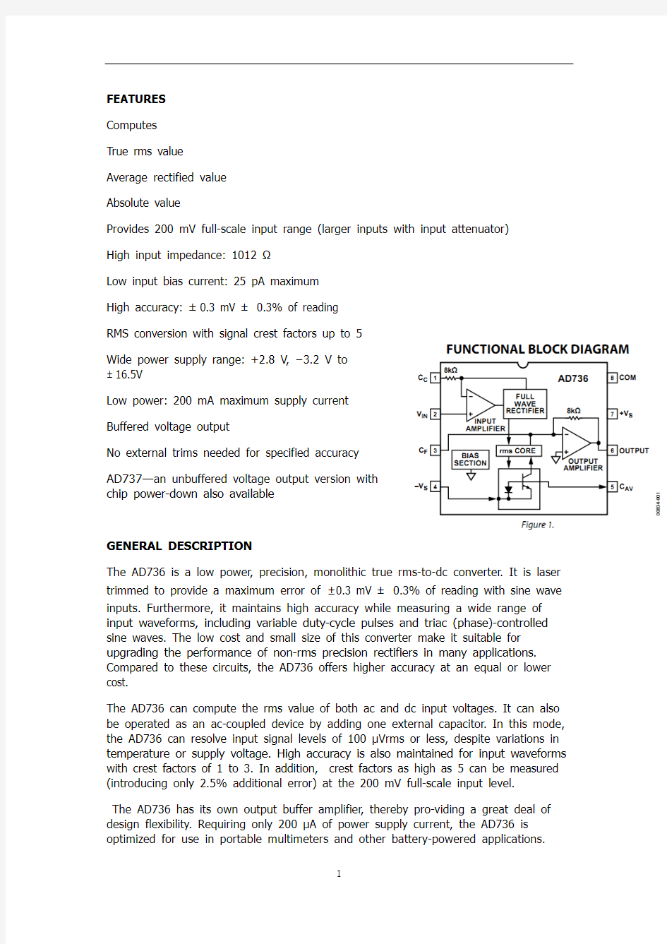
As shown by Figure 18, the AD736 has five functional subsections: the input amplifier, full-wave rectifier (FWR), rms core, output amplifier, and bias section. The FET input amplifier allows both a high impedance, buffered input (Pin 2) and a low impedance, wide dynamic range input (Pin 1). The high impedance input, with its low input bias current, is well suited for use with high impedance input attenuators. The output of the input amplifier drives a full-wave precision rectifier that, in turn, drives the rms core. The essential rms operations of squaring, averaging, and square rooting are performed in the core using an external averaging capacitor, C AV. Without C AV, the rectified input signal travels through the core unprocessed, as is done with the average responding connection (see Figure 19).
A final subsection, an output amplifier, buffers the output from the core and allows optional low-pass filtering to be performed via the external capacitor, CF, which is connected across the feedback path of the amplifier. In the average responding connection, this is where all of the averaging is carried out. In the rms circuit, this additional filtering stage helps reduce any output ripple that was not removed by the averaging capacitor, C AV.
TYPES OF AC MEASUREMENT
The AD736 is capable of measuring ac signals by operating as either an average responding converter or a true rms-to-dc converter. As its name implies, an average
responding converter computes the average absolute value of an ac (or ac and dc) voltage or current by full-wave rectifying and low-pass filtering the input signal; this approximates the average. The resulting output, a dc average level, is scaled by
adding (or reducing) gain; this scale factor converts the dc average reading to an rms equivalent value for the waveform being measured. For example, the average absolute value of a sine wave voltage is 0.636 times V PEAK; the corresponding rms value is 0.707 ×V PEAK. Therefore, for sine wave voltages, the required scale factor is 1.11 (0.707/0.636).
In contrast to measuring the average value, true rms measurement is a universal language among waveforms, allowing the magnitudes of all types of voltage (or current) waveforms to be compared to one another and to dc. RMS is a direct measure of the power or heating value of an ac voltage compared to that of a dc voltage; an ac signal of 1 V rms produces the same amount of heat in a resistor as a 1 V dc signal.
Mathematically, the rms value of a voltage is defined (using a simplified equation) as
This involves squaring the signal, taking the average, and then obtaining the square root. True rms converters are smart rectifiers; they provide an accurate rms reading regardless of the type of waveform being measured. However, average responding converters can exhibit very high errors when their input signals deviate from their precalibrated waveform; the magnitude of the error depends on the type of waveform being measured. For example, if an average responding converter is calibrated to measure the rms value of sine wave voltages and then is used to measure either symmetrical square waves or dc voltages, the converter has a computational error 11% (of reading) higher than the true rms value (see Table 4).
CALCULATING SETTLING TIME USING FIGURE 16
Figure 16 can be used to closely approximate the time required for the AD736 to settle when its input level is reduced in amplitude. The net time required for the rms converter to settle is the difference between two times extracted from the graph (the initial time minus the final settling time). As an example, consider the following conditions: a 33 μF averaging capacitor, a 100 mV initial rms input level, and a final (reduced) 1 mV input level. From Figure 16, the initial settling time (where the 100 mV l ine intersects the 33 μF line) is approximately 80 ms.
The settling time corresponding to the new or final input level of 1 mV is approximately 8 seconds. Therefore, the net time for the circuit to settle to its new value is 8 seconds minus 80 ms, which is 7.92 seconds. Note that because of the smooth decay characteristic inherent with a capacitor/diode combination, this is the total settling time to the final value (that is, not the settling time to 1%, 0.1%, and so on, of the final value). In addition, this graph provides the worst-case settling time because the AD736 settles very quickly with increasing input levels.
RMS MEASUREMENT—CHOOSING THE OPTIMUM VALUE FOR CAV Because the external averaging capacitor, C AV, holds the rectified input signal during rms computation, its value directly affects the accuracy of the rms measurement, especially at low frequencies. Furthermore, because the averaging capacitor appears across a diode in the rms core, the averaging time constant increases exponentially as the input signal is reduced. This means that as the input level decreases, errors due to nonideal averaging decrease, and the time required for the circuit to settle to the new rms level increases. Therefore, lower input levels allow the circuit to perform better (due to increased averaging) but increase the waiting time between measurements. Obviously, when selecting C AV, a trade-off between computational accuracy and settling time is required.
RAPID SETTLING TIMES VIA THE AVERAGE RESPONDING CONNECTION Because the average responding connection shown in Figure 19 does not use the C AV averaging capacitor, its settling time does not vary with the input signal level. It is determined solely by the RC time constant of CF and the internal 8 kΩ resistor in the ou tput amplifier’s feedback path.
DC ERROR, OUTPUT RIPPLE, AND AVERAGING ERROR
Figure 20 shows the typical output waveform of the AD736 with a sine wave input applied. As with all real-world devices, the ideal output of VOUT = VIN is never achieved exactly. Instead, the output contains both a dc and an ac error component. As shown in Figure 20, the dc error is the difference between the average of the output signal (when all the ripple in the output is removed by external filtering) and the ideal dc output. The dc error component is therefore set solely by the value of the averaging capacitor used. No amount of post filtering (that is, using a very large CF) allows the output voltage to equal its ideal value. The ac error component, an output ripple, can be easily removed by using a large enough post filtering capacitor, CF. In most cases, the combined magnitudes of both the dc and ac error components need to be considered when selecting appropriate values for Capacitor CAV and Capacitor CF. This combined error, representing the maximum uncertainty of the measurement, is termed the averaging error and is equal to the peak value of the output ripple plus the dc error.
As the input frequency increases, both error components decrease rapidly; if the input frequency doubles, the dc error and ripple reduce to one quarter and one half of their original values, respectively, and rapidly become insignificant.
AC MEASUREMENT ACCURACY AND CREST FACTOR
The crest factor of the input waveform is often overlooked when determining the accuracy of an ac measurement. Crest factor is defined as the ratio of the peak signal amplitude to the rms amplitude (crest factor = V PEAK/V rms). Many common waveforms, such as sine and triangle waves, have relatively low crest factors (≤2). Other waveforms, such as low duty-cycle pulse trains and SCR waveforms, have high crest factors. These types of waveforms require a long averaging time constant (to average out the long periods between pulses). Figure 8 shows the additional error vs. the crest factor of the AD736 for various values of C AV.
APPLICATIONS
CONNECTING THE INPUT
The inputs of the AD736 resemble an op amp, with noninverting and inverting inputs. The input stages are JFETs accessible at Pin 1 and Pin 2. Designated as the high impedance input, Pin 2 is connected directly to a JFET gate. Pin 1 is the low impedance input because of the scaling resistor connected to the gate of the second JFET. This gate-resistor junction is not externally accessible and is servo-edto the voltage level of the gate of the first JFET, as in a classic feedback circuit. This action results in the typical 8 kΩ input impedance referred to ground or reference level. This input structure provides four input configurations as shown in Figure 21, Figure 22, Figure 23, and Figure 24. Figure 21 and Figure 22 show the high impedance configurations, and Figure 23 and Figure 24 show the low impedance connections used to extend the input voltage range.
中文翻译
运算
真有效值RMS
平均整流值
绝对值
提供满量程200mV范围内输入电压(较大输入的输入衰减器)
高输入阻抗:1012Ω
低的输入偏置电流:25 pA最大值
精度高:±0.3 mV±0.3%的读入
波顶因数的有效值转换提升到5
宽供电范围:+ 2.8V,?3.2V到16.5 V
低功率:最大200mA就可正常运行
缓冲输出电压
没有外部协议需要规定准确性
AD737-是一个芯片断电也可使用的非缓冲电压输
出的版本
总体描述
AD736是一个低功率、精密、真有效值单块集成
电路的直流转换器。它是经过激光修正提供一个
最大误差±0.3 mV±0.3%的读如与正弦波的输入。此外,它在很宽的范围内测量输入波形仍能确保高精度,输入波形,包括脉冲占空比可变和相控正弦波。这个芯片低成本、体积小使它很方便在非有效值精密整流器在许多应用里有了很大的提升。比较这些芯片, AD736能提供更高的精确度以相同或更低的成本。
AD736可以计算交流电和直流电两种输入电压的有效值。它也可以添加一个外部电容器作为一个交流耦合的操作设备。在这种情况下, AD736可以解决输入信号有效值等于或少于100uV,即使温度和电压变化。高精度也保证输入的波形在1到3的峰值因子。此外,高达5波顶因数可以测量(引起附加的误差仅为2.5%)满量程200mV的水平。
AD736有它自己的输出缓冲放大器,从而大大提高设计的灵活性。只需要200μA 供电电流, AD736使便携式万用表和其他电池驱动的应用得到优化。
AD736允许两个信号输入端子可以选择:一个高阻抗场效应管输入(1012Ω)直接接口与高Z输入衰减器和低阻抗输入(8 kΩ),这样可以允许测量300mV输入值从最低的电源电压+ 2.8 V,?3.2 V。两个输入可以是使用单端或双端。
AD736有1%的错误读入带宽,超过10KHZ的输入振幅从20 mV有效值到200mV 有效值然而只消耗1 mW。
AD736有四个性能等级
AD736J和AD736K的额定等级是在0°到+ 70°C、20°C到?85°C商业级温度范围。
AD736A和AD736B的额定等级在40°到?85°C 工业级温度范围。
这个AD736是可利用的在三种低成本、8脚:PDIP,SOIC,CERDIP封装。
产品亮点
1.AD736能够计算平均矫正值、绝对值、真有效值等各种输入信号。
2. AD736只需一个外部组件,一个平均电容、就可以进行真有效值的测量。
3.低功耗1 mW使AD736适合许多电池驱动的应用。
4.一个高阻抗1012Ω的输入,当输入与衰减器连接时不需要外部的缓冲。
5.一个低阻抗的输入可供那些需要一个输入信号达到300 mV有效值在低电压下运行的应用。
规格
使用温度25°C±5 V、交流耦合 1KHZ正弦波输入,除非另有注明。说明书是在大胆的测试所有的产品单元后完成的。这些测试结果用于计算出厂质量。
超过最大额定值可能对设备造成永久性的损坏。这是额定值仅供参考,在高于额定值或其他的环境下设备的功能正常运行是不可取的。在最大额定值下使用,可能影响器件的可靠性。
工作原理
如图18所示,AD736有五个功能分段:输入放大器,全波整流器(FWR)、有
效值的核心、输出放大器、偏压部分。若场效应管输入放大器都允许的高阻抗,缓冲输入(Pin 2)和一个低阻抗、宽动态范围输入(Pin 1)。高阻抗输入,以其低的输入偏置电流,很适合使用高阻抗输入衰减器。
输入放大器的输出驱动全波精密整流器,进而带动有效值核心。基本的有效值操作就是平方,平均值,开平方在内部核心运行,使用一个外部平均电容器,C AV 。没有C AV ,整流后的输入信号穿越核心未被处理,由于已经完成平均响应连
接 (参见图19)。
最后一节、输出放大器、缓冲器输出从核心允许可选择低通滤波通过外部
电容器、CF 连接通过反馈放大器。在平均响应的联系,在这里所有的平均值运算被执行。在有效值电路中,该附加滤波阶段有助于减少输出信号中没有被平均电容过滤掉的脉动。
交流测量的类型
AD736能够测量交流信号通过操作要么是平均响应整流器或一个真有效值
的直流转换器。正如其名字所示,一个平均响应整流器计算交流电压得平均绝对值(或交流和直流)或者当前的全波整流或低通滤波输入信号,这个接近平均值。
输出结果,一个直流平均等级,按增加(或减少)增益来平衡;这种平衡因素转换的直流平均读入到一个真有效值等价于波形的测量。例如,一个正弦波电压的
平均绝对值是V
PEAK 0.636倍,相应的有效值是0.707×V
PEAK
。因此,对于正弦波电
压,所需的平衡因素是1.11(0.707/0.636)。
与测量平均值形成对比,真有效值的波形测量是一种世界通用方式,允许选择所有类型的电压(或电流)波形被比作一个到另一个和到直流。
有效值就是在相同的电阻上分别通以直流电流和交流电流,经过一个交流周期的时间,它们在电阻上所损失的电能相等。1V的交流与1V的直流在同一电阻上产生相同的热量。
数学的均方根值电压值的定义(使用一个简化方程)
这包括把信号平方,做平均值,然后在做平方根的计算。
真有效值的转换器是灵巧的整流器;他们提供一个准确的真有效值读取无论是哪类波形的测量。然而,平均响应转换器当他们的输入信号偏离事先标定的波形会出现误差;产生误差的大小取决于波形的被测形式。例如,如果一个平均响应转换器被校准去测量正弦波电压,然后又用于测量对称方波和直流电压,转换器就会产生(读入)高于真有效值11%的计算误差(见表4)。
计算稳定时间使用图16
图16可以用来得到粗略的估计AD736解决输入电平振幅下降所需的时间。真有效值转换器来解决两次提取图形之间的差别所需的净时间 (初始时间减去最终稳定时间)。例如,考虑以下条件: 一个33μF平均电容器,一个初始有效值为100mV的输入电平,和一个最终(减少)1 mV输入电平。从图16,初步建立时间(这里的100mV的线与33μF的线相交)大约是80毫秒。
相应的到达新的或最终输入的1 mV电平所需的稳定时间约为8秒。因此,电路来解决新值的净时间是8秒减80毫秒,即7.92秒。注意到电容器/二极管组合所固有的衰减平滑特性,这是总稳定时间到最终值(即不是稳定时间到
1%,0.1%,等等,最终值)。此外,本图提供了最坏情况的稳定时间,是因为AD736处理递增的输入电平非常迅速。
CAV有效值(RMS)测量的最佳选择
由于外部平均值电容器CAV,在有效值计算时保存整流输入信号 ,其值直接影响有效值的测量精度,特别对于低频来说。此外,因为平均电容器在有效值核心穿过一个二极管。当输入信号减小时,平均时间常数以指数形式增加。这意味着只要输入电压降低,误差由于非理想的平均而值减小 ,而电路所需处理新的有效值电压的时间增加了。因此,低输入电平使电路工作的更好(由于平均值增加),增加了测量操作时的等待时间。很明显,当选择了CAV,精确计算与需要到达的稳定时间是一种平衡关系。
通过的平均响应连接的快速建立时间
由于在图19展示出的平均响应关系没有使用CAV平均电容器,其稳定时间不随输入信号电平变化。它仅由RC时间常数的CF和内部8 kΩ电阻在输出放大器的反馈路径上而决定。
直流误差、输出的波纹,和平均误差
图20显示了典型的AD736正弦输入的输出波形应用。所有都是真实的设备,理想的输出VOUT = VIN是永远不能达到这样的。相反,输出既含有直流输和交流误差的组成部分。如图20时,直流误差是区别于平均输出信号(当所有的输出脉动都被外部滤波掉了)和理想的直流输出。直流误差的组成仅仅是平均值由于电容的使用。即使再多的后置滤波(也就是用一个非常大的CF)允许输出电压等于理想值。交流误差组成,一个输出脉动,能够被很容易被消除通过使用一个足够大的滤波电容器、CF。在大多数情况下,直流和交流误差的成分需要被考虑当选
和电容器CF的值时。这综合误差,代表着最大的不确定度量,择合适的电容器C
AV
是所谓的平均误差它等于输出脉动的峰值加上直流误差。
当输入频率的升高,两者误差部分迅速减少;如果输入频率加倍,直流误差和脉动减小到四分之一和原始值的一半,迅速成为无关紧要的因素。
交流测量精度和振幅因数
当决定一个交流测量的精确度输入波形的振幅因数常常被忽视。振幅因数
/ V rms)。许多常被定义为最大信号振幅与有效值振幅之比 (振幅因数= V
PEAK
见的波形,如正弦波和三角波,有相对较低的振幅因数(≤2)。其他波形,如低频宽比脉冲序列和可控硅波形,具有高振幅因数。这些类型的波形需要很长的平均时间常数(在脉冲之间需要很长的周期达到最终的平衡)。图8显示附加的误差对
值的AD736振幅因数。
比,对于各种各样的C
AV
应用
输入的连接
AD736的输入类似一个带着同向和反向的运算放大器。输入级是结型场效应
管(JFET)可以由1脚和2脚输入。指定为高阻抗输入、脚2直接连接到结型场效应管(JFET)门。脚1是低阻抗输入因为缩放电阻连接到第二个结型场效应管(JFET)门。门电阻没有在外部连接,是不容易servo-ed外部的电压水平的门,第一JFET,像一个经典的反馈电路。这个功能导致典型的8 kΩ输入阻抗涉及到地或参考电平。该输入装置提供了四个输入配置如图21,图22,图23,图24。图21图22展示高阻抗配置,图23和图24展示低阻抗关系用于扩展输入电压范围。
外文文献原文+译文 原文 The study on the design of neuter clothing H ous e W Abstract Social and economic development, social thought, opening up and the progress of science and technology, men and women style presented the diversified pattern of neuter the fuzzy gender differences in style, from the beginning of non-mainstream des ign till n ow has develop ed i nt o on e of the mains t ream fas hi on d es ign style. Fashion brands have launched in recent years, the neutral flavor of fashion, neuter clothing market share of more and more, neutral fashion, with its broad group of sex leads the urban street fashion. Neutralization of free and open way of life style, gave people a comfortable and enjoyable. K ey words: Neut e r; Cl ot hing; Gender roles; Design 1 Introduction The beginning of the 20th century the rise of the feminist movement, make the neutral clothing as a kind of style into the line of sight of people. In the 90 s, the neutral clothing has used by each big brand clothing as one of the fashionable e lement s, s uc h a s dust coa t w i th a ne ut ral style, s ui ts, t-shirt s and j e ans have bec om e people like everyday clothes. Neuter clothing style is a simple, pure; reject all multifarious mincing, personalized style. As a special kind of clothing style, neuter clothing fashion has been intensified in the social life, so it is necessary for us to study the clothing neutralization phenomenon, to study its causes and the development of sociology. This article mainly from the sociological association as well as the relationship between men and women clothing and gender status in the society, which is based on analyzing the change of the study the social basis of the neutral clothing appear; Again from the social system, economic development, cultural trend and fashion designers to the influence of the neutral clothing style, etc., it is concluded that the neuter clothing phenomenon is the development of social consciousness, the sexual role transformation, the new clothing design trends are affecting the results.
Load and Ultimate Moment of Prestressed Concrete Action Under Overload-Cracking Load It has been shown that a variation in the external load acting on a prestressed beam results in a change in the location of the pressure line for beams in the elastic range.This is a fundamental principle of prestressed construction.In a normal prestressed beam,this shift in the location of the pressure line continues at a relatively uniform rate,as the external load is increased,to the point where cracks develop in the tension fiber.After the cracking load has been exceeded,the rate of movement in the pressure line decreases as additional load is applied,and a significant increase in the stress in the prestressing tendon and the resultant concrete force begins to take place.This change in the action of the internal moment continues until all movement of the pressure line ceases.The moment caused by loads that are applied thereafter is offset entirely by a corresponding and proportional change in the internal forces,just as in reinforced-concrete construction.This fact,that the load in the elastic range and the plastic range is carried by actions that are fundamentally different,is very significant and renders strength computations essential for all designs in order to ensure that adequate safety factors exist.This is true even though the stresses in the elastic range may conform to a recognized elastic design criterion. It should be noted that the load deflection curve is close to a straight line up to the cracking load and that the curve becomes progressively more curved as the load is increased above the cracking load.The curvature of the load-deflection curve for loads over the cracking load is due to the change in the basic internal resisting moment action that counteracts the applied loads,as described above,as well as to plastic strains that begin to take place in the steel and the concrete when stressed to high levels. In some structures it may be essential that the flexural members remain crack free even under significant overloads.This may be due to the structures’being exposed to exceptionally corrosive atmospheres during their useful life.In designing prestressed members to be used in special structures of this type,it may be necessary to compute the load that causes cracking of the tensile flange,in order to ensure that adequate safety against cracking is provided by the design.The computation of the moment that will cause cracking is also necessary to ensure compliance with some design criteria. Many tests have demonstrated that the load-deflection curves of prestressed beams are approximately linear up to and slightly in excess of the load that causes the first cracks in the tensile flange.(The linearity is a function of the rate at which the load is applied.)For this reason,normal elastic-design relationships can be used in computing the cracking load by simply determining the load that results in a net tensile stress in the tensile flange(prestress minus the effects of the applied loads)that is equal to the tensile strength of the concrete.It is customary to assume that the flexural tensile strength of the concrete is equal to the modulus of rupture of the
外文出处: 《Exploiting Software How to Break Code》By Greg Hoglund, Gary McGraw Publisher : Addison Wesley Pub Date : February 17, 2004 ISBN : 0-201-78695-8 译文标题: JDBC接口技术 译文: JDBC是一种可用于执行SQL语句的JavaAPI(ApplicationProgrammingInterface应用程序设计接口)。它由一些Java语言编写的类和界面组成。JDBC为数据库应用开发人员、数据库前台工具开发人员提供了一种标准的应用程序设计接口,使开发人员可以用纯Java语言编写完整的数据库应用程序。 一、ODBC到JDBC的发展历程 说到JDBC,很容易让人联想到另一个十分熟悉的字眼“ODBC”。它们之间有没有联系呢?如果有,那么它们之间又是怎样的关系呢? ODBC是OpenDatabaseConnectivity的英文简写。它是一种用来在相关或不相关的数据库管理系统(DBMS)中存取数据的,用C语言实现的,标准应用程序数据接口。通过ODBCAPI,应用程序可以存取保存在多种不同数据库管理系统(DBMS)中的数据,而不论每个DBMS使用了何种数据存储格式和编程接口。 1.ODBC的结构模型 ODBC的结构包括四个主要部分:应用程序接口、驱动器管理器、数据库驱动器和数据源。应用程序接口:屏蔽不同的ODBC数据库驱动器之间函数调用的差别,为用户提供统一的SQL编程接口。 驱动器管理器:为应用程序装载数据库驱动器。 数据库驱动器:实现ODBC的函数调用,提供对特定数据源的SQL请求。如果需要,数据库驱动器将修改应用程序的请求,使得请求符合相关的DBMS所支持的文法。 数据源:由用户想要存取的数据以及与它相关的操作系统、DBMS和用于访问DBMS的网络平台组成。 虽然ODBC驱动器管理器的主要目的是加载数据库驱动器,以便ODBC函数调用,但是数据库驱动器本身也执行ODBC函数调用,并与数据库相互配合。因此当应用系统发出调用与数据源进行连接时,数据库驱动器能管理通信协议。当建立起与数据源的连接时,数据库驱动器便能处理应用系统向DBMS发出的请求,对分析或发自数据源的设计进行必要的翻译,并将结果返回给应用系统。 2.JDBC的诞生 自从Java语言于1995年5月正式公布以来,Java风靡全球。出现大量的用java语言编写的程序,其中也包括数据库应用程序。由于没有一个Java语言的API,编程人员不得不在Java程序中加入C语言的ODBC函数调用。这就使很多Java的优秀特性无法充分发挥,比如平台无关性、面向对象特性等。随着越来越多的编程人员对Java语言的日益喜爱,越来越多的公司在Java程序开发上投入的精力日益增加,对java语言接口的访问数据库的API 的要求越来越强烈。也由于ODBC的有其不足之处,比如它并不容易使用,没有面向对象的特性等等,SUN公司决定开发一Java语言为接口的数据库应用程序开发接口。在JDK1.x 版本中,JDBC只是一个可选部件,到了JDK1.1公布时,SQL类包(也就是JDBCAPI)
华北电力大学科技学院 毕业设计(论文)附件 外文文献翻译 学号:121912020115姓名:彭钰钊 所在系别:动力工程系专业班级:测控技术与仪器12K1指导教师:李冰 原文标题:Infrared Remote Control System Abstract 2016 年 4 月 19 日
红外遥控系统 摘要 红外数据通信技术是目前在世界范围内被广泛使用的一种无线连接技术,被众多的硬件和软件平台所支持。红外收发器产品具有成本低,小型化,传输速率快,点对点安全传输,不受电磁干扰等特点,可以实现信息在不同产品之间快速、方便、安全地交换与传送,在短距离无线传输方面拥有十分明显的优势。红外遥控收发系统的设计在具有很高的实用价值,目前红外收发器产品在可携式产品中的应用潜力很大。全世界约有1亿5千万台设备采用红外技术,在电子产品和工业设备、医疗设备等领域广泛使用。绝大多数笔记本电脑和手机都配置红外收发器接口。随着红外数据传输技术更加成熟、成本下降,红外收发器在短距离通讯领域必将得到更广泛的应用。 本系统的设计目的是用红外线作为传输媒质来传输用户的操作信息并由接收电路解调出原始信号,主要用到编码芯片和解码芯片对信号进行调制与解调,其中编码芯片用的是台湾生产的PT2262,解码芯片是PT2272。主要工作原理是:利用编码键盘可以为PT2262提供的输入信息,PT2262对输入的信息进行编码并加载到38KHZ的载波上并调制红外发射二极管并辐射到空间,然后再由接收系统接收到发射的信号并解调出原始信息,由PT2272对原信号进行解码以驱动相应的电路完成用户的操作要求。 关键字:红外线;编码;解码;LM386;红外收发器。 1 绪论
计算机网络安全综述学生姓名:李嘉伟 学号:11209080279 院系:信息工程学院指导教师姓名:夏峰二零一三年十月
[摘要] 随着计算机网络技术的快速发展,网络安全日益成为人们关注的焦点。本文分析了影响网络安全的主要因素及攻击的主要方式,从管理和技术两方面就加强计算机网络安全提出了针对性的建议。 [关键词] 计算机网络;安全;管理;技术;加密;防火墙 一.引言 计算机网络是一个开放和自由的空间,但公开化的网络平台为非法入侵者提供了可乘之机,黑客和反黑客、破坏和反破坏的斗争愈演愈烈,不仅影响了网络稳定运行和用户的正常使用,造成重大经济损失,而且还可能威胁到国家安全。如何更有效地保护重要的信息数据、提高计算机网络的安全性已经成为影响一个国家的政治、经济、军事和人民生活的重大关键问题。本文通过深入分析网络安全面临的挑战及攻击的主要方式,从管理和技术两方面就加强计算机网络安全提出针对性建议。
二.正文 1.影响网络安全的主要因素[1] 计算机网络安全是指“为数据处理系统建立和采取的技术和管理的安全保护,保护计算机硬件、软件数据不因偶然和恶意的原因而遭到破坏、更改和泄漏”。计算机网络所面临的威胁是多方面的,既包括对网络中信息的威胁,也包括对网络中设备的威胁,但归结起来,主要有三点:一是人为的无意失误。如操作员安全配置不当造成系统存在安全漏洞,用户安全意识不强,口令选择不慎,将自己的帐号随意转借他人或与别人共享等都会给网络安全带来威胁。二是人为的恶意攻击。这也是目前计算机网络所面临的最大威胁,比如敌手的攻击和计算机犯罪都属于这种情况,此类攻击又可以分为两种:一种是主动攻击,它以各种方式有选择地破坏信息的有效性和完整性;另一类是被动攻击,它是在不影响网络正常工作的情况下,进行截获、窃取、破译以获得重要机密信息。这两种攻击均可对计算机网络造成极大的危害,并导致机密数据的泄漏。三是网络软件的漏洞和“后门”。任何一款软件都或多或少存在漏洞,这些缺陷和漏洞恰恰就是黑客进行攻击的首选目标。绝大部分网络入侵事件都是因为安全措施不完善,没有及时补上系统漏洞造成的。此外,软件公司的编程人员为便于维护而设置的软件“后门”也是不容忽视的巨大威胁,一旦“后门”洞开,别人就能随意进入系统,后果不堪设想。
文献出处:A Dehghani. The application of digital printing in fashion design [J]. International Journal of Clothing Science and Technology, 2015, 16(2): 263-271. 原文 The application of digital printing in fashion design A Dehghani Abstract The appearance of digital printing for textiles printing provides a new train of thought, digital printing with the current textile fabric printing a variety of requirements of the market of printing technology, including high quality printing precision, high efficiency of printing on reaction time and the printing of the diverse demand, these advantages directly promoted the digital ink jet printing in the rapid development of textile fabric printing direction. In this paper, the design method of the digital printing design of different style and means of decoration and design method in the fabrics for summary, it is concluded that digital printing design cuttings in fabric printing, clothing apparel printing method and the application of the traditional fabric secondary design and decorative effect. Through the above research, digital printing and garment design and garment style between the relationships between the shapes, thereby further to bring into full play the advantages of
Journal of Industrial Textiles https://www.doczj.com/doc/3917667289.html,/ Optimization of Parameters for the Production of Needlepunched Nonwoven Geotextiles Amit Rawal, Subhash Anand and Tahir Shah 2008 37: 341Journal of Industrial Textiles DOI: 10.1177/1528083707081594 The online version of this article can be found at: https://www.doczj.com/doc/3917667289.html,/content/37/4/341 Published by: https://www.doczj.com/doc/3917667289.html, can be found at:Journal of Industrial TextilesAdditional services and information for https://www.doczj.com/doc/3917667289.html,/cgi/alertsEmail Alerts: https://www.doczj.com/doc/3917667289.html,/subscriptionsSubscriptions: https://www.doczj.com/doc/3917667289.html,/journalsReprints.navReprints: https://www.doczj.com/doc/3917667289.html,/journalsPermissions.navPermissions: https://www.doczj.com/doc/3917667289.html,/content/37/4/341.refs.htmlCitations: - Mar 28, 2008Version of Record >>
外文翻译 专业机械设计制造及其自动化学生姓名刘链柱 班级机制111 学号1110101102 指导教师葛友华
外文资料名称: Design and performance evaluation of vacuum cleaners using cyclone technology 外文资料出处:Korean J. Chem. Eng., 23(6), (用外文写) 925-930 (2006) 附件: 1.外文资料翻译译文 2.外文原文
应用旋风技术真空吸尘器的设计和性能介绍 吉尔泰金,洪城铱昌,宰瑾李, 刘链柱译 摘要:旋风型分离器技术用于真空吸尘器 - 轴向进流旋风和切向进气道流旋风有效地收集粉尘和降低压力降已被实验研究。优化设计等因素作为集尘效率,压降,并切成尺寸被粒度对应于分级收集的50%的效率进行了研究。颗粒切成大小降低入口面积,体直径,减小涡取景器直径的旋风。切向入口的双流量气旋具有良好的性能考虑的350毫米汞柱的低压降和为1.5μm的质量中位直径在1米3的流量的截止尺寸。一使用切向入口的双流量旋风吸尘器示出了势是一种有效的方法,用于收集在家庭中产生的粉尘。 摘要及关键词:吸尘器; 粉尘; 旋风分离器 引言 我们这个时代的很大一部分都花在了房子,工作场所,或其他建筑,因此,室内空间应该是既舒适情绪和卫生。但室内空气中含有超过室外空气因气密性的二次污染物,毒物,食品气味。这是通过使用产生在建筑中的新材料和设备。真空吸尘器为代表的家电去除有害物质从地板到地毯所用的商用真空吸尘器房子由纸过滤,预过滤器和排气过滤器通过洁净的空气排放到大气中。虽然真空吸尘器是方便在使用中,吸入压力下降说唱空转成比例地清洗的时间,以及纸过滤器也应定期更换,由于压力下降,气味和细菌通过纸过滤器内的残留粉尘。 图1示出了大气气溶胶的粒度分布通常是双峰形,在粗颗粒(>2.0微米)模式为主要的外部来源,如风吹尘,海盐喷雾,火山,从工厂直接排放和车辆废气排放,以及那些在细颗粒模式包括燃烧或光化学反应。表1显示模式,典型的大气航空的直径和质量浓度溶胶被许多研究者测量。精细模式在0.18?0.36 在5.7到25微米尺寸范围微米尺寸范围。质量浓度为2?205微克,可直接在大气气溶胶和 3.85至36.3μg/m3柴油气溶胶。
译文(一) THE ACCOUNTING REVIEW V ol. 83, No. 3 2008 pp. 823–853 市场参与者的杜邦分析的使用 马克?t?Soliman 华盛顿大学 文摘:杜邦分析,一种常见的财务报表分析,依靠于净营业资产收益率的两个乘法组件:利润率和资产周转率。这两个会计比率衡量不同的构造。因此,有不同的属性。之前的研究已经发现,资产周转率的变化是未来收益的变化正相关。本文全面探讨了杜邦组件和沿着三个维度有助于文学。首先,本文有助于财务报表分析文献,发现在这个会计信息信号实际上是增量学习会计信号在先前的研究在预测未来收益。其次,它有助于文学在股票市场上使用的会计信息通过检查眼前和未来的股本回报投资者应对这些组件。最后,它增加了分析师的文献处理会计信息的再次测试直接和延迟反应的分析师通过同期预测修正以及未来预测错误。一致的跨市场加入者的两组,结果表明是有用的信息就是明证杜邦组件和股票收益之间的联系以及维度分析师预测。然而,我发现预测未来预测错误和异常返回信息处理表明似乎没有完成。平均水平,分析表明杜邦组件代表增量和可行的操作特征信息的公司。 关键词:财务报表分析、杜邦分析、市场回报、分析师预估。 数据可用性:在这项研究中使用的数据是公开的来源显示的文本。 在本文中,我分析杜邦分析中包含的信息是否与股市回报相关和分析师预测。之前的研究文档组件从杜邦分析,分解的净营业资产收益率为利润率和资产周转率,有解释力对未来盈利能力的变化。本文增加了文献综合研究投资者和分析师反应杜邦组件三个维度。首先,它复制先前记录的预测能力和检查是否健壮和增量其他预测已经考虑在文学的存在。其次,它探讨了使用这些组件的股市投资者通过观察同生和未来收益。在同时代的长窗协会和短时期限信息测试,结果显示积极联系杜邦组件和股本回报率。但小未来异常返回交易策略显示的信息可能不完整的处理。最后,检查当前预测修正由卖方分析师和未来的预测错误。尽管他们似乎修改他们的预测未来收益与这些杜邦组件中的信息一致,修订似乎不完整就是明证可预测的未来预测错误。一致的市场参与者,在两组同期结果表明,信息是有用的,但是未来的测试表明,信息处理似乎没有完成。 由金矿和笔者(2001)提供了一个使用剩余收益的股票估值方法框架,给出了一个简单的财务比率分析的直接映射到股票估值。特别是他们用杜邦分析,分解公司的净营业资产收益率(RNOA)利润率(PM)和资产周转率(ATO)点的地方1。PM和ATO会计信号,测量不同结构对一个公司的业务2。PM 往往是来自定价权,如产品创新,产品定位,品牌知名度,先发优势和市场定位。ATO措施资产利用率和效率,通常来自于有效的利用财产,工厂和设备,有效的库存流程;和其他形式的资本管理工作3。 我们有理由期待竞争力量的影响这两个来源盈利能力不同。大的利润率通常吸引新进入者进入市场或快速模仿新思想从现有的竞争对手。由此产生的竞争导致高利润率回归正常水平,暗示更多暂时的利益。与利润不同,然而,竞争可能少威胁要部署一个有效的资产。更难以模仿另一个公司的高效生产流程因为这样模仿通常包括大型和昂贵的改革目前的工厂和操作。 1.具体来说,RNOA营业收入/平均净营业资产,PM营业收入/销售和ATO销售 /平均净营业资产。此后,点和ATO被称为“杜邦公司组成”。另一个常见的形式是分解罗伊(利润杠杆资产周转率)或(NI /产品销售/资产资产/股本)。讨论的“估值理论和RNOA”部分,我在分析使用RNOA为了专注于操作,因此抽象从公司的融资决策。 2.例如,阿伯克龙比和惠誉赚取高额利润通过出售used-looking服装被认为是时髦和青少年所要
文献信息: 文献标题:Evolution of Fashion Design in the Era of High-Tech Culture (高科技文化时代服装设计的演变) 国外作者:Galina Mihaleva,C.Koh 文献出处:《International Scholarly and Scientific Research and Innovation》,2016,10(7):2447-2451 字数统计:英文2079单词,11462字符;中文3549汉字 外文文献: Evolution of Fashion Design in the Era of High-Tech Culture Abstract Fashion, like many other design fields, undergoes numerous evolutions throughout the ages. This paper aims to recognize and evaluate the significance of advance technology in fashion design and examine how it changes the role of modern fashion designers by modifying the creation process. It also touches on how modern culture is involved in such developments and how it affects fashion design in terms of conceptualizing and fabrication. By comparing case studies, existing fashion design examples and crafting method experimentations; we then spot patterns in which to predict the direction of future developments in the field. A breakdown on the elements of technology in fashion design helps us understand the driving force behind such a trend. The results from explorations in the paper have shown that there is an observed pattern of a distinct increase in interest and progress in the field of fashion technology, which leads to the birth of hybrid crafting methods. In conclusion, it is shown that as fashion technology continues to evolve, their role in clothing crafting becomes more prominent and grows far beyond the humble sewing machine. Keywords: Fashion design, functional aesthetics, smart textiles, 3D printing. INTRODUCTION It is common knowledge that the environment we live in greatly influences the
毕业论文外文文献翻译 毕业设计(论文)题目关于企业内部环境绩效审计的研究翻译题目最高审计机关的环境审计活动 学院会计学院 专业会计学 姓名张军芳 班级09020615 学号09027927 指导教师何瑞雄
最高审计机关的环境审计活动 1最高审计机关越来越多的活跃在环境审计领域。特别是1993-1996年期间,工作组已检测到环境审计活动坚定的数量增长。首先,越来越多的最高审计机关已经活跃在这个领域。其次是积极的最高审计机关,甚至变得更加活跃:他们分配较大部分的审计资源给这类工作,同时出版更多环保审计报告。表1显示了平均数字。然而,这里是机构间差异较大。例如,环境报告的数量变化,每个审计机关从1到36份报告不等。 1996-1999年期间,结果是不那么容易诠释。第一,活跃在环境审计领域的最高审计机关数量并没有太大变化。“活性基团”的组成没有保持相同的:一些最高审计机关进入,而其他最高审计机关离开了团队。环境审计花费的时间量略有增加。二,但是,审计报告数量略有下降,1996年和1999年之间。这些数字可能反映了从量到质的转变。这个信号解释了在过去三年从规律性审计到绩效审计的转变(1994-1996年,20%的规律性审计和44%绩效审计;1997-1999:16%规律性审计和绩效审计54%)。在一般情况下,绩效审计需要更多的资源。我们必须认识到审计的范围可能急剧变化。在将来,再将来开发一些其他方式去测算人们工作量而不是计算通过花费的时间和发表的报告会是很有趣的。 在2000年,有62个响应了最高审计机关并向工作组提供了更详细的关于他们自1997年以来公布的工作信息。在1997-1999年,这62个最高审计机关公布的560个环境审计报告。当然,这些报告反映了一个庞大的身躯,可用于其他机构的经验。环境审计报告的参考书目可在网站上的最高审计机关国际组织的工作组看到。这里这个信息是用来给最高审计机关的审计工作的内容更多一些洞察。 自1997年以来,少数环境审计是规律性审计(560篇报告中有87篇,占16%)。大多数审计绩效审计(560篇报告中有304篇,占54%),或组合的规律性和绩效审计(560篇报告中有169篇,占30%)。如前文所述,绩效审计是一个广泛的概念。在实践中,绩效审计往往集中于环保计划的实施(560篇报告中有264篇,占47%),符合国家环保法律,法规的,由政府部门,部委和/或其他机构的任务给访问(560篇报告中有212篇,占38%)。此外,审计经常被列入政府的环境管理系统(560篇报告中有156篇,占28%)。下面的元素得到了关注审计报告:影响或影响现有的国家环境计划非环保项目对环境的影响;环境政策;由政府遵守国际义务和承诺的10%至20%。许多绩效审计包括以上提到的要素之一。 1本文译自:S. Van Leeuwen.(2004).’’Developments in Environmental Auditing by Supreme Audit Institutions’’ Environmental Management Vol. 33, No. 2, pp. 163–1721
毕业设计(论文) 外文翻译 题目西安市水源工程中的 水电站设计 专业水利水电工程 班级 学生 指导教师 2016年
研究钢弧形闸门的动态稳定性 牛志国 河海大学水利水电工程学院,中国南京,邮编210098 nzg_197901@https://www.doczj.com/doc/3917667289.html,,niuzhiguo@https://www.doczj.com/doc/3917667289.html, 李同春 河海大学水利水电工程学院,中国南京,邮编210098 ltchhu@https://www.doczj.com/doc/3917667289.html, 摘要 由于钢弧形闸门的结构特征和弹力,调查对参数共振的弧形闸门的臂一直是研究领域的热点话题弧形弧形闸门的动力稳定性。在这个论文中,简化空间框架作为分析模型,根据弹性体薄壁结构的扰动方程和梁单元模型和薄壁结构的梁单元模型,动态不稳定区域的弧形闸门可以通过有限元的方法,应用有限元的方法计算动态不稳定性的主要区域的弧形弧形闸门工作。此外,结合物理和数值模型,对识别新方法的参数共振钢弧形闸门提出了调查,本文不仅是重要的改进弧形闸门的参数振动的计算方法,但也为进一步研究弧形弧形闸门结构的动态稳定性打下了坚实的基础。 简介 低举升力,没有门槽,好流型,和操作方便等优点,使钢弧形闸门已经广泛应用于水工建筑物。弧形闸门的结构特点是液压完全作用于弧形闸门,通过门叶和主大梁,所以弧形闸门臂是主要的组件确保弧形闸门安全操作。如果周期性轴向载荷作用于手臂,手臂的不稳定是在一定条件下可能发生。调查指出:在弧形闸门的20次事故中,除了极特殊的破坏情况下,弧形闸门的破坏的原因是弧形闸门臂的不稳定;此外,明显的动态作用下发生破坏。例如:张山闸,位于中国的江苏省,包括36个弧形闸门。当一个弧形闸门打开放水时,门被破坏了,而其他弧形闸门则关闭,受到静态静水压力仍然是一样的,很明显,一个动态的加载是造成的弧形闸门破坏一个主要因素。因此弧形闸门臂的动态不稳定是造成弧形闸门(特别是低水头的弧形闸门)破坏的主要原是毫无疑问。
A Case Study of Pattern-based Software Framework to Improve the Quality of Software Development Chih-Hung Chang, Chih-Wei Lu Dept. of Information Management, Hsiuping Institute of Technology No.11, Gongye Rd., Dali City, Taichung County, Taiwan(R.O.C.) 886-4-24961123 ext 3112 {chchang,cwlu}@ https://www.doczj.com/doc/3917667289.html,.tw William C. Chu Dept. of Computer Science and Information Engineering, Tunghai University No.181, Sec. 3, Taichung Port Rd.,Taichung City, Taiwan (R.O.C.) 886-4-23508983 cchu@https://www.doczj.com/doc/3917667289.html,.tw Nien-Lin Hsueh Dept. of Information Engineering and Computer Science, Feng Chia University No. 100 Wenhwa Rd., Taichung, Taiwan (R.O.C.) 886-4- 24517250 ext 3773 nlhsueh@https://www.doczj.com/doc/3917667289.html,.tw Chorng-Shiuh Koong Dept. of Computer and Information Science, Taichung University No.140, Ming-Sheng Rd., Taichung City, Taiwan (R.O.C.) 886-4-22183804 csko@https://www.doczj.com/doc/3917667289.html,.tw ABSTRACT In recent years, development of the software industry and demand for software systems have increased rapidly, but developers often does not know whose suggestion to follow regarding methodologies of software engineering. One reason for that is the difficulty in applying new software engineering technologies. Developers take a long time to train. Another reason is the difficulty in integrating CASE toolsets. So many indeterminate factors make the development process more and more complex. On the other hand, software development is too customized, and software reuse is difficult. T he reasons above are the cause for software development and maintenance to become more complex and difficult to control. In this paper we explore the importation of a software pattern-based framework, and the development of an ERP/support chain system. Based on software patterns, developers can separate development and business so as to reduce problems caused by the developer’s lack of business experience. T he quality of the product can thus be enhanced, software development costs be reduced, and software maintenance be improved. Keywords Design Pattern, Framework, Software Development Process, XML 1.INTRODUCTION In Object-Oriented T echnology, the property of inheritance allows software components to be reused, which can obviously reduce the cost of software development. For this reason, to produce a highly reusable software component is an important goal of software engineering. However, programmers are usually focused on code reuse while ignoring design reuse. Design patterns provide a clear concept of design structure by describing the relationships of inheritance and reference between components of the system. Design patterns are a series of familiar usages and constructions utilized throughout system design. Design patterns allow rapid coding of certain components by following certain patterns of steps. T his can improve the documentation and maintenance of existing systems by providing an explicit specification of class, object interactions and their underlying intents. One of the main purposes of design patterns is to help software engineers to understand the common characteristics of software objects/components in specialized domain. In recent years, due to the development and maturation of WWW and Java [14] technologies, many applications are now web applications or leaning in that direction. Many software concepts are utilized for the web as well, such as Design Patterns and Frameworks. The Apache Struts [12] and Spring Framework [13] are both open source frameworks used to address and reduce the complexity of developing an enterprise application. T he advantage of using a framework is the layered architecture it provides. Layered architecture allowed users to choose the component desired, while also providing the integration framework when developing application using J2EE. T hese developing web concepts can facilitate the development of web applications. However, these very useful tools and concepts lack a systematic organization. We hope to use these open source software technologies to develop a software framework which can be applied to web application. T his should solve the problem of web applications lacking a good structure, while through applying these open source software technologies, software development costs will be reduced. Furthermore, a guideline for programmers who wants to use these open source technologies will be provided. This paper is organized as follows: In the next section, we discuss works related to our project; in section 3, the open source technologies used in the paper and the system implementation will be described; Section 4 is a sample experiment. T he conclusion is given in section 5.