microsd_card_spec
- 格式:pdf
- 大小:755.36 KB
- 文档页数:25
|卡基础知识SDGet新技能卡便是当下应用SD无论玩相机还是摄像机,数据都得记录在储存卡上,而Ⅲ,从UHS-最广,最受关注的储存卡。
从规范1.0到规范5.1,从class10到Ⅱ和闪迪维刚Premier ONE系列(以及雷克沙Professional 2000x UHS-(写SF-G Ⅱ,三者写入速度同是260MB/s)到索尼系列Extreme PRO UHS-卡在不断提高自身性能以迎合SD入速度达到299MB/s,世界最快),都表明大众需要。
卡各式各样不同写入速度卡厂商和品牌中,在那么,在如此琳琅满目的SDSD 卡呢?和储存量规格中,我们如何保证正确的选择了SDSD卡进阶历程▲SD卡家族,三种尺寸满足你的需求micro SD 到mini SD到SD从卡卡、micro SD卡划分为:SD卡、mini SD根据外型,可以大致将SD是最大的一种,今SD卡)。
不同设备使用不同尺寸的SD卡。
标准TF(旧称这种卡有标准卡,天市面上大多数消费级数字相机和摄像机均使用此标准的SD卡,这种卡原本是为笔记本电脑而设SDMini SD卡小于标准的“缺角”设计。
是最SD 卡,现在非常少见了。
Micro SD计,但由于笔记本已兼容标准尺寸的大多数手机支持此卡,卡,TF小的一种SD卡标准,也就是通常意义上我们说的。
它们也广泛应用于其他设备,比如Ipad卡SD不同形状的▲.▲不同形状的SD卡的详细参数从SD到SDHC到SDXC,从class10到UHS-Ⅰ、UHS-Ⅱ到UHS-Ⅲ谢天谢地,SDA(SD卡协会)不断推出新的规范和新的标准,让SD卡的性能直线提升,使其在速度和容量上跟上甚至超过主机发展的节奏。
根据SD卡的容量,SD卡分为SD、SDHC(SD High Capacity)、SDXC(SD Extended Capacity)三种标准。
而当下SDHC卡和SDXC卡才是市面上的扛把子,SD 卡由于容量太小处于淘汰趋势,市面上几近消失。

O5MDP1Revision History1.Introduction (5)1.1. Overview (5)1.2. Specification (6)1.3. Applications of O5MDP1 (7)2.Product Description (8)2.1. Contents (8)2.2. Product Preview (8)2.3. Physical description (9)2.3.1. External View (9)2.3.2. Dimension (9)2.3.3. External Connector (10)2.3.4. Factory Default Switch (10)2.4. Functional Description (11)3.On Site Installation (13)4.Getting Started (14)4.1. PC Requirement (14)4.2. Quick Installation Guide (14)4.2.1. Connect PC and O5MDP1 to network. (14)4.2.2. Install Speco-NVR and set IP parameters on O5MDP1 (15)4.2.3. Remote video connection to O5MDP1 (17)4.2.4. Additional settings through connection to the Admin Page (19)4.2.5. Panoramic viewing through Speco-NVR (20)5.Trouble Shooting (21)5.1. No power is applied (21)5.2. Cannot connect to the Video (22)5.3. Windows Vista or Windows 7 (23)5.4. Technical Assistance (26)Appendix A – Important Notice in Exchanging SD Card (Micro SD) (27)1.1. OverviewThe O5MDP1 is panoramic IP camera offering panoramic view of 360︒ or 180︒ for covering entire surveillance area with a single IP camera. 5 Mega Pixel image from Panomorph camera module can replace up to 4 PTZ cameras and 5 fixed cameras. It enables real time transmission of synchronized video of up to 2,592x1,944(10fps) video and audio data. Remote clients can connect to O5MDP1 for the real time video/audio data through various client solutions running on PC or smart device. Real time 2-way communication is available through bidirectional audio communication feature.Designed to be a stand-alone streaming audio & video transmission device, O5MDP1 can be applied to various application area such as video security, remote video monitoring, distance education, video conference or internet broadcasting system.Vandal proof and weather proof housingwillextendtheapplication area to harsh environment of wide temperature range. Embedded PoE (Power over Ethernet, IEEE 802.3af) will enable the owner to reduce the total cost of ownership by reducing on-site wiring works for the installation.Original VideoPTZ modePan/Tilt/Zoom ControlQuad modeEach sub-screen with independent Pan/Tilt/Zoom replaces 4 independent PTZ cameras.Perimeter mode2 x180︒views with panning control for ceiling mount. One 180︒ views for wallmount. Replaces two 180︒ cameras..Up to 5 crop windows of 320 x 240. Replaces up to 5 fixed cameras.1.3. Applications of O5MDP1•Security surveillance (buildings, stores, manufacturing facilities, parking lots, banks, government facilities, military, etc.)•Remote monitoring (hospitals, kindergartens, traffic, public areas, etc.)•eleconference (Bi-directional audio conference). Remote Learning, Internet broadcasting•Weather and environmental observation2.1. ContentsThe product package contains followings :12V DC Adaptor(Optional item) 2.2. Product PreviewMain Unit PC software to allocate an IPaddress to the IP CameraPC software to view and record theA/V streaming data transmitted from2.3. Physical description2.3.1. External ViewFigure 2-1. External view of O5MDP12.3.2. DimensionUnit : mmFigure 2-2. Dimension2.3.3. External ConnectorFigure 2-3. Connector for external connection2.3.4. Factory Default SwitchFactory default switch is provided for returning the IP camera to factory default state. Unscrew the cover to access the switch. There are two functions assigned to factory default switch.1. Returning to Factory Default State : Press the switch about 5 seconds while power is applied toreturn to factory default state.2. Safe Removal of Micro-SD Card : Press the switch for 1 second to unmount Micro-SD Card for saferemoval.Figure 2-4. Factory Default switch and Micro-SD Card slotLine Output2.4. Functional Description•Power : Power input for supplying 12V DC, 1A power.Caution : If O5MDP1 is powered by PoE, do not plug in DC Jack with active DC power into DC power connector.• Network (LAN)100Mbps Ethernet connector (RJ-45) with PoE standard (802.3af). LED on the Ethernet connector shows the status of O5MDP1 as the followings:- Status LED (It will be lit in green or red depending on the status)① Green : Green color indicates that the camera is in normal operation mode. Continuous greenindicates that data transmission is possible. Blinking green means that someone is connected to O5MDP1.② Red : Continuous or blinking red indicates that hardware is in abnormal condition.• Micro SD Card slotPlease insert SD memory card when you want to use SD memory card. In case of pulling out SD memory card, please push the SD card.• MIC/Line InputConnect external audio source or microphone.• Line OutputConnect speakers with built in amplifier. Audio from remote site is output through Line out in bi-directional audio mode.LED will be lit with red momentarily and it will be lit with green after a while when power is applied into O5MDP1• Relay OutputRelay output is provided for connecting alarm devices or for remote on/off control of devices such as light. Relay is normal open and it will be closed upon alarm annunciation or remote on. The relay is capable of switching 30V AC/DC, 2A . For the application which needs power switching beyond this limit, use additional relay switch as shown in the right of Figure 2-5.* Left : switching requirement below 30V, 2A* Right : switching requirement higher than 30V, 2A. Apply this connection when either voltage orcurrent exceed the limit.Figure 2-5. RELAY Output connection• Sensor InputConnect external alarm sensor. Examples of sensing devices are infrared sensor, motion sensor, heat/smoke sensor, magnetic sensor, etc. Connect the two wires of the sensors to “S ensor Input ”. The sensor type(NC/NO) can be set in admin page. Multiple sensor devices can be connected in parallel.Figure 2-6. SENSOR input and connection of the sensorUse cables and conduits that are suitable for the installation. Particular attention should be paid in the installation so that no moisture is allowed to penetrate into the unit through the cables or conduits during the life time of the product. Products of which the internal parts are exposed to moisture because of improper installation are not covered by warranty1. Remove the top cover.2. Fix the base on the wall or ceiling.3. Adjust the rotational position of the camera for desired viewing of the site.4. Place top cover.Brief information for first time operation of O5MDP1 is provided in this chapter.4.1. PC RequirementAudio/Video streaming data received from O5MDP1 can be displayed or stored in a PC running client programs. Minimum requirement of the PC is described below:* Operating Systems supported: Windows 2000 Professional, Windows XP / Vista / 74.2. Quick Installation Guide4.2.1. Connect PC and O5MDP1 to network.1. Prepare a PC to run programs for the installation and video connection(PC is needed to assign IP address to O5MDP1)2. In the case of using PoE, connect the PC and O5MDP1 to the network using one of the following ways.If your LAN Switch does not support standard PoE, connect O5MDP1 as shown in dotted line in Figure 4-1. The DC power is applied through DC adapter.Figure 4-1. Power and network connection4.2.2. Install Speco-NVR and set IP parameters on O5MDP1Speco-NVR is a multi-channel VMS program for the IP camera. Install Speco-NVR on remote PC to connect to these products. It is needed to assign connection information to Speco-NVR program before connection. Insert the CD provided with product into the PC and install Speco-NVR.Figure 4-2. Speco-NVRFollow the sequence below for setting the IP parameter 1. Run ONSIP installer2.Click ① in ONSIP installer window.> Double click on ② > Fill in ④ > make a selection in ⑤ > Fill the parameters in ⑥ 3. Click on ⑨ to apply the settings.4.You can connect to admin page by clicking on ⑩.LAN switch with standard POE (802.3af)LAN switchONSIP InstallerClick on the field in ③for sorting and rearranging the list.Select network mode that best suits from the drop down list in ⑤. You can choose either Static or ADSL and Auto (DHCP),respectively. If ADSL and Auto are selected, the fieldsin ⑥ isdeactivated.In case of ADSL, fill the User Name and Password in ⑧ with the values provided by your ISP .If DDNS service is needed, Check at the box and fill the empty field with hostname you want in⑦.4.2.3. Remote video connection to O5MDP11. Connection through Web ViewerWeb Viewer offers simplest way of video connection to O5MDP1. For video connection, enter the IPaddress of O5MDP1 in the URL window of Internet Explorer as:Note : Active-X module should be installed on your PC before actual connection. If your PC is not connected to the internet, you cannot download Active-X module. Most convenient way ofinstalling the Active-X module is installing Speco-NVR which is available from the CD or our web site.Figure 4-3. Web ViewerDefault ID and password of Admin Page are “admin ”, “1234”.For more detailed information, please refer to the“Configuration_Guide ”Guide.[e.g.] Port 80 [e.g.] Port 8080Can be omitted the default port of 802. Connection through Speco-NVRClick the camera assignment button for setting the camera address. Input the description, address, Ch#, User ID, Password and port and then click the save button. After assignment procedure, you must click the SAVE button. You can see the live video when you click the live view button as below. When you exit Speco-NVR, you have to input the ID/PW, admin/1234. Details for Speco-NVR can be found in [Speco-NVR User’s Guide].Figure 4-4. Speco-NVRLive view Exit ProgramDefault ID/PW: admin/1234Camera AssignmentExampleSave4.2.4. Additional settings through connection to the Admin PageAll parameters of the camera are factory default out of the box. For a more sophisticated target application, parameters need to be changed through the admin page. The admin page can be connected through“http://IP_Address:Port_Number/admin.htm”ID and password of the administrator are required. Default ID and password are “admin”, “1234”.It is highly recommended to change the ID and password to prevent illegal access to the IP camera.For more detailed information,Please refer to the “Configuration_Guide”Guide.4.2.5. Panoramic viewing through Speco-NVRPanoramic viewing is supported by Speco-NVR. O5MDP1 can be installed on the ceiling or wall. In case of ceiling mount 360︒ panoramic view is offered, while 180︒ panoramic view is offered for wall mounting. To select the mounting position of the camera, "Panomorph View Type", "Panomorph Cam Position" from the pop-up menu when right mouse button is clicked on the display window of Speco-NVR.Figure 4-4. Speco-NVR Pop-up menu (Panomorph sub-menus)Panomorph View OptionWallGroundCeilingPerimeter QuadPTZPTZ5.1. No power is applied●In case of Standard PoE (Power over Ethernet)Power supply through standard PoE is possible only when the following conditions are met.1. Standard PoE is supported on the product.2. The LAN switch supports standard PoE.Make sure that both the IP camera and the LAN switch support standard PoE (IEEE 802.3af)●In case of DC adaptorIf PoE is not applied, the power and network connection should be made through separate cables.It is recommended to use DC adaptor supplied by provider for the feeding of the power. In case ofreplacing the DC power supply, make sure that the power supply meets with the powerrequirement of the IP camera to prevent damage or malfunction.5.2. Cannot connect to the VideoCheck the status of the network connection through PING test.Try the following on your PC :-Start > Run > Cmd > Ping IP address (Ex : Ping 172.16.42.51)-If “Reply from ~”message is returned (①in the figure below), the network connection is in normal state. Try connection to the video again. If the problem persists, or refer to other trouble shooting notes.-If “Request timed out” message is returned. (②in the figure below), the network connection or network setting is not in normal state. Check the network cable and settings.5.3. Windows Vista or Windows 7Windows Vista and Windows 7 users need to configure UAC (User Access Control) and Privilege Level for proper recording and still video capture in Speco-NVR and Web Viewer.<Windows Vista>1. UAC (User Access Control) configuration1) Double-click “User Accounts” in c ontrol panel2) Double-click “Turn User Account Control on or off”3) Uncheck “Use UAC to help protect your computer”2. Privilege Level Control1) Select “NVR” icon on the desktop2) Click right mouse button and select “Properties”3) Check “Privilege Level” in “Compatibility” tab<Windows 7>1. UAC (User Access Control) configuration1) Double-click “User Accounts” in control panel2) Double-click “Change User Account Control setting”3) Set to “Never notify”2. Privilege Level Control1) Sele ct “NVR” icon on the desktop2) Click right mouse button and select “properties”3) Check “Privilege Level” in “Compatibility” tab5.4. Technical AssistanceIf you need any technical assistance, please contact your dealer. For immediate service please provide thefollowing information.1. Model name2. MAC address and Registration number3. Purchase date4. Description of the problem5. Error messageSD Card is a non-volatile memory device for storing video and audio data on the product. Continued writing to the SD Card will cause wear-off of the memory cell.When you plug out the SD Card for replacement or other purpose, follow the steps below in order to prevent data loss or crash of the SD Card.1. Press factory default button for 1 sec to unmount the SD Card .●SD Card can also be unmounted by going to Admin Page -> Sensor&Capture Setup andclicking on CONFIRM button at the right of SD Card Unmount menu.2. Unplug the SD Card .●If no action is taken within 1 minute, SD Card will be mounted again.3. Plug in new SD Card4. If the SD Card is a new one for the IP camera, format the SD Card by following through the stepsbelow.●Go to Admin Page -> Sensor & Capture Setup●In the SD Card management menu, click on CONFIRM button at the right of SD Card Format.For more detailed information regarding connection to admin page,please refer to the “Configuration_Guide” Guide.。

B i w i nTol o g y L i mi t e dSD SpecificationsPart 1microSD Card SpecificationVersion 2.01March 27, 2008Technical Committee SD Card Associationc hn ol o g y L i mi t e dRevision HistoryDate Version Changes compared to previous issue May 18, 2005 1.00 Initial Release June 7, 2006 1.10 Optional two RF Antenna pins are newly added. January 30,2007 2.00 Support SDHC microSD card.Two figures are added that indicate Nonconductive Area. Change reference to the Physical Layer Specification.March 27, 2008 2.01 Mechanical Specification described in Application Notes is merged.Test methods are described in Appendix.B i w i nT ec hn ol o g y L i mi t e dConditions for publicationPublisher and Copyright Holder:SD Card Association2400 Camino Ramon, Suite 375 San Ramon, CA 94583 USA Telephone: +1 (925) 275-6615, Fax: +1 (925) 886-4870 E-mail: office@Confidentiality:The contents of this document are deemed confidential information of the SD-3C LLC and/or the SD Card Association (the "Disclosers"). As such, the contents and your right to use the contents are subject to the confidentiality obligations stated in the written agreement you entered into with the Disclosers which entitled you to receive this document, such as a Non-Disclosure Agreement, the License Agreement for SDA Memory Card Specifications (also known as "LAMS"), the SD Host/Ancillary Product License Agreement (also known as "HALA") or the IP Policy.Disclaimers:The information contained herein is presented only as a standard specification for SD Card and SD Host/Ancillary products. No responsibility is assumed by SD Card Association for any damages, any infringements of patents or other right of the third parties, which may result from its use. No license is granted by implication or otherwise under any patent or rights of SD Card Association or others.Conventions Used in This DocumentNaming Conventions• Some terms are capitalized to distinguish their definition from their common English meaning. Words not capitalized have their common English meaning.Numbers and Number Bases• Hexadecimal numbers are written with a lower case "h" suffix, e.g., FFFFh and 80h. • Binary numbers are written with a lower case "b" suffix (e.g., 10b).• Binary numbers larger than four digits are written with a space dividing each group of four digits, as in 1000 0101 0010b.• All other numbers are decimal.Key Words• May: Indicates flexibility of choice with no implied recommendation or requirement. • Shall: Indicates a mandatory requirement. Designers shall implement such mandatoryrequirements to ensure interchangeability and to claim conformance with the specification.• Should: Indicates a strong recommendation but not a mandatory requirement. Designers shouldgive strong consideration to such recommendations, but there is still a choice in implementation.Application NotesSome sections of this document provide guidance to the host implementers as follows: Application Note:This is an example of an application note.B i w i nT ec hn ol o g y L i mi t e dTable of Contents1. General Description (1)1.1. Scope...........................................................................................................................................1 1.2. Primary Reference Document......................................................................................................1 1.3. Concept........................................................................................................................................1 1.4. Naming of microSD Memory Card (1)2. Pin Assignment (2)2.1. Pin Assignment of microSD Card.................................................................................................2 2.2. ANT1 and ANT2 Pins.. (3)3. Mechanical Specification for microSD Memory Card (4)3.1. Card Package...............................................................................................................................4 3.1.1. Design and Format.................................................................................................................4 3.1.2. Reliability and Durability.........................................................................................................4 3.1.3. Electrical Static Discharge (ESD) Requirement.....................................................................5 3.1.4. External Signal Contacts (ESC).............................................................................................5 3.1.5. Discontinuity and Micro-Interrupt...........................................................................................5 3.2. Mechanical Form Factor...............................................................................................................6 3.3. Via Hole Keep Out Zone.............................................................................................................10 3.4. Surface Roughness....................................................................................................................11 3.5. Nonconductive Area . (12)4. microSD Card Connecter (13)4.1. microSD Connector Reliability....................................................................................................13 4.1.1. microSD Connector Mechanical Performance.....................................................................13 4.1.2. microSD Connector Electrical Performance.........................................................................15 4.1.3. microSD Connector Environmental Performance................................................................16 4.1.4. microSD Connector Environmental Resistance...................................................................16 4.1.5. microSD Connector Environmental Durability......................................................................17 4.1.6. Connector Pin Spacing.........................................................................................................18 4.1.7. Card Over-travel in Push-Push Connector (19)Appendix A (Normative) : Reference (20)A.1 Reference (20)Appendix B (Normative) : Special Terms (21)B.1 Terminology.................................................................................................................................21 B.2 Abbreviations...............................................................................................................................21 Appendix C (Informative) Card Detection Switch..............................................................22 C.1 Use of Card Detection Switch in the Connector..........................................................................22 Appendix D (Informative) : ESD Test Method (25)D.1 Contact Discharge Test...............................................................................................................25 D.2 Air Discharge Test.. (25)B i w i nT ec hn ol o g y L i mi t e dAppendix E (Informative) : Mechanical Testing Methods..................................................27 E.1 Bend Test Fixture Example.........................................................................................................27 E.2 Torque Test Fixture Example.......................................................................................................28 E.3 Card Warpage Testing Fixture Example......................................................................................29 E.4 Card Friction Test Method Example............................................................................................31 E.5 Measurement Method of the Insertion Force..............................................................................32 E.6 Measurement Method of the Pulling Force (33)B i w i nT ec hn ol o g y L i mi t e dTable of FiguresFigure 2-1 : Contact Area ..............................................................................................................................2 Figure 3-1 : Mechanical Description: Top View..............................................................................................6 Figure 3-2 : Mechanical Description: Bottom View........................................................................................7 Figure 3-3 : Mechanical Description: Second Contact Row...........................................................................8 Figure 3-4 : Mechanical Description: Keep Out Area.....................................................................................8 Figure 3-5 : Via-Hole (Through Hole) Keep Out Zone.................................................................................10 Figure 3-6 : microSD Memory Card Roughness Areas.................................................................................11 Figure 3-7 : microSD Memory Card Nonconductive Area............................................................................12 Figure 3-8 : Nonconductive Area on Sides of Card .....................................................................................12 Figure 4-1 : Contact Resistance Measurement Method..............................................................................15 Figure 4-2 : Connector Pin Spacing.............................................................................................................18 Figure 4-3 : Example of Over-travel Condition .. (19)Figure C- 1 : Example of Recommended Card Detection Switch Circuit.....................................................23 Figure C- 2 : Example of Not Recommended Card Detection Switch Circuit. (24)Figure D - 1 : Top Face Discharge Positions...............................................................................................26 Figure D - 2 : Bottom Face Discharge Positions (26)Figure E - 1 : Bend Test Fixture Example....................................................................................................27 Figure E - 2 : Torque Test Fixture Example .................................................................................................28 Figure E - 3 : Card Warpage Testing Fixture Example, Insert and Drop......................................................29 Figure E - 4 : Card Warpage Testing Fixture Example, Pass Through........................................................30 Figure E - 5 : Card Friction Test Jig Example..............................................................................................31 Figure E - 6 : Measurement Method of the Insertion Force.........................................................................32 Figure E - 7 : Measurement Method of the Pulling Force. (33)Table of TablesTable 2-1 : microSD Contact Pad Assignment...............................................................................................2 Table 2-2 : Parameter of intensity of magnetic field.......................................................................................3 Table 3-1 : microSD – Dimensions Summary................................................................................................4 Table 3-2 : Reliability and Durability ..............................................................................................................4 Table 3-3 : microSD Package - External Signal Contacts..............................................................................5 Table 3-4 : microSD Package: Dimensions...................................................................................................9 Table 3-5 : Maximum Roughness Values .....................................................................................................11 Table 3-6 : Measurement Parameters. (11)Table C - 1 : Card Detect Switch Function (22)B i w i nT ec hn ol o gy L i mi t e d1. General Description1.1. ScopeThis chapter describes the mechanical and electromechanical features of the microSD memory card. The microSD is functionally compatible with the SD Memory card but is smaller in dimensions. The microSD can be inserted into a passive SD or miniSD Memory Card Adapter and operate as an SD Memory card. All technical drafts follow DIN ISO standard.1.2. Primary Reference DocumentThis addendum refers extensively to any released version of the Part 1 Physical Layer Specification and the related Supplementary Notes except for contents specified in this document.1.3. ConceptThe functions of the microSD package are: - Protecting the chip - Easy handling for the end user - Reliable electrical interconnection - Bearing textual information and image - Customer appealThe functions of the microSD Connector are: - Attaching and fixing the card - Electrical interconnecting the card to the system board - Protection against card inverse insertion1.4. Naming of microSD Memory CardThe name microSD has been defined by the Marketing Committee. In the microSD Specifications issued by the MSTG, there are three (3) names used: microSD Memory Card, microSD Card, and microSD. These three (3) names all refer to the same thing.The logo mark design is defined by the SD/SDA Logo Guideline Version 2.00 issued by the SDA Marketing Committee.B i w i nT ec hn ol o gt e d2. Pin Assignment2.1. Pin Assignment of microSD CardSD Mode SPI ModePin#Name Type 1 Description Name Type 1 Description1 DAT22,5I/O/PP Data Line [Bit 2] RSV2 CD/DAT32 I/O/PP3 Card Detect / Data Line [Bit 3]CS I 3Chip Select (neg true)3 CMD PP Command/Response DI I Data In4 V DD S Supply voltage V DD S Supply voltage5 CLK I Clock SCLK I Clock6 V SS S Supply voltage ground V SS S Supply voltage ground7 DAT0 I/O/PP Data Line [Bit 0] DO O/PP Data Out8 DAT12,4 I/O/PP Data Line [Bit 1] RSV 49 ANT16Antenna RF Antenna ANT16Antenna RF Antenna 10 ANT26Antenna RF Antenna ANT26 Antenna RF Antenna 1) S: power supply; I: input; O: output using push-pull drivers; PP: I/O using push-pull drivers ;2) The extended DAT lines (DAT1-DAT3) are input on power up. They start to operate as DAT lines after SET_BUS_WIDTH command. The Host shall keep its own DAT1-DAT3 lines in input mode, as well, while they are not used.3) At power up this line has a 50KOhm pull up enabled in the card. This resistor serves two functions Card detection and Mode Selection. For Mode Selection, the host can drive the line high or let it be pulled high to select SD mode. If the host wants to select SPI mode it should drive the line low. For Carddetection, the host detects that the line is pulled high. This pull-up should be disconnected by the user, during regular data transfer, with SET_CLR_CARD_DETECT (ACMD42)4) DAT1 line may be used as Interrupt Output (from the Card) in SDIO mode during all the times that it is not in use for data transfer operations (refer to "SDIO Card Specification" for further details). 5) DAT2 line may be used as Read Wait signal in SDIO mode (refer to "SDIO Card Specification" for further details).6) Optional pads: If antenna function is not being used then these pads are not required or should be NC (no connect) internally.Table 2-1 : microSD Contact Pad AssignmentB i w i nT ec hn ol o g y L i mi t e d2.2. ANT1 and ANT2 PinsThe card should never be destroyed when the ANT1 and ANT2 are connected to contactless antenna and exposed to a magnetic field. And also the card should be guaranteed hot insertion (connect ANT1 and ANT2 to the antenna which is already exposed in a magnetic field) and hot removal (disconnected in a magnetic field).The testing environment, which guarantees the card, is defined by the antenna dimension and the intensity of the magnetic field described in Table 2-2. These values are compliant with the ISO/IEC 10373-6, which defines the electrical characteristics of contactless smart cards.Parameter Symbol Min Max. Unit ConditionIntensity of magnetic field (ANT1, ANT2) 1,2H ANT1-ANT2- 10 A/m(rms)13.56MHz1) Using standard antenna is defined in ISO/IEC10373-6.2) The card should be guaranteed not only statically connected to this antenna but also hot insertionand hot removal.Table 2-2 : Parameter of intensity of magnetic fieldB i w i nT ec hn ol o g y L i mi t e d3. Mechanical Specification for microSD Memory Card3.1. Card PackageEvery card package shall have the characteristics described in the following sections.3.1.1. Design and Formatdimensions, microSD package11 mm x 15 mm; (min. 10.9mm x 14.9mm; max.11.1mm x 15.1 mm)Other dimensions: Refer to Figure 3-1 through Figure 3-4. Testing according to MIL STD 883, Method 2016thickness 'Inter Connect Area': 0.7mm+/-0.1mm refer to Figure 3-1 (C1)'Card Thickness': 0.95mm Max refer to Figure 3-1 (C1 + C3) 'Pull Area': 1.0mm +/-0.1mm refer to Figure 3-1 (C)printable area 'Suggested Outside Keep out Area': refer to Figure 3-4 surface plain (except contact area) edges smooth edges inverse insertion protection on right corner (top view) position of ESC contacts along middle of shorter edge. Refer to Table 3-3.Note: ESC stands for External Signal ContactsTable 3-1 : microSD – Dimensions Summary3.1.2. Reliability and Durabilitytemperature Operation Temperature: -25 to 85 deg.CStorage Temperature : -40 to 85 deg.C Storage Temperature test condition: -40 deg.C (168h)/85 deg.C (500 h)moisture and corrosion Operation: 25 deg.C /95% relative humidity Storage: 40 deg.C /93% relative humidityStorage Temperature test condition: 40 deg.C /93% relative humidity/500h salt water spray:3% NaCl/35C; 24h acc. MIL STD Method 1009durability 10000 mating cycles. bending 10N (Note 1: Appendix E.1 ) torque 0.10Nm, +/-2.5 deg. max. (Note 1: Appendix E.2 ) drop test 1.5m free fall UV light exposure UV: 254nm, 15Ws/cm² according to ISO 7816-1visual inspectionshape and form 1No mold skin; complete form; no cavities; surface smoothness <= -0.1 mm/cm² within contour; no cracks; no pollution (fat, oil dust, etc.) (Note 1: Appendix E.3 and E.4 )Note 1: The test methods are shown in Appendix E.Table 3-2 : Reliability and DurabilityB i w i nT ec hn ol o g y L i mi t e d3.1.3. Electrical Static Discharge (ESD) RequirementESD requirements are defined in the Physical Version 2.00 (ESD requirements are updated by the Physical Version 2.00 Supplementary Notes Version 1.00). The ESD test methods are shown in Appendix D.3.1.4. External Signal Contacts (ESC)Number of ESC 8 minimum Distance from front edge 1.1 mm ESC grid 1.1 mm Contact dimensions 0.8mm x 2.9 mm Electrical resistance 30m-ohm (worst case: 100m-ohm) Table 3-3 : microSD Package - External Signal Contacts3.1.5. Discontinuity and Micro-InterruptRefer to Section 4.1.1 Vibration and Shock about discontinuity and micro-interrupt when the card is inserted to a connector.B i w ih3.2. Mechanical Form FactorVIEW ADETAIL AFigure 3-1 : Mechanical Description: Top ViewB i w i nT ec hnTYPE A: RecommendedTYPE B: AlternateFigure 3-2 : Mechanical Description: Bottom ViewB i w i nToFigure 3-3 : Mechanical Description: Second Contact RowFigure 3-4 : Mechanical Description: Keep Out AreaReserved for Future Use KEEP OUT AREAiTable 3-4 : microSD Package: DimensionsBB i w i nT ec hn ol o g y L i mi t e d3.3. Via Hole Keep Out ZoneThe following mechanical requirements are mandatory for the microSD Memory Card.Note:1. The via-hole (through hole) should not be positioned within hatched area.2. All surfaces of the microSD Memory Card, except SD contact pads, shall be of nonconductive material.Single Row Contacts Dual Row ContactsFigure 3-5 : Via-Hole (Through Hole) Keep Out ZoneB i w i nTn d3.4. Surface RoughnessEvery card package shall meet the roughness requirement as specified in this section. Figure 3-6 : microSD Memory Card Roughness AreasParameterMeasurement Type 1Cut-offCut-off Length (mm) Evaluation Length(mm)line yes 0.80 4.0Raarea no - - line no - 4.0Rtarea no - -1) Measurement may be performed by either line method or area method.Table 3-6 : Measurement Parameters Units inmicrometersB i w i nhn olt e d3.5. Nonconductive AreaFigure 3-7 : microSD Memory Card Nonconductive AreaFigure 3-8 : Nonconductive Area on Sides of CardNonconductive Area, on both sides of microSD card Nonconductive Area in front of all 8 contact pads Nonconductive AreaB i w i nT ec hn ol o g y L i mi t e d4. microSD Card Connecter4.1. microSD Connector ReliabilityThe microSD Connector shall meet or exceed all reliability test requirements of this section. Unless otherwise specified, all test measurements shall be made at:Temperature 15deg.C to 35deg.C Air pressure86 to 106 kPa Relative humidity25% to 85%If above conditions are too moderate to obtain reproducible results, the following conditions should be used.Temperature 23deg.C +/- 1deg.C Air pressure 86 to 106 kPa Relative humidity50% +/- 2%Note : You may use either a real microSD Card or/and a dummy test card if it complies with the microSD Card specification.Office Environment [cycles] 10,000 minimum Harsh Environment [cycles] 3,000 minimum4.1.1. microSD Connector Mechanical PerformanceThe microSD Connector mechanical performance is specified as follows.Office Environment STANDARD TESTINGGuaranteed number of insertions/extractions =10,000 minimum Refer to Section 4.1.5 Office EnvironmentHarsh Environment STANDARD TESTINGGuaranteed number of insertions/extractions = 3,000 minimum Refer to Section 4.1.5 Harsh EnvironmentTotal Insertion Force STANDARD TESTING 40 N maximum Insert at speed of 25 mm/minuteExcept influence of the force for eject and card lock mechanismTotal Pulling Force STANDARD TESTING 0.5N minimum and 40N maximum Extract at speed of 25 mm/minuteExcept influence of the force for eject and card lock mechanismB i w i nT ec hn ol o g y L i mi t e dInsertion Force for Card Lock Mechanism STANDARD TESTING 8 N maximum (Refer to following Notes 1.2.3.5.6)Insert at speed of 25 mm/minutePulling Force for Card Lock Mechanism STANDARD TESTING8 N maximum(Refer to following Notes 1.2.4.5.6)Extract at speed of 25 mm/minuteNotes1. This section is not applicable for the hinge type connector.2. This section shall be applicable to the connector with card lock mechanism.3. This section specifies the insertion force that is produced by friction of the card lock mechanism.Therefore, the friction force between card and contact shall be removed from the results.4. This section specifies the pulling force that is produced by card lock mechanism. Therefore, the frictionforce between card and contact shall be removed from the results. Also, this section is applicable for card slant condition.5. Refer to the Appendix E for the recommended test method.6 The connector or adapter lock mechanism shall be either following a) or b).a).Metal material where it is sliding against the card surface. b).Other material if mechanism can release.Vibration STANDARD TESTING a. No mechanical damage shall occur on the parts b. Shall not cause current interruption greater than 100 nsIEC 60512-6-4 20 m/s^2 peak amplitude, 10 Hz to 2000 Hz, 5 minutes per 1 cycle, 10 cycle per 1 axis total 30 cycles per 3 axis.Note: Method of measuring discontinuity associated with connector: At DC 5V and 150mA Max.; decent of voltage more than 50% (= less than 2.5V) as discontinuity. Discontinuity specification for the connector: Maximum 100nsec. of discontinuity period.ShockSTANDARDTESTINGa. No mechanical damage shall occur on the partsb. Shall not cause current interruption greater than 100 nsIEC 60512-6-3 Acceleration 490 m/s^2 Standard holding time 11 ms, semi-sine wave, velocity change 3.44m/s.Note: Method of measuring discontinuity associated with connector: At DC 5V and 150mA Max.; decent of voltage more than 50% (= less than 2.5V) as discontinuity. Discontinuity specification for the connector: Maximum 100nsec. of discontinuity period.©Copyright 2005-2008 SD Card Association microSD Card Addendum Version 2.01 to Physical Layer Specifications4.1.2. microSD Connector Electrical PerformanceThe microSD Connector electrical performance is specified as follows. Contact Resistance-Millivolt Level Method STANDARD a. Initially 100 milli-ohm maximumVoltage Proof STANDARD TESTING a. No shorting or other damages when 500 IEC 60512-4-1 Vrms AC is applied for 1 minute b. Current leakage 1 mA maximum Insulation Resistance STANDARD a. Initially 1000 M-ohm minimum b. After test 100 M-ohm minimum Temperature Rise STANDARD 0.5 A per contactTe chFigure 4-1 : Contact Resistance Measurement Methodwi nBino logTESTING IEC 60512-3-1. Measure within 1 minute after applying 500V DC. TESTING IEC 60512-5-1. Based upon 30deg.C rise above ambient temperature. Confidential 15Downloaded by Larry Li Biwin Technology Limited on 11/11/2008yLb. After test 40 milli-ohm maximum changeTESTING IEC 60512-2-1, Open voltage 20 mV Test current 1 mA a. Measure and record the initial resistance (Ri) of the separate connector contact interface. Refer to Figure 4-1 : Contact Resistance Measurement Method. Ri 100 milli-ohm b. Measure and record the resistance after test (Rf) of the microSD connector. Resistance value after test: Rf = Ri +/- 40 milli-ohmimited©Copyright 2005-2008 SD Card Association microSD Card Addendum Version 2.01 to Physical Layer Specifications4.1.3. microSD Connector Environmental PerformanceOperating Environment STANDARD Operating Temperature: -25deg.C to +85deg.C Relative humidity: 95% maximum (non-condensing) Storage Environment STANDARD Storage Temperature: -40deg.C to +85deg.C Relative humidity: 95% maximum (non-condensing)4.1.4. microSD Connector Environmental ResistanceDamp Heat, Cyclic STANDARD TESTING Per Contact Resistance (low level) Section, IEC 60512-11-12 10 cycles (1 cycle = 24 hours) with Part b Per Insulation Resistance Section, Part b connectors engaged Rapid Change of Temperature STANDARD No physical damage shall occur during testing Per Contact Resistance (low level) Section, Part b Per Insulation Resistance Section, Part bCold STANDARD TESTING Per Contact Resistance (low level) Section, IEC 60512-11-10 -25deg.C, 96 hours with connectors Part b engaged Damp Heat, Steady State STANDARD TESTING Per Contact Resistance (low level) Section, IEC 60512-11-3 Steady State 40deg.C, 90 to 95% RH Part b 96 hours with connectors engaged Per Insulation Resistance Section, Part b Hydrogen Sulfide STANDARD TESTING Per Contact Resistance (low level) Section, JEIDA 38 3 PPM hydrogen sulfide 40deg.C, approx. Part b 80% RH 96 hours, with connectors engagedBiwi nTe chDry Heat STANDARD TESTING Per Contact Resistance (low level) Section, IEC 60512-11-9 85deg.C, 96 hours with connectors Part b engaged. Exclude load and insulation resistance measurementsno log16TESTING IEC 60512-11-4 -55deg.C to +85deg.C 5 minute transition time (max) 5 cycles (1 cycle = 1 hour) with connectors engagedyLimConfidentialDownloaded by Larry Li Biwin Technology Limited on 11/11/2008ited。

sd卡读写模块的用法
SD卡读写模块是一种用于读写SD卡存储设备的模块。
它通常通过SPI或SDIO接口与主控制器(如单片机、开发板等)连接,并提供读
取和写入SD卡的功能。
使用SD卡读写模块的步骤如下:
1.初始化:通过控制模块的引脚,配置SPI或SDIO接口的工作模
式和相关参数。
2.卡插入检测:通过检测SD卡插槽的接触状态,确定是否插入了SD卡。
3.卡初始化:对SD卡进行初始化操作,包括发送命令和接收响应,以确认SD卡的类型和性能等信息。
4.数据读取:发送读取命令和地址,接收SD卡返回的数据。
5.数据写入:发送写入命令和地址,将数据写入SD卡的指定块位置。
在使用SD卡读写模块时,我们还可以拓展以下几个方面:
1.多线程读写:通过同时使用多个SPI或SDIO接口,实现多个线程同时读写SD卡,提高数据传输速度。
2. SD卡文件系统:在SD卡中创建文件系统(如FAT32),将数据按照文件的形式进行存储和管理,提供更加灵活和高效的数据存储方式。
3.数据加密:将敏感的数据进行加密后再写入SD卡,防止数据泄露和篡改。
4.文件压缩:在将数据写入SD卡之前,使用压缩算法(如ZIP)对数据进行压缩,减小存储空间占用。
5.数据校验:在读取或写入数据时,进行校验(如CRC校验)以确保数据的完整性和准确性。
总之,SD卡读写模块的使用方式可以根据具体需求进行拓展,以实现更多功能和提升性能。

MicroSD3.0 UHS-I SpecificationRev B2Sep-23-2014NOTE: INFORMATION IN THIS PRODUCT SPECIFICATION IS SUBJECT TO CHANGE AT ANYTIME WITHOUT NOTICE, ALL PRODUCT SPECIFICATIONS ARE PROVIDED FOR REFERENCE ONLY.TO ANY INTELLECTUAL, PROPERTY RIGHTS IN LONGSYS ELECTRONICS CO.,LTD. ALL INFORMATION IN THIS DOCUMENT IS PROVIDED.Contents1. Overview (4)1.1 Product Description (4)1.2 Features Summary (4)2. Pin Assignment (5)3. Product List (5)4. Current Consumption (7)5. Operational Environment (7)6. Card Registers (7)6.1 Card Identification Register (CID) (7)6.2 Card-Specific Data Register (CSD) (8)7. Bus Operation Conditions (9)7.1 For 3.3V Signaling (9)7.1.1 Threshold Level for High Voltage Range (9)7.1.2 Peak Voltage and Leakage Current (9)7.1.3 Bus Signal Line Load (10)7.1.4 Bus Signal Levels (10)7.1.5 Bus Timing(Default) (10)7.1.6 Bus Timing(High-Speed Mode) (12)7.2 For 1.8V Signaling (13)7.2.1 Threshold Level for High Voltage Range (13)7.2.2 Peak Voltage and Leakage Current (13)7.2.3 Bus Timing Specification in SDR12 (13)7.2.3.1 Clock Timing (14)7.2.3.2 Card Input Timing (14)7.2.3.3 Card Output Timing (14)7.2.3.3.1 Output Timing of Fixed Data Window (15)7.2.3.3.2 Output Timing of Variable Window (SDR104) (15)8. Physical Dimension (15)1. Overview1.1 Product DescriptionThe Longsys MicroSD3.0 Cards are fully compatible with Physical Layer Specification, Version 3.0 (this specification is available from the SDA), support Ultra High Speed(UHS), provides high write/read speed and high IOPS, It was designed to meet the security, high capacity, high performance and environmental requirements inherent in next generation consumer electronic devices.The MicroSD3.0 card system is a new mass-storage system based on innovations in semiconductor technology. It has been developed to provide an inexpensive, mechanically robust storage medium in card form for multimedia consumer applications. MicroSD card allows the design of inexpensive players and drivers without moving parts. A low power consumption and a wide supply voltagerange favors consumer electronic devices.Ultra High Speed (UHS) CardIt provides up to 104MB/s* performance. UHS cards are backward compatible on non-UHS hosts. *Based on internal testing; performance may vary depending upon host device.1 megabyte(MB)=1,000,000bytes.1.2 Features Summary-Capacity: 4GB/8GB/16GB/32GB/64GB/128GB-Complies to SD specifications version 3.00-Voltage operating: 2.7~3.6V.-Targeted for portable and stationary applications-Greater Performance Choices-Bus Speed Mode:DS-Default Speed mode: 3.3V signaling, frequency up to 25MHz, up to 12.5MB/secHS-High Speed mode: 3.3V signaling, frequency up to 50MHz, up to 25MB/secSDR12-1.8V signaling, frequency up to 25MHz, up to 12.5MB/secSDR25-1.8V signaling, frequency up to 50MHz, up to 25MB/secSDR50-1.8V signaling, frequency up to 100MHz, up to 50MB/secSDR104-1.8V signaling, frequency up to 208MHz, up to 104MB/secDDR50-1.8V signaling, frequency up to 50MHz, sampled on both clock edges, up to 50MB/s-Switch function command supports Bus Speed Mode, Command System, Drive Strength, and future functions.-password protection (CMD42-LOCK_UNLOCK)-Sophisticated system for error recovery including a powerful ECC-Global Wear Leveling-Power management for low power operation-Add TF card adapter can be used in SD card socket.2. Pin AssignmentPin No.SD ModeName Type Description 1 Dat2 I/O/PP Data Line [Bit 2]2CD/DAT3I/O/PP3Card Detect / Data Line [Bit 3]3 CMD PP Command/Response4 VDD S Supply voltage5 CLK I Clock6 VSS S Supply voltage ground7 DAT0 I/O/PP Data Line [Bit 0] 8DAT1I/O/PPData Line [Bit 1]S: power supply; I: input; O: output; PP: I/O using push-pull driversTable 1: Pin Assignment3. Product ListPart NumberCapacityActual Size(Min ) (note2)Speed Class (note1) Write Speed (Typical) (note1) UHS-I (note1)TypeNCIX4XX-004G 4GB 3.6GB Class4 4 MB/S SDR50/SDR104 SDHC NCIX6XX-004G 4GB 3.6GB Class6 6 MB/S SDR50/SDR104 SDHC NCIXAXX-004G 4GB 3.6GB Class10 10 MB/S SDR50/SDR104 SDHC NCIX4XX-008G 8GB 7.3GB Class4 4 MB/S SDR50/SDR104 SDHC NCIX6XX-008G8GB7.3GBClass66 MB/SSDR50/SDR104SDHCNCIXAXX-008G 8GB 7.3GB Class10 10 MB/S SDR50/SDR104 SDHC NCIXBXX-008G 8GB 7.3GB Class10 133X SDR104 SDHC NCIXCXX-008G 8GB 7.3GB Class10 150X SDR104 SDHC NCIXAXX-016G 16GB 14.7GB Class10 10 MB/S SDR50/SDR104 SDHC NCIXBXX-016G 16GB 14.7GB Class10 133X SDR104 SDHC NCIXCXX-016G 16GB 14.7GB Class10 150X SDR50/SDR104 SDHC NCIXDXX-016G 16GB 14.7GB Class10 233X SDR104 SDHC NCIXEXX-016G 16GB 14.7GB Class10 266X SDR104 SDHC NCIXFXX-016G 16GB 14.7GB Class10 300X SDR104 SDHC NCIXAXX-032G 32GB 29.4GB Class10 10 MB/S SDR50/SDR104 SDHC NCIXBXX-032G 32GB 29.4GB Class10 133X SDR104 SDHC NCIXCXX-032G 32GB 29.4GB Class10 150X SDR104 SDHC NCIXDXX-032G 32GB 29.4GB Class10 233X SDR50/SDR104 SDHC NCIXEXX-032G 32GB 29.4GB Class10 266X SDR104 SDHC NCIXFXX-032G 32GB 29.4GB Class10 300X SDR104 SDHC NCIXGXX-032G 32GB 29.4GB Class10 333X SDR104 SDHC NCIXHXX-032G 32GB 29.4GB Class10 400X SDR104 SDXC NCIXAXX-064G 64GB 58.9GB Class10 10 MB/S SDR50/SDR104 SDXC NCIXHXX-064G 64GB 58.9GB Class10 333X SDR104 SDXC NCIXHXX-064G 64GB 58.9GB Class10 400X SDR104 SDXC NCIXBXX-128G 128GB 118GB Class10 150X SDR104 SDXCTable 2: Product Listnote1:*Measurement based on VTE3100 TestMetrix device, SW 3.2A software or up version, test script:SD_Card(Spec3.0_High&Extended-Capacity_UHS-I and Non-UHS-I)_Compliance [rev31R].vte*SDR50@SDR50-100MHzSDR104@SDR104-208MHz.*1X=150KByte/snote2: *1Gigabyte (GB) = 1 billion bytes. Some capacity not available for data storage*Maximum speed differs from the bus I/F speed. It varies depending upon the card performance. The average speed that a device writes to a MicroSD memory card may vary depending upon the device and the operation it is performing. The speed may also depend on how other data is stored on the MicroSD memory card. Normal and high-speed cards can also be used with UHS-I host devices, but the high performance enabled by a UHS-I host device can only be achieved with a UHS-I memory card.4. Current ConsumptionStandby current: 500uA(Maximum value)Standby current: 150uA(average value)Operating current: 250mA(Maximum value)Operating current: 100mA(average value)*Test condition: Realtek5308 card reader (Voltage 3.3V), Fluke289C multi-meter.5. Operational EnvironmentParameter RangeTemperatureOperating 0℃~ 70℃Non-Operating -40℃~ 85℃HumidityOperating 25% to 85%, non-condensing Non-Operating 25% to 85%, non-condensingDurability insertion/removal cycles 10,000 Data Retention10yearsTable 3: Operational Environment6. Card Registers6.1 Card Identification Register (CID)The Card Identification (CID) register is 128 bit wide. It contains the card identification information used during the card identification phase. Every individual flash card shall have a unique identification number.The structure of the CID register is defined in the following table.CID Bit Width Name Field[127:120] 8 ManufactureID MID [119:104] 16 OEM/ApplicationID OID [103:64] 40 ProductName PNM [63:56] 8 ProductRevision PRV [55:24] 32 Product Serial Number PSN[23:20] 4 Reserved ---[19:8] 12 ManufacturingDate MDT [7:1] 7 CRC7 check sum CRC[0] 1 Notused,always”1 ---Table 4: CID Table- All contents in the CID table are programmable; Manufacturers can update the CID data through utility.- Manufacturers should license MID and OID field form the SD Card Association(SDA)6.2 Card-Specific Data Register (CSD)The Card-Specific Data register provides information on how to access the card contents. The defines the data format, error correction type, maximum data access time, data transfer speed, whether the DSR register can be used etc. The programmable part of the register can be changed by CMD27.The CSD Table Version 2.0(as shown below) is applied to SDHC and SDXC Cards. Note that bits [15:0] are programmable by the host side. Refer to the SD specification for detailed information CSD BitWidth NameFieldValueNote [127:126] 2 CSD structureCSD_STRUCTURE 01bV2.0(>2GB Card) [125:120] 6 Reserved --- --- --- [119:112]8Data read access-time 1 (TAAC)0E h[111:104] 8 Data read access-time2 in CLK cycles(NSA*100)(NSAC) 00 h[103:96] 8 Max data transfer rate (TRAN_SPEED)32 h5A h 0B h 2B h[95:84] 12 Card command classes CCC5B5 h[83:80] 4 Max. read data block length (READ_BL_LEN) 9 h 512 Byte[79] 1 Partial block read allowed (READ_BL_PARTIA L)[78]1Write block misalignment(WRITE_BLK_MISA LIGN)[77] 1 Read block misalignment(READ_BLK_MISAL IGN) 0[76] 1 DSR implemented DSR_IMP x[75:70] 6 Reserve --- --- [69:48] 22 Device size C_SIZE xxxxxxh[47] 1 Reserved --- 0 [46] 1 Erase single block enable (ERASE_BLK_EN) 1[45:39] 7 Erase sector size (SECTOR_SIZE) 7F h [38:32] 7 Write protect group size C_SIZE0 b[31] 1 Write protect group enable --- 0 [30:29] 2 Reserved(ERASE_BLK_EN) 0 b [28:26] 3 Write speed factor(SECTOR_SIZE)010 b [25:22]4Max. write data block (WP_GRP_SIZE)9 hlength[21] 1 Partial block write allowed (WP_GRP_ENABLE)[20:16] 5 Reserved --- ---[15] 1Fileformatgroup (FILE_FORMAT_GRP)[14] 1Copyflag COPY x[13] 1Permanentwriteprotection PERM_WRITE_PROTECTx[12] 1 Temporary write protection TMP_WRITE_PROTECTx[11:10] 2 File format (FILE_FORMAT) 00 b[9:8] 2 Reserved --- 00b[7:1] 7 CRC CRC ---[0] 1Notused,always’1’ --- 1Table 5: CSD (Version 2.0) Table7. Bus Operation Conditions7.1 For 3.3V Signaling7.1.1 Threshold Level for High Voltage RangeParameter Symbol Min Max Unit Remark Supply Voltage V DD 2.7 3.6 VOutput High Voltage V OH 0.75*V DD V I OH=2mA V DD min Output Low Voltage V OL0.125*V DD V I OL=2mA V DD min Input High Voltage V IH 0.625*V DD V DD+0.3 VInput Low Voltage V IL V ss-0.3 0.25*V DD VPower Up Time 250 ms From 0V to V DD minTable 6: Threshold Level for High Voltage7.1.2 Peak Voltage and Leakage CurrentParameter Symbol Min Max Unit Remark Peak voltage on all lines VAll InputsInput Leakage Current -10 10 uAAll OutputsOutput Leakage Current -10 10 uATable 7: Peak Voltage and Leakage Current7.1.3 Bus Signal Line LoadParameter SymbolMin Max Unit RemarkPull-up resistance R CMDR DAT10 100 KΏTo prevent bus floatingTotal bus capacitance for each signal line C L40 pF1 card C HOST+C BUS shall notexceed 30pFCard capacitance foreach signal pinC CARD10 pFMaximum signalinductance16 nHPull-up resistance insidecard(pin1)R DAT3 10 90 KΏMay be used for card detectionCapacity Connected toPower Line C C 5 uF To prevent inrush currentTable 8: Bus Operating Conditions - Signal Line's Load7.1.4 Bus Signal LevelsAs the bus can be supplied with a variable supply voltage,all sigelnal levels are related to the supply valtage.Figure 1: Bus Signal LevelsTo meet the requirements of the the JEDEC specification JESD8-1A and JESD8-7,the card input and output voltages shall be within the specifide ranges shown in Table 6 for any V DD of the allowed valtage range.7.1.5 Bus Timing(Default)Figure 2:Card input Timing(Default Speed Card)Figure 3:Card Output Timing(Default Speed Mode)Unit RemarkParameter Symbo Min. MaxClock CLK (All values are referred to min(V IH)and max(V IL))Clock frequency data transfer fpp 0 25 MHz C≤ 10pF (1 card)CARDClock frequency Identification f0(1)/100 400 KHz C CARD≤ 10pF (1 card)ODClock low time t WL 10 ns C CARD≤ 10pF (1 card) Clock high time t WH 10 ns C CARD≤ 10pF (1 card) Clock rise time t TLH10 ns C CARD≤ 10pF (1 card) Clock fall time t THL10 ns C CARD≤ 10pF (1 card) Inputs CMD, DAT (referenced to CLK)Input set-up time t ISU 5 ns C CARD≤ 10pF (1 card)Input hold time t TH 5 nsC CARD≤ 10pF (1 card) Outputs CMD, DAT (referenced to CLK)Output Delay time during Datat ODLY 0 14 ns C L≤ 40pF (1 card) Transfer ModeOutput Hold time t OH 0 50 ns C L≤ 40pF (1 card) (1)0 Hz means to stop the clock.The given minimum frequency range is for cases were continuesclock is required (refer to Chapter 4.4-Clock Control)Table 9:Bus Timing-Parameters Values (Default Speed)7.1.6 Bus Timing(High-Speed Mode)Figure 4: Card Input Timing(High Speed Card)Figure5: Card Output Timing(High Speed Mode)Parameter Symbo Min. Max Unit RemarkClock CLK (All values are referred to min(V IH)and max(V IL))Clock frequency data transfer fpp 0 50 MHz CCARD≤ 10pF (1 card) Clock low time t WL 7 ns C CARD≤ 10pF (1 card) Clock high time t WH 7 ns C CARD≤ 10pF (1 card) Clock rise time t TLH 3 ns C CARD≤ 10pF (1 card) Clock fall time t THL 3 ns C CARD≤ 10pF (1 card) Inputs CMD, DAT (referenced to CLK)Input set-up time t ISU 6 ns C CARD≤ 10pF (1 card) Input hold time t TH 2 nsC CARD≤ 10pF (1 card) Outputs CMD, DAT (referenced to CLK)Output Delay time during DataTransfer Modet ODLY14 ns C L≤ 40pF (1 card) Output Hold time t OH 2.5 ns C L≥ 15pF (1 card)Total System capacitance for each line1C L40 pF1card1)In order to satisty sever timing , host shall drive only one card.Table 10 :Bus Tinming – Parameters Values(High Speed)7.2 For 1.8V Signaling7.2.1 Threshold Level for High Voltage RangeParameter Symbol Min Max Unit Remark Supply Voltage V DD 2.7 3.6 VRegulator Voltage V DDIO 1.7 1.95 V Generated by V DD Output High Voltage V OH 1.4 V I OH=2mA V DD min Output Low Voltage V OL0.45 V I OL=2mA V DD min Input High Voltage V IH 1.27 2.0 VInput Low Voltage V IL V ss-0.3 0.58 VTable 11: Threshold Level for High Voltage7.2.2 Peak Voltage and Leakage CurrentParameter Symbol Min Max Unit Remark Input Leakage Current -2 2 uA DAT3 pull-up isdisconnectedTable 12: Peak Voltage and Leakage Current7.2.3 Bus Timing Specification in SDR12, SDR25, SDR50 and SDR104 Modes7.2.3.1 Clock TimingFigure 6: Clock Signal TimingSymbolMinMaxUnitRemarkt CLK 4.8 - ns208MHz (Max.), Between rising edge,V CT =0.975Vt CR , t CF - 0.2* t CLK nst CR , t CF < 2.00ns (max.) at 208MHz, C CARD =10pF t CR , t CF < 2.00ns (max.) at 100MHz, C CARD =10pFThe absolute maximum value of t CR , t CF is 10ns regardless of clock frequence. Clock Duty3070%Table 13:Clock Signal Timing7.2.3.2 Card Input TimingFigure 7: Card Input TimingSymbolMinMaxUnitSDR104 modet IS 1.40 - ns C CARD = 10pF , V CT = 0.975V t IH 0.80 ns C CARD = 5pF , V CT = 0.975V SymbolMinMaxUnitSDR12, SDR25 and SDR50 modest IS 3.00 - ns C CARD = 10pF , V CT = 0.975V t IH 0.80 - nsC CARD = 5pF , V CT = 0.975V Table 14: SDR50 and SDR104 Input Timing7.2.3.3 Card Output Timing7.2.3.3.1 Output Timing of Fixed Data Window (SDR12, SDR25 and SDR50)Figure 8:Output Timing of Fixed Date WindowSymbolMinMaxUnitRemarkt ODLY - 7.5 nst CLK ≥10.0ns, CL=30pF, using driver Type B,for SDR50. t ODLY 14 nst CLK ≥20.0ns, CL=40pF, using driver Type B,for SDR25 and SDR12. t OH1.5-nsHold time at the t ODLY (min.). CL=15pFTable 15: Output Timing of Fixed Data Window7.2.3.3.2 Output Timing of Variable Window (SDR104)Figure 9: Output Timing of Variable Data WindowSymbol Min Max Unit Remarkt OP -2UICard Output Phase△t OP-350 +1550 psDelay variation due to temperature change after tuningt ODW 0.60 - UIt ODW = 2.88ns at 208MHz Table 16: Output Timing of Variable Data Window8. Physical DimensionType MeasurementLength15mm+/-0.1mm(B)Width11mm+/-0.1mm(A)Thickness 1.0mm+/-0.1mm(C)0.7mm+/-0.1mm(C1)Weight 0.33gram MaxTable 17: MicroSD card physical dimension (Unit in mm) Mechanical form factor as follows: (Unit in mm)Figure 10: Bottom ViewFigure 11: TOP View。

简要总结2017-5-17xdk1.Sim卡和sd/sdio/sdhc什么的不一样,只有复位、电源、时钟、一根数据线。
看手机版设计,vcc电压是lte模组出来供电,且会1.8V 3.3V切换。
VPP悬空处理即可,不需要编程。
2.Nand接口和sdio/sdhc什么的也不是一种口。
Nand属于localbus总线,一般和nor共用(虽然和sdhc口一样有8位双向信号线)。
Nand主要就是we/oe/ce/ale/cle/8位命令地址数据线。
3.Sd(Secure Digital Card)卡最大支持2GB容量(据说由MMC演变未来),4bit数据线。
还有clk/cmd信号,cmd用来区分命令还是数据。
文件系统fat12/16.4.sdhc("Secure Digital High Capacity高容量sd存储卡),支持2GB~32GB容量范围;和sd相比,8bit数据位。
Sdhc可以向下兼容sd卡(sd2.0以后的版本,老的不兼容)。
文件系统fat32。
5.sdxc(SD eXtended Capacity),容量更大目前可达64GB,理论上2TB,传输速度更快(300MB/s),exFAT文件系统.支持UHS104(新的超高速sd接口规格)6.sdio就是支持sd卡的接口,同时还外延了,支持其他支持sdio接口的设备,如蓝牙、网卡、电视卡等(见下文网络copy,具体工作模式没看透,支持spi、data1作为中断?暂时不影响我画图)。
7.sdhc接口,可以接sdhc卡,emmc卡。
8.eMMC(Embedded Multi Media Card)是由MMC协会(MultiMediaCard Association,2008年已并入JEDEC)提出的内置存储标准,主要针对手机和平板等移动设备设立。
在最新的eMMC5.1标准中存取带宽已经提升到600MB/s9.UFS(Universal Flash Storage)的出现比eMMC要晚一些。

什么叫SD卡?什么叫CF卡?什么叫MMC卡?它们有什么区别?悬赏分:0 - 解决时间:2006-4-23 10:32什么叫SD卡?什么叫CF卡?什么叫MMC卡?它们有什么区别?提问者:wyy99520 - 秀才二级最佳答案数码相机将图像信号转换为数据文件保存在磁介质设备或者光记录介质上。
如果说数码相机是电脑的主机,那么存储卡相当于电脑的硬盘。
存储记忆体除了可以记载图像文件意外,还可以记载其他类型的文件,通过USB和电脑相连,就成了一个移动硬盘。
市面上常见的存储介质有CF卡、SD卡、SM卡、记忆棒(MemoryStick)、xD卡和小硬盘(MICRoDRIVE)。
相关术语:1、CF卡CF卡(CompactFlash)是1994年由SanDisk最先推出的。
CF卡具有PCMCIA-ATA功能,并与之兼容;CF卡重量只有14g,仅纸板火柴般大小(43mmx 36mxm3.3mm),是一种固态产品,也就是工作时没有运动部件。
CF卡采用闪存(flash)技术,是一种稳定的存储解决方案,不需要电池来维持其中存储的数据。
对所保存的数据来说,CF卡比传统的磁盘驱动器安全性和保护性都更高;比传统的磁盘驱动器及Ⅲ型PC卡的可靠性高5到10倍,而且CF卡的用电量仅为小型磁盘驱动器的5%。
CF卡使用3.3V到5V之间的电压工作(包括3.3V或5V)。
这些优异的条件使得大多数数码相机选择CF卡作为其首选存储介质。
CF卡作为世界围的存储行业标准,保证CF产品的兼容,保证CF卡的向后兼容性;随着CF卡越来越被广泛应用,各厂商积极提高CF卡的技术,促进新一代体小质轻、低能耗先进移动设备的推出,进而提高工作效率。
CFA总部在加拿大的PaloAlto,其成员有权免费得到CF卡、CF商标和CF技术详情。
CFA成员包括3COM,佳能、柯达、惠普、日立、IBM、松下、摩托罗拉、NEC、SanDisk、精工(爱普生)和SocketCommunications等120多个。
sd卡数据读写流程一、概述SD卡是一种常用的存储设备,应用广泛。
在进行SD卡数据读写操作时,需要了解其基本流程及相关细节。
本文将详细介绍SD卡数据读写流程。
二、准备工作1. 确认SD卡类型:根据需求选择合适的SD卡类型,如标准SD卡、Mini SD卡、Micro SD卡等。
2. 准备读写设备:需要使用支持SD卡的读写设备,如读卡器、手机、相机等。
3. 系统环境:根据不同操作系统选择相应的驱动程序和开发工具。
三、初始化SD卡1. 电源接口:将SD卡插入读写设备中,并接通电源。
2. 查找CMD线:通过CMD线查找到SD卡,并发送复位命令。
3. 发送初始化命令:发送初始化命令后,等待SD卡响应并返回状态码。
四、读取CID和CSD寄存器信息1. 发送CMD10命令:通过CMD10命令可以获取CID寄存器信息。
2. 发送CMD9命令:通过CMD9命令可以获取CSD寄存器信息。
五、设置Block长度1. 发送CMD16命令:通过CMD16命令设置Block长度,即每次读取或写入的字节数。
六、数据传输1. 读取数据:发送CMD17命令,指定读取的起始地址和读取的Block数量,等待SD卡响应并返回数据。
2. 写入数据:发送CMD24命令,指定写入的起始地址和写入的Block数量,等待SD卡响应并写入数据。
七、结束操作1. 发送CMD12命令:结束操作前需要发送CMD12命令,以停止多块传输。
2. 断开电源:操作完成后需要断开SD卡电源。
八、注意事项1. SD卡在进行读写操作时需要保持稳定的电压和供电。
2. 操作过程中需要注意各种状态码及其含义。
3. 合理选择Block长度可以提高读写速度。
以上就是SD卡数据读写流程的详细介绍。
在实际应用中,还需要根据具体情况进行合理调整和优化。

tf卡底层引脚定义TF卡底层引脚定义TF卡,全称为TransFlash卡,是一种常见的存储设备,广泛应用于移动设备和数码相机等电子产品中。
TF卡的底层引脚定义是指TF 卡所具有的引脚接口及其功能定义。
本文将对TF卡的底层引脚定义进行详细介绍。
1. VDDVDD是TF卡的电源引脚,用于提供电源给TF卡芯片。
一般情况下,VDD引脚的电压为3.3V。
2. VSSVSS是TF卡的地引脚,用于接地,即电路的零电位。
3. CMDCMD是TF卡的命令传输引脚,用于传输指令和命令的应答。
CMD引脚是TF卡与主机之间进行通信的重要接口。
4. CLKCLK是TF卡的时钟引脚,用于提供时钟信号给TF卡芯片。
时钟信号的频率通常由主机设备控制。
5. DAT0-DAT3DAT0-DAT3是TF卡的数据传输引脚,用于传输数据。
TF卡可以通过这些引脚与主机设备进行数据的读写操作。
6. CD/DAT3CD/DAT3是TF卡的卡检测引脚,用于检测TF卡是否插入主机设备。
当TF卡插入主机设备时,CD/DAT3引脚会有相应的电平变化。
7. WP/DAT2WP/DAT2是TF卡的写保护引脚,用于设置TF卡的写保护状态。
当WP引脚接地时,TF卡进入写保护状态,禁止对TF卡进行写操作。
8. DAT1DAT1是TF卡的数据传输引脚之一,用于传输数据。
9. DAT0DAT0是TF卡的数据传输引脚之一,用于传输数据。
TF卡底层引脚的定义对于TF卡的正常工作至关重要。
通过正确地连接TF卡的各个引脚,主机设备可以与TF卡进行数据的读写操作。
需要注意的是,TF卡的引脚定义可能会因TF卡的类型和规格而有所差异,因此在使用TF卡时,需要根据具体的TF卡规格书或厂商提供的技术文档来进行正确的引脚连接。
总结:本文对TF卡底层引脚定义进行了详细介绍。
TF卡的底层引脚包括VDD、VSS、CMD、CLK、DAT0-DAT3、CD/DAT3、WP/DAT2、DAT1和DAT0等。

3.6.1SD总线●rseponse: 是由addressed card发送的一个标志,或(同步地)从所有接入的卡发送,给主机,作为对(前一个)主机发送的命令的回应。
Response 经CMD线串行传输。
4.2 卡确认模式当在卡确认模式时,主机reset所有的处于该模式的卡,检查操作需要的有效电压范围,确认卡,并要求卡发布RCA(Relative Card Address,卡相对地址)。
该操作用每个卡各自的CMD线来完成。
在该模式下,所有的数据交互都只使用CMD线。
在这整个过程中,卡将使用SD时钟频率中的identification clock rate ,参看Chapter 6.7。
4.2.1卡的复位CMD0 是软件复位命令,不论卡现在的状态如何,CMD0 命令都将卡置为idle 状态。
但是,处于Inactive状态的卡不受该命令影响。
在主机的power-on后,所有的卡都处于idle状态(包括原先处于inactive状态的卡)在power-on或CMD0之后,所有的卡的CMD线都在input模式,等待下一个命令的开始字节。
此时卡的RCA=0x0000,并有默认设置(最低速度,highest driving current capability)。
4.2.2操作条件检验在主机和卡的交互开始后,主机可能不知道使用卡的电压范围;同时,卡也不知道主机是否支持它的工作电压。
主机以一个特定电压发送CMD0,假设卡是可以支持这个电压的。
为了确认,在Physical layer Specification Version2.00 中定义了接下来要发送的一个命令,CMD8。
卡通过分析CMD8命令的参数来确认有效操作电压范围,主机则检查CMD8命令的response来得到结果(参看Chapter4.3.13)。
参数的VHS域表明支持的电压(任何时候,VHS 中只能有一位被置“1”来表示支持),卡会假设这就是当前支持的电压。
SD卡的命令大全SD卡的命令格式:SD卡的指令由6字节(Byte)组成,如下:Byte1:0 1 x x x x x x(命令号,由指令标志定义,如CMD39为100111即16进制0x27,那么完整的CMD39第一字节为01100111,即0x27+0x40)Byte2-5:Command Arguments,命令参数,有些命令没有参数Byte6:前7位为CRC(Cyclic Redundacy Check,循环冗余校验)校验位,最后一位为停止位02.SD卡的命令SD卡命令共分为12类,分别为class0到class11,不同的SDd卡,主控根据其功能,支持不同的命令集如下:Class0 :(卡的识别、初始化等基本命令集)CMD0:复位SD 卡.CMD1:读OCR寄存器.CMD9:读CSD寄存器.CMD10:读CID寄存器.CMD12:停止读多块时的数据传输CMD13:读Card_Status 寄存器Class2 (读卡命令集):CMD16:设置块的长度CMD17:读单块.CMD18:读多块,直至主机发送CMD12为止 .Class4(写卡命令集) :CMD24:写单块.CMD25:写多块.CMD27:写CSD寄存器 .Class5 (擦除卡命令集):CMD32:设置擦除块的起始地址.CMD33:设置擦除块的终止地址.CMD38: 擦除所选择的块.Class6(写保护命令集):CMD28:设置写保护块的地址.CMD29:擦除写保护块的地址.CMD30: Ask the card for the status of the write protection bitsclass7:卡的锁定,解锁功能命令集class8:申请特定命令集。
class10 -11 :保留有关sd卡驱动和fat fs的实现用了3个文件来实现。
sdboot.c为sd的驱动(可理解为pdd)层,主要实现一些对sd控制器的配置以及一些基本sd命令的实现和对sd卡的操作。
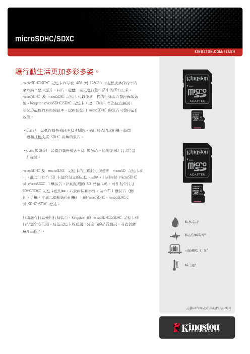
/FLASH請參閱背面之產品特性/規格 >>microSDHC/SDXC防水設計1防震與耐衝擊2耐高溫4可防機場 X 光3microSDHC/SDXC 記憶卡容量從 4GB 到 128GB ,可提供更多儲存空間來容納音樂、影片、圖片、遊戲-滿足您行動生活中的所有需求。
microSDHC 及 microSDXC 記憶卡可以使新一代的行動裝置發揮極致效能。
Kingston microSDHC/SDXC 記憶卡,以「Class 」作為速度級別,並保證最低資料傳輸速率,以確保使用 microSDHC 的裝置可發揮最佳效能。
•Class 4-最低資料傳輸速率為 4 MB/s 。
適用於入門款相機、遊戲 機和其他支援 SDHC 規格的裝置。
•Class 10 UHS-I -最低資料傳輸速率為 10 MB/s 。
適用於 HD 高畫質影 片錄製。
microSDHC 及 microSDXC 記憶卡的實際尺寸與標準 microSD 記憶卡相 同,此設計符合 SD 卡協會制定的記憶卡規格,且相容於 microSDHC 或 microSDXC 主機裝置。
搭配隨附的 SD 轉接卡時,可作為全尺寸SDHC/SDXC 記憶卡使用**。
若要確保相容性,請查看主機裝置 (例如,手機、平板電腦和數位相機) 上的 microSDHC 、microSDXC C 或 SDHC /SDXC 標誌。
無論您在何處使用行動裝置,Kingston 的 microSDHCC/SDXC 記憶卡都 值得您全心信賴。
每張記憶卡均通過百分之百的品質測試,並提供終 身產品保固。
讓行動生活更加多彩多姿。
本文件內容得隨時變更,恕不另行通知。
©2015 Kingston Technology Far East Co. Ltd (Asia Headquarters) No. 1-5, Li-Hsin Rd. 1, Science Park, Hsin Chu, Taiwan.版權所有。

Dell™ Mini 3i: 重要信息MicroSD 卡里的预装内容• Dell Mini 3i 用户手册• 中国导航地图(灵图天行者软件专用) • 灵图天行者导航系统用户手册• PC 同步软件注意:MicroSD 卡内的内容可能会由于您所在地域不同而不同。
您也可以通过 下载所有预装的内容。
备份MicroSD 卡内的预装内容1 确保您的手机是在开机状态,并且处于主菜单显示界面。
2 通过随手机提供的USB 连接线将您的手机和电脑相连。
3 此时屏幕会出现菜单选项,请选择大容量存储模式。
在电脑我的电脑目录可以看到新增可移动磁盘(X:)的显示。
X 表示电脑的磁盘号,根据您电脑配置不同,显示出不同的字母。
4 把光标移至可移动磁盘(X:),然后点击鼠标右键,选择复制。
5 然后把整个MicroSD 卡里面的内容粘贴到电脑或指定文件夹。
本文档中使用的其他商标和商品名称是指拥有这些标志和名称的实体或它们的产品。
Dell Inc. 对于自身商标和商品名称之外的其他商标和商品名称不享有任何所有权收益。
注意:您需要按照指示连接或断开和电脑的连接线以便完成安装。
3 此时屏幕会出现菜单选项,请选择大容量存储模式。
在电脑我的电脑目录可以看到新增可移动磁盘(X:)的显示。
X 表示电脑的磁盘号,根据您电脑配置不同,显示出不同的字母。
2 通过随手机提供的mini-USB 和USB 连接线将您的手机和电脑相连。
5 在ODS 目录内,双击合适的安装文件 (Windows Vista or Windows XP)。
安装PC 同步软件从您的电脑MicroSD 卡中备份文件夹安装PC 同步软件 (推荐使用)1 把PC 同步软件从MicroSD 卡中备份到您的电脑中(请参见“备份MicroSD 卡内的预装内容”)。
2 在您电脑备份目录中,打开ODS (OphoneDesktop Suite )目录。
3 在ODS 目录内,双击合适的安装文件(Windows Vista ®或Windows ® XP)。
一、SD规范介绍二、物理层规范三、SD Memory Card四、SDIO Card五、驱动编写一、SD2.0规范介绍1、版本SD spec1.0 低速度、低容量25M 2GSD spec1.1 高速度、低容量50M 2GSD spec2.0 高速度、高容量50M 32G2、SD规范包括(1) 物理层规范(2) 文件系统规范(3) SD卡安全规范(4) SD卡音频应用规范+其他相关应用规范(5) SD MC扩展规范移动设备(6) SDIO卡规范现在针对SD Memory 和SDIO两种类型的设备,所以下面内容只涉及子协议(1)、(6)。
3、符合SD2.0规范的设备SD卡MiniSD、MicroSD 1.0/1.1SDIO卡wifi 、GPSSDHC 2.0 最少支持class2SDXCCombo Card传输速度类型分为class0 旧的卡,class2 大于2MB/Sclass4 大于4MB/Sclass6 大于6MB/S二、物理层规范引脚SD模式SPI模式名称类型描述名称类型描述1 CD/DAT3 I/O/PP Card Direct/数据线[Bit3] CS I 片选(negtrue)2 CMD PP 命令/响应DI I 数据输入3 VSS S 电源地VSS S 电源地4 VDD S 电源正VDD S 电源正5 CLK I 时钟SCLK I 时钟6 VSS2 S 电源地VSS2 S 电源地7 DAT0 I/I/PP 数据线[Bit0] DO O/PP 数据输出8 DAT1 I/O/PP 数据线[Bit1] RSV9 DAT2 I/O/PP 数据线[Bit2] RSV2、总线传输模式SPI 串行传输、低速度SD 最多支持四线传输兼容MMC3 SD总线3.1 总线分为host device(1) comand 命令host to device 都是48位A、广播命令B、点对点命令(2) response 响应device to host根据内容不同分为R1、R3、R4、R7(48位)和R2(136位)初始化阶段,host给SD卡分配地址数据传输是有单块传输命令和多块传输命令,然后通过发送一个终止命令停止传输单块还是多块传输,通过host去配置命令先传msb 在lsb3.2 格式(1) 命令格式(2) 响应格式(3) 数据格式有两种(1) usual data bus 字节为单位发送(2) wide data bus 以块单位发送usual data :先发送高位,在发送低位一字节一字节发送wide data bus :整个数据块发送三、SD Memory Card1、初始化,发送命令读写卡中的寄存器发送命令完成读写、擦除等操作名称带宽描述CID 128 卡的ID号。
SD卡引脚及spi模式基本操作过程(摘自网络)对于SD卡的硬件结构,在官方的文档上有很详细的介绍,如SD卡内的存储器结构、存储单元组织方式等内容。
要实现对它的读写,最核心的是它的时序,笔者在经过了实际的测试后,使用51单片机成功实现了对SD卡的扇区读写,并对其读写速度进行了评估。
下面先来讲解SD卡的读写时序。
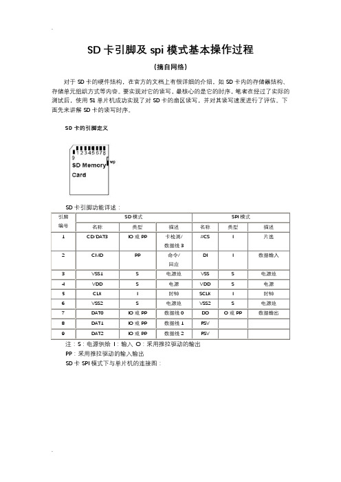
SD卡的引脚定义SD卡引脚功能详述:引脚编号SD模式SPI模式名称类型描述名称类型描述1 CD/DAT3 IO或PP 卡检测/数据线3#CS I 片选2 CMD PP 命令/回应DI I 数据输入3 VSS1 S 电源地VSS S 电源地4 VDD S 电源VDD S 电源5 CLK I 时钟SCLK I 时钟6 VSS2 S 电源地VSS2 S 电源地7 DAT0 IO或PP 数据线0 DO O或PP 数据输出8 DAT1 IO或PP 数据线1 RSV9 DAT2 IO或PP 数据线2 RSV注:S:电源供给I:输入O:采用推拉驱动的输出PP:采用推拉驱动的输入输出SD卡SPI模式下与单片机的连接图:SD卡支持两种总线方式:SD方式与SPI方式。
其中SD方式采用6线制,使用CLK、CMD、DAT0~DAT3进行数据通信。
而SPI方式采用4线制,使用CS、CLK、DataIn、DataOut进行数据通信。
SD方式时的数据传输速度与SPI方式要快,采用单片机对SD卡进行读写时一般都采用SPI模式。
采用不同的初始化方式可以使SD卡工作于SD方式或SPI 方式。
这里只对其SPI方式进行介绍。
SPI方式驱动SD卡的方法SD卡的SPI通信接口使其可以通过SPI通道进行数据读写。
从应用的角度来看,采用SPI接口的好处在于,很多单片机内部自带SPI控制器,不光给开发上带来方便,同时也见降低了开发成本。
然而,它也有不好的地方,如失去了SD卡的性能优势,要解决这一问题,就要用SD方式,因为它提供更大的总线数据带宽。
![SD2.0协议标准完整版[1-6章中文翻译]](https://img.taocdn.com/s1/m/6963f0cabb4cf7ec4afed05a.png)
mmceMMCSD-cardSPISDIO起初引⽤了⼀篇MMC相关⽂档,然⽽终究还是有些不明所以,忽觉博客不就是加⼯整理⾃⼰的思想吗,遂百度众⽂,整理归纳如下.MMC(multiMedia card)是早起记忆卡标准,于1997年由西门⼦和SanDisk推出了多媒体卡;SD卡(Secure Digital Memory Card)是⼀种基于半导体快闪记忆器的新⼀代记忆设备。
于1999年8⽉由⽇本松下、东芝及美国SanDisk公司开发研制。
SD与MMC都是存储设备的标准,包括物理硬件与协议软件,SD的软件协议与MMC的软件协议是不同的协议,物理硬件也不同。
SD相对MMC增加了数据权限功能,防⽌数据被他⼈复制,增加了安全性。
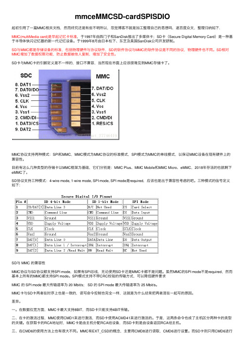
SD卡与MMC卡的引脚定义是不⼀样的,接⼝不兼容,当然现在市⾯上应该很难见到MMC存储卡了。
MMC协议⽀持两种模式:SPI和MMC,MMC模式为MMC协议的标准模式,SPI模式为MMC的单线模式,以保证MMC设备在现有硬件上的兼容性。
⽬前有这么⼏种类型的存储卡以MMC框架为基础,它们分别是:MMC Plus、MMC Mobile和MMC Micro、eMMC,2018年存活的也就剩下eMMC了。
SD协议⽀持三种模式:4-wire mode, 1-wire mode, SPI mode, SPI mode是required,应该也是出于兼容性考虑的吧。
三种模式的信号定义如下:SD与 MMC 的兼容性MMC协议与SD协议都⽀持SPI mode,如果有SPI总线,⽆论使⽤SD卡还是MMC卡都不是问题。
虽然MMC的SPI mode不是required,然⽽基本上所有的MMC都⽀持SPI mode。
SPI模式⽀持不带CRC校验的传输⽅式,可以降低硬件要求MMC 的 SPI mode 最⼤传输速率为 20 Mbit/s; SD 的 SPI mode 最⼤传输速率为 25 Mbit/s。
MMC卡与SD卡两者在时序上也是⼀致的,读写命令控制也完全⼀样,这就是为什么经常把两者混在⼀起写的原因。
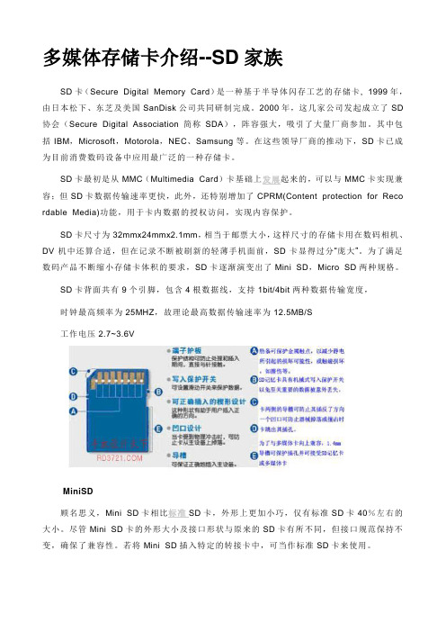
多媒体存储卡介绍--SD家族SD卡(Secure Digital Memory Card)是一种基于半导体闪存工艺的存储卡, 1999年,由日本松下、东芝及美国SanDisk公司共同研制完成。
2000年,这几家公司发起成立了SD 协会(Secure Digital Association简称SDA),阵容强大,吸引了大量厂商参加。
其中包括IBM,Microsoft,Motorola,NEC、Samsung等。
在这些领导厂商的推动下,SD卡已成为目前消费数码设备中应用最广泛的一种存储卡。
SD卡最初是从MMC(Multimedia Card)卡基础上发展起来的,可以与MMC卡实现兼容;但SD卡数据传输速率更快,此外,还特别增加了CPRM(Content protection for Reco rdable Media)功能,用于卡内数据的授权访问,实现内容保护。
SD卡尺寸为32mmx24mmx2.1mm,相当于邮票大小,这样尺寸的存储卡用在数码相机、DV机中还算合适,但在记录不断被刷新的轻薄手机面前,SD卡显得过分“庞大”。
为了满足数码产品不断缩小存储卡体积的要求,SD卡逐渐演变出了Mini SD,Micro SD两种规格。
SD卡背面共有9个引脚,包含4根数据线,支持1bit/4bit两种数据传输宽度,时钟最高频率为25MHZ,故理论最高数据传输速率为12.5MB/S工作电压2.7~3.6VMiniSD顾名思义,Mini SD卡相比标准SD卡,外形上更加小巧,仅有标准SD卡40%左右的大小。
尽管Mini SD卡的外形大小及接口形状与原来的SD卡有所不同,但接口规范保持不变,确保了兼容性。
若将Mini SD插入特定的转接卡中,可当作标准SD卡来使用。
TransFlash(Micro SD)Transflash卡,也称T-Flash卡,TF或T卡,最早由SanDisk推出。
T卡仅有11mmx 15mmx1mm大小,仅相当于标准SD卡的1/4,比Mini SD卡还要小巧。