Memory-based and disk-based algorithms for very high degree permutation groups
- 格式:pdf
- 大小:160.86 KB
- 文档页数:8


The flexibility to solve today’s tough problems...and get ready for tomorrowAgilentESA-E SeriesSpectrum AnalyzersThe Agilent ESA-E seriesFull measurement accuracy after just a five minute warm-up.Built-in tracking generator provides an RF source for scalar network analysis (optional).External mixing extends frequency range to 325 GHz. (optional)Weather resistant front panel allows operation in rain and high humidity.Built-in help function eliminates the need to carry manuals into the field.Zoom windows provides split screen display with both wide and narrow spans.Large high-resolution,high-contrast color display makes viewing multiple traces easy.Rugged case with rubber encased front and rear frames resists transportation stresses.Flexible hardware/software environment allows focused applications like GSM and cdmaOne.Built-in floppy disk drive provides PC compatibility and data archiving.Speed, accuracy, and dynamic range ...with a flexible platform for the future!2Built-in counter precisely identifies signals using the 1 Hz marker-basedcounter.A platformbuilt for speedAgilent uses the latest digital, RF and microwave designs to deliver the performance typically found in more expensive spectrum analyzers. The ESA-E series portable spectrum analyzers have a remarkableone-millisecond RF sweep timeand virtual real-time measurement updates to the display or through GPIB. Along with narrow digital resolution bandwidth filters (10 Hz to 300 Hz), and fast, time-domain sweeps you’ll spend less time testing and have your product to market faster.Specification summary*Designed for performance measurements and...• Fast test times• Superior resolution• Wide dynamic range• Measurement confidence*Includes optional performance, see ESA-E series technical specifications for complete details, literature number 5968-3386E.3 Frequency range summary*Choose the performance you need, when you need itThe Agilent ESA-E’s flexible platform means you can get exactly what you need today while still protecting your investment into the future. The six-slot option card cage lets you choose only the performance you need now (without paying for unneeded capability) and upgrade in the future.This scalable performance in com-bination with Agilent measurement personalities, downloaded into the internal memory, transform the ESA-E analyzer into an application-focused solution built around your unique needs.Built-in card cageprovides the flexibility to add application-specific performance....the flexibility to tailor that performance to your needs...Designed for upgradeabilityAfter the purchase of your analyzer,most optional performance can be installed and calibrated at an Agilent Service Center or in many cases, installed in your facility.Firmware upgrades, including many performance enhancements, are available free by download from the Agilent Web site.Over 35 options tochoose from...and more in the futureIncluding:•Digital resolution bandwidth filters of 10, 30, 100, 200 EMI, and 300 Hz •Time-gated spectrum analysis •FM demodulation/deviationmeasurements plus tune and listen •TV trigger with color picture on screen•1.5/3.0 GHz built-in tracking generator•30 Hz low frequency extension •Fast time-domain sweeps to 25 ns •Additional user memory to 10 MB •External mixing capability to 325 GHz•RF and digital demodulation/communication hardware •75 Ωinput•Snap on battery pack or 12 Vdc operation•Decreased phase noise at wide offsets for greater ACPR dynamic range•Software to perform remote spectrum analyzer control over the internetFor a complete list of options and accessories with ordering andcompatibility information please see the Agilent ESA/EMC Spectrum Analyzer Configuration Guide (literature #5968-3412E).4We’ll build one just for you.5...then add measurement personalities to create application focused solutions.Combine the ESA-E seriesoptional hardware configurations with downloadable measurement personalities to create application specific solutions.Measurement personalitiesFor a growing number of applications Agilent offers unique softwareprograms (provided on 3.5-in. disks)designed specifically for the ESA-E series. Downloaded into analyzer memory, each measurement person-ality provides measurement setups,routines,and results specific to your application, including a user interface with related terminology.Cable fault locationOptions 225 (measurement personali-ty), 1DN (tracking generator)and B7K (measurement kit) combine to identify distance to cable discontinuities for fault location and troubleshooting ofcable installation and maintenance.•Easy to use one-button measurements•Complex algorithms executed with a button press•Improved accuracy and repeatability•Operator independent results •Decreased training time •Improved productivityPhase noiseOption 226 (measurement personality)provides a log plot of phase noise in dBc/Hz versus offset frequency.Cable TV service and installationOption 227 (measurement personality)provides Cable TV operators fast,accurate and rugged spectrumanalysis for field installation, ingress evaluation and troubleshooting.General purpose measurement personalities6cdmaOneOptions BAC (measurement personality) and B74 (RF and digital demodulation hardware) combine to make the cdmaOne standard tests such as ACPR that are required to verify the perform-ance of cdmaOne transmitters.GSM/GPRSOptions BAH (measurement person-ality) and B74 (digital demodulation hardware) combine to provide all the GSM 450/900, DCS1800, PCS1900 tests required to verify the performance of GSM/GPRS mobile and BTS transmitters.Bluetooth ™Option 304 (measurement personality and digital demodulation hardware)provides one-button standard compliant Bluetooth transmitter measurements.Communication focused measurement personalities7Modulation analysisOption 229 (measurement person-ality) and B74 (RF and digitaldemodulation hardware) combine to allow measurements of EVM and related metrics for all major 2G/3G formats. Constellation and eye diagrams are provided to helpverify modulation quality.PerformancePortability8Ease-of-use9Productivity with speed,accuracy and dynamic rangeUp to 220 times faster than analogNow you don’t have to buy a high-priced spectrum analyzer to get advanced technology. The ESA-E series with its optional digital 10 Hz resolution bandwidth gives you sweep times up to 220 times faster than analog!Optional digital narrow resolution bandwidth filters (10 Hz, 30 Hz, 100 Hz,200 Hz and 300 Hz) provide the resolving power to measure closely spaced signals, plus give a narrow shape factor (≤5:1) for superior resolution. The filters deliver a lower noise floor and increased measurement sensitivity for a larger measurement range.Verify your designs with confidenceReduce project time with spectrum-analysis capabilities that optimize your designs. The ESA-E seriesoffers ±1 dB amplitude accuracy, 0.5%span accuracy,±101 Hz frequency accuracy,and a continuously phase-locked synthesizer for stability and repeatability. Calibrate out the frequency-related amplitude effects with built-in amplitude correction.The automatic background alignment offers continuous calibration toassure measurement confidence.Fewer measurement constraintsWhen a passband contains two or more signals such as CDMA or TDMA modulation, you don’t want dynamic range to limit your measurements.The ESA-E series has sensitivity down to –153 dBm, plus a third-order intercept point of +12.5 dBm (typically +16 dBm) and a second harmonic intercept point of+45 dBm to give you wide distortion free measurement range.Research and development10MeasureOne-button results with measurement personalitiesMeasure your designs easier with Agilent modulation analysis,Bluetooth ™, GSM/GPRS, cdmaOne,and phase noise measurement personalities. Execute complex algorithms with the press of a button by utilizing downloaded measurement personalities incombination with optional hardware.Expert yet easy EMI measurementsThe Agilent E7400A series of EMC analyzers takes advantage of the ESA-E series platform to provide precompliance measurements fordesign analysis.For more information see the Agilent EMC Analyzers and EMI Software brochure , literature number 5968-2516.View only the signals ofinterest with segmented sweep - paste together up to 32 discontinuous spans in to one sweep.CaptureCapture measurement results easily and quickly with IntuiLinkIntuiLink PC software provides easy transfer of ESA measurement trace data and images directly into MS Excel and Word documents for analysis, archiving, presentations, or printing. Transfer data and images over GPIB, RS232, or LAN.Save and restore analyzer states.Utilize automatic measurementtransfers by date and time. IntuiLink is included standard with GPIB and RS232 options.AnalyzeAnalyze measurement resultsAnalyze breadboard results easier with ESA instrument links supported by the Agilent EEsof Advanced Design System.Research and development11Characterize power statistics of nextgeneration digitally-modulated signals with leading test methods. Power Complementary Cumulative Distribution Function (CCDF)curves provide the peak to average data needed by 3G component designers.Six-offsets in ACPR allow convenient measurements on components subject to multi-carrier signals, (e.g. MCPAs).Every millisecond countsReal-time responseWhether you are tuning oscillators manually or performing high-volume, automatic tests on wireless products, the ESA-E series of spectrum analyzers gives a real-time response with up to 45 measurements per second. Eliminate your measurement-speed bottlenecks to help meet your production goals.This family of spectrum analyzers offers improved productivity, witha one-millisecond sweep time andas low as 25 ns in zero span.Use variable sweep points to optimize speed versus frequency resolution. Maximize speed by measuring only the frequencies of interest with segmented sweep.Unparalleled speed for manual or remote operationThe ESA-E series spectrum analyzers offer the following features to help you quickly build and test your products:•One-millisecond RF sweep time •25 ns zero span sweep time (optional)•Up to 45 measurements per second update to the display•Large 13.8-cm color VGA TFT active matrix display with wide viewing angle•Color VGA display output connector•Enhanced circuit tuning with continuous peak search•Instant printing (PCL5 printers)•Limit lines with large, colorfulpass/fail messagesMeasurements per secondESA-E series45 updates/sec. display45 updates/sec. GPIB8566B Turbo24 updates/sec. display 15 updates/sec. GPIB Swept-tuned spectrum analysis speedSetting a new standard for speed!Surpassing the GPIB speed record The ESA-E series surpasses the speed of the record-holding Agilent 8566B high-performance spectrum analyzer for moving data from the analyzerto a computer. Vastly improved sweep time and measurement update rate eliminate the GPIB data-rate bottleneck to help you more easily meet your productivity goals.• 45 measurements per second transferred to a computer•75 ms RF center frequencytuning time• Standard Commands for Programmable Instruments (SCPI) compliant• The Agilent 8590-series/ESA programming conversion guide • VXI plug&play drivers for ease of program development12Reduce test marginsThe excellent measurement accuracy reduces measurement uncertainty to allow for narrower test margins and improved yields. With an overall amplitude accuracy of ±1 dB,and a frequency accuracy of ±101 Hz plus the continuously phase-locked synthesizer, you get the performance you need to have confidence in your tests.Individual calibration certificate included standard with every analyzer.Built-in preamplifier maximizes sensitivityWhen your application calls for measurements of very low-level signals, the optional built-in preamplifier (to 3 GHz)in theESA-E series increases sensitivity.This high-gain, low-noise preamplifier lets you use wider bandwidths for even faster sweep times when searching for low-level signals.For circuit adjustments withreal-time results, the ESA-E series spectrum analyzers offers a one-millisecond sweep time and up to 45 measurement updates per second.13The ESA-E series hasdigital narrow resolution bandwidth filters and internal preamplifiers so you can identify low-level spurs.Leverage your software investmentIn the past decade, many manufactur-ers have installed Agilent 8590-series spectrum analyzers in automated production lines. If you are considering upgrading your automated stations to take advantage of the ESA-E series capabilities, Agilent can help preserve your software investment and minimize your change-over costs. An optional 8590-series programming code compatibility mode is available,which enables ESA-E series analyzers to work with more than 120 commonly used 8590-series programming commands.Calibrated field measurements in just FIVE minutes!The ESA-E series takes only 5 minutes to warm-up so technicians spend little time waiting for instrument stabilization. The automatic, internal background alignment feature gives consistently accurate results over varying temperatures. Measurement results are easily saved, printed or integrated into external tools for analysis and documentation using the standard 3.5 in floppy disk drive. The easy-to-use file manager with a time and date stamp helps to organize storage of measurement data. And, the optional rechargeable battery provides up to 1.9 hours of cordless operation.The tough ESA-E is field-rugged, yet offers uncompromising performance Snap-on battery provides freedomfrom AC power mains 14Easy,worry-free measurementsThe ESA-E series offers outstanding lab-grade performance, and protec-tion from the elements along with convenience and ease-of-use features tailored to field service.•Rubber-encased frames and the lack of vibration-prone internal adjustments improve reliability during transportation.•Snap-on rechargeable battery provides up to 1.9 hours of cordless operation (optional).•12 Vdc operation from automotive electrical systems•Rain-resistant front panel, shielded vents, and side-mounted fanprotect the instrument in adverse environments.•Vibration and shock resistance with solid state internal memory.Get accurate measurementsin every kind of field condition• Continuous automatic background alignment provides accuracy over varying temperature conditions.• Hard transit case, soft operating/carrying case or backpack provides choice of convenient transportation aids.•Flexible tilt handle optimizes line of sight whether the analyzer is viewed from the bench or ground.•Color display provides optimum readability regardless of lighting and viewing angle.•Find cable problems with the fault location measurement personality.•Troubleshoot cellular base stations with GSM and cdmaOne measurement personalities.•Make one-button RF power measurements for all the major2G/3G formats.Backpack with ESA to remote locations15Agilent ESA-E series – a whole product solution The performance of the ESA-E series spectrum analyzer isonly a small part of what you get from Agilent Technologies.Agilent strives to provide complete solutions that gobeyond our customers’ expectations. Only Agilent offersthe depth and breadth of enhancements, software,services, connectivity,accessibility and support to helpour customers reach their measurements objectives.Please contact Agilent for more information.Post-sales support• Standard three-year globalwarranty• Worldwide call center and calibrationservice center support network• One-year calibration intervals• FREE Firmware upgrades and servicenotes available from Agilent’s Web site• PC-based calibration software•Computer-based service training onCD-ROM•Flexible support options to meetyour needsThe Agilent ESA-E series ismanufactured in an ISO 9001registered facility to Agilent’sexacting standards.Training and access toinformation• Printer support matrix onAgilent’s Web site• Factory service training• Web-based support of frequentlyasked questions• Operation , programming andcalibration manuals on CD-ROM andon Agilent’s Web site• User and applications training•T echnical seminars•Cellular/PCS base stationtroubleshooting course•Calibration certificate standard•Localized operation manualsPC connectivity & software• Floppy disk drive• GPIB or RS232 interfaces• VXI plug&play drivers• IntuiLink spectrum analyzer software• EEsof Advanced Design Systemdriver (instrument link)•Programming examples on CD-ROM• SCPI (Standard Commands forProgrammable Instruments)• Custom software service• BenchLink web remote control software• 8590-series programming codecompatibility• 8590-series/ESA programmingconversion guideProduct peripherals andaccessories• Battery packs and 12 Vdc cables•Rack mounts•Operating/carrying, backpack andtransit cases•External mixers to 110 GHz•Preamplifiers to 26.5 GHz•High-impedance active probes•RF/MW limiters, adapters & cablesPre-sales services•Rentals, leasing, and financing• Application engineering andconsulting services• Application notes• Custom product modifications• Custom downloadable programs• Product literature available fromAgilent’s Web site• Demonstration units availablefor evaluation• Trade-up programs• Support at least 5 years beyondproduction life of product16Add an external VGA color monitor.12 Vdc operation from automotive batteries.Parallel port supports most HP printers (optional).Supports Agilent preselected external mixers (optional).Digital demodulation hardware for current and future communications systems (optional).Snap-on battery pack for portability (optional).Use an external frequency reference for even more accuracy.Input signal down converted to 21.4 MHz (optional).High speed GPIB interface(optional).17Ordering information ESA-E seriesAgilent E4401B Spectrum Analyzer 9 kHz to 1.5 GHz Agilent E4402B Spectrum Analyzer 9 kHz to 3.0 GHz Agilent E4404B Spectrum Analyzer 9 kHz to 6.7 GHz Agilent E4405B Spectrum Analyzer 9 kHz to 13.2 GHz Agilent E4407B Spectrum Analyzer 9 kHz to 26.5 GHzAdditional informationAgilent literatureNumber ESA-E Series Technical Specifications 5968-3386E ESA-E Series Configuration Guide 5968-3412E Spectrum Analyzer Selection Guide 5968-3413E ESA-E Series Self-Guided Demo 5968-3658E ESA Battery Pack Product Overview 5966-1851E EMI Pre-compliance Brochure5968-2516E N2717A Calibration Software Product Overview 5968-5478E GSM/GPRS Measurements Product Overview 5968-6871E cdmaOne Measurements Product Overview 5968-6869E TV Transmission Quality Measurements Flyer 5968-6874E Measuring Signals Above 26.5 GHz Flyer 5968-6873E Cable Fault Location Product Overview 5980-1915E Phase Noise Product Overview 5980-1191E Cable TV Product Overview5980-2297E Bluetooth™ Measurement Solutions Product Overview5980-2786EN Modulation Analysis Measurements Product Overview5988-2116EN IntuiLink Software Data Sheet 15980-3115EN BenchLink Web Remote Control Software Product Overview5988-2610ENFor the latest information on the Agilent ESA-E series see our Web page at: 1. For more information about IntuiLink software visit our Web site at: /find/IntuiLink1819Agilent Technologies’ Test and Measurement Support, Services, and AssistanceAgilent Technologies aims to maximize the value you receive, while minimizing your risk and problems. We strive to ensure that you get the test and measurement capabilities you paid for and obtain the support you need. Our extensive support resources and services can help you choose the right Agilent products for your applications and apply them successfully. Every instrument and system we sell has a global warranty. Support is available for at least five years beyond the production life of the product. Two concepts underlie Agilent’s overall support policy: “Our Promise” and “Your Advantage.”Our PromiseOur Promise means your Agilent test and measurement equipment will meet its advertised performance and functionality. When you are choosing new equipment, wewill help you with product information, including realistic performance specifications and practical recommendations from experienced test engineers. When you use Agilent equipment, we can verify that it works properly, help with product operation, and provide basic measurement assistance for the use of specified capabilities, at no extra cost upon request. Many self-help tools are available. Your AdvantageYour Advantage means that Agilent offersa wide range of additional expert test and measurement services, which you can purchase according to your unique technical and business needs. Solve problems efficiently and gain a competitive edge by contracting with us for calibration, extra-cost upgrades, out-of-warranty repairs, and on-site education and training,as well as design, system integration, project management, and other professional engineering services. Experienced Agilent engineers and technicians worldwide canhelp you maximize your productivity, optimize the return on investment of your Agilent instruments and systems, and obtain dependable measurement accuracy for thelife of those products.By internet, phone, or fax, get assistance with all your test and measurement needs.Online assistance:/find/assist Phone or Fax:United States:(tel)180****4844Canada:(tel)187****4414(fax) (905) 282-6495Europe:(tel) (31 20) 547 2323(fax) (31 20) 547 2390Japan:(tel) (81) 426 56 7832(fax) (81) 426 56 7840Latin America:(tel) (305) 269 7500(fax) (305) 269 7599Australia:(tel) 1 800 629 485(fax) (61 3) 9210 5947New Zealand:(tel) 0 800 738 378(fax) 64 4 495 8950Asia Pacific:(tel) (852) 3197 7777(fax) (852) 2506 9284Product specifications and descriptions in this document subject to change without notice. Copyright © 2000, 2001 Agilent Technologies Printed in USA, March 27, 20015968-3278EMicrosoft Excel® and Microsoft Word® are U.S. registered trademarks of Microsoft Corp. Bluetooth™ is a trademark owned by Telefonaktiebolaget LM Ericsson, Sweden and licensed to Agilent Technologies.。

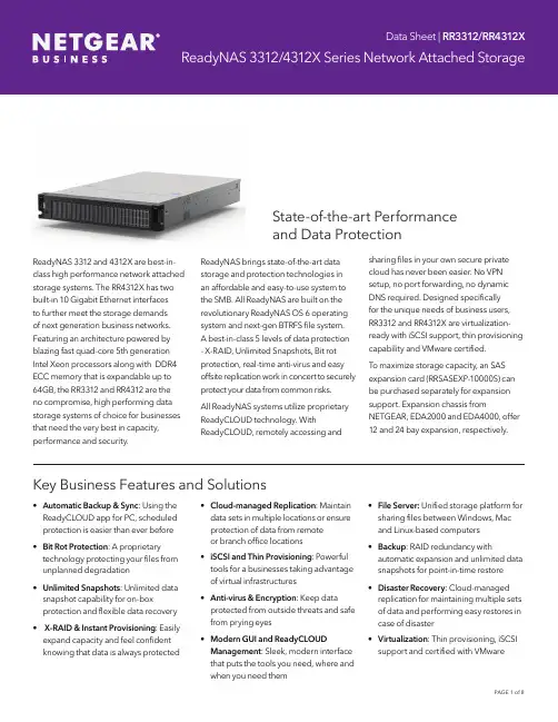
State-of-the-art Performance and Data ProtectionReadyNAS 3312 and 4312X are best-in-class high performance network attached storage systems. The RR4312X has two built-in 10 Gigabit Ethernet interfacesto further meet the storage demandsof next generation business networks. Featuring an architecture powered by blazing fast quad-core 5th generation Intel Xeon processors along with DDR4 ECC memory that is expandable up to 64GB, the RR3312 and RR4312 are the no compromise, high performing data storage systems of choice for businesses that need the very best in capacity, performance and security.ReadyNAS brings state-of-the-art datastorage and protection technologies inan affordable and easy-to-use system tothe SMB. All ReadyNAS are built on therevolutionary ReadyNAS OS 6 operatingsystem and next-gen BTRFS file system.A best-in-class 5 levels of data protection- X-RAID, Unlimited Snapshots, Bit rotprotection, real-time anti-virus and easyoffsite replication work in concert to securelyprotect your data from common risks.All ReadyNAS systems utilize proprietaryReadyCLOUD technology. WithReadyCLOUD, remotely accessing andsharing files in your own secure privatecloud has never been easier. No VPNsetup, no port forwarding, no dynamicDNS required. Designed specificallyfor the unique needs of business users,RR3312 and RR4312X are virtualization-ready with iSCSI support, thin provisioningcapability and VMware certified.To maximize storage capacity, an SASexpansion card (RRSASEXP-10000S) canbe purchased separately for expansionsupport. Expansion chassis fromNETGEAR, EDA2000 and EDA4000, offer12 and 24 bay expansion, respectively.Key Business Features and Solutions• Automatic Backup & Sync: Using the ReadyCLOUD app for PC, scheduled protection is easier than ever before• Bit Rot Protection: A proprietary technology protecting your files from unplanned degradation• Unlimited Snapshots: Unlimited data snapshot capability for on-box protection and flexible data recovery • X-RAID & Instant Provisioning: Easily expand capacity and feel confident knowing that data is always protected • Cloud-managed Replication: Maintaindata sets in multiple locations or ensureprotection of data from remoteor branch office locations• iSCSI and Thin Provisioning: Powerfultools for a businesses taking advantageof virtual infrastructures• Anti-virus & Encryption: Keep dataprotected from outside threats and safefrom prying eyes• Modern GUI and ReadyCLOUDManagement: Sleek, modern interfacethat puts the tools you need, where andwhen you need them• File Server: Unified storage platform forsharing files between Windows, Macand Linux-based computers• Backup: RAID redundancy withautomatic expansion and unlimited datasnapshots for point-in-time restore• Disaster Recovery: Cloud-managedreplication for maintaining multiple setsof data and performing easy restores incase of disaster• Virtualization: Thin provisioning, iSCSIsupport and certified with VMwareHardware ReadyNAS 3312ReadyNAS 4312S ReadyNAS 4312XCPU-10000S Intel Xeon E3-1225v63.3GHzQuad Core Processor,Max Turbo Speed3.7GHzIntel® Xeon E3-1245v6 3.5GHzQuad Core, HyperThreaded Processor,Max Turbo Speed3.9GHzIntel® Xeon E3-1245v6 3.5GHzQuad Core, HyperThreaded Processor,Max Turbo Speed3.9GHzCPU-20000S Intel Xeon E3-1225v63.3GHz, Max TurboSpeed 3.7GHzIntel Xeon E3-1245v63.5GHz, Max TurboSpeed 3.9GHzIntel Xeon E3-1245v63.5GHz, Max TurboSpeed 3.9GHzMemory8GB DDR4 ECC16GB DDR4 ECC16GB DDR4 ECC Memory Expansion64GB DDR464GB DDR464GB DDR4 Drive Bays121212Drive T ypes Supported SATA/SSD 2.5” or 3.5”SATA/SSD 2.5” or 3.5”SATA/SSD 2.5” or 3.5”Hot Swappable Drives Yes Yes Yes eSATA Ports222SAS Ports for Expansion Chassis (sold separately)222 Gigabit LAN Ports44410Gbps LAN Optical SFP+02010Gbps LAN Copper 10GBase-T002USB Ports2x USB3.02x USB3.02x USB3.0Power SupplyDual RedundantInternal 550 W; input100-240V AC,50-60HzDual RedundantInternal 550 W; input100-240V AC,50-60HzDual RedundantInternal 550 W; input100-240V AC,50-60HzChassis Warranty5 years including5 years NextBusiness Day hard-ware replacement5 years including5 years NextBusiness Day hard-ware replacement5 years including5 years NextBusiness Day hard-ware replacementFan (mm) 3 x 80 3 x 80 3 x 80 Dimensions DxWxH (mm)707 x 445 x 88 707 x 445 x 88 707 x 445 x 88 Weight (diskless) (kg)11.96 11.96 11.96 Software and Functionality ReadyNAS 3312ReadyNAS 4312S ReadyNAS 4312XCertification and Compatibility VMware vSphereESXi 6.0 VMware vSphereESXi 6.0VMware vSphereESXi 6.0Cloud-discovery, Setup and Management Yes Yes Yes Data Protection with Unlimited Snapshots Yes Yes Yes Web-managed Replication for Disaster Recovery Yes Yes Yes Real-time Antivirus Yes Yes Yes iSCSI and Thin Provisioning Yes Yes Yes ReadyNAS Rackmount ComparisonTechnical SpecificationsData Protection (Backup & Replication)• Unlimited block-based snapshots for continuous data protection• Restore Snapshots to any point in time• Restore Snapshot data from local admin GUI, ReadyCLOUD, or native Windows File Explorer• Scheduled and manual snapshots• File Synchronization (rsync)• Encrypted Remote Replication• Data compression• Cloud managed Remote Replication (ReadyNAS to ReadyNAS). No licenses required for ReadyNAS OS 6 devices.• AES 256-bit volume based encryption• X-RAID (automatic single volume online expansion)• Single Disk, JBOD• RAID Levels: 0, 1, 5, 6, 10, 50, 60• RAID Global Hot Spare• Backup to external storage (USB/eSATA)• Apple Time Machine support• Amazon Cloud Drive synchronization (requires Amazon account)• ReadyNAS Vault™ Cloud backup (optional service)• Dropbox™ file synchronization (requires Dropbox account)• Real-time Anti-Virus scanning using signature and heuristic algorithms. (No end-user licenses required)Protection for viruses, malware, worms, and Trojans.• Bitrot automatic detection & correction for degraded mediaStorage Area Networks (SAN), Virtualization• Unlimited iSCSI LUN Snapshot• Thin or thick provision LUNs• Multi-LUN per target• LUN mapping and masking• SPC-3 Persistent Reservation (iSCSI)• MPIO and MC/S (iSCSI)• Max # iSCSI Target: 256• Max # iSCSI LUN: 256• VMware vSphere 6• Citrix XenServer 6• Windows Server 2008 Hyper-V• Windows Server 2008 Failover Clustering• Windows Server 2012 R2ReadyCLOUD (cloud access to ReadyNAS• ReadyCLOUD portal based data access and management• Upgrade firmware remotely• VPN quality remote data transfer and management• Share data with friends & co-workers directly from portal• Share file via email linkReadyCLOUD Client Applications• ReadyCLOUD client applications for Apple OS X, Microsoft Windows, Android, and Apple iOS• VPN quality remote data transfer and management• Simple remote access through ReadyCLOUD client (no firewall or router configuration needed)• Sync files/folders between PC (Mac/Windows) & ReadyNAS• Sync files/folders between multiple PCs and ReadyNAS• Sync files/folders between multiple users and ReadyNAS• Backup files/folders from PC to ReadyNASFile System & Transfer Protocols• ReadyNAS OS 6.5 or later• Linux 4.x• Internal File System: BTRFS• External File System: EXT3, EXT4, NTFS, FAT32, HFS+• Copy-on-write file system• Microsoft Network (CIFS/SMB 3)• Apple OS X (AFP 3.3)• Linux/Unix (NFS v4)• Internet (HTTP)• Secure Internet (HTTPS)• File Transfer Protocol (FTP)• FTP over SSL / TLS (explicit)• FTP Passive mode with port range setup• FTP Bandwidth control• FTP Anonymous• FTP Transfer Log• Secure Shell (SSH)• Web Authoring (WebDAV)• Storage Array Network (iSCSI)• File Synchronization (rsync)• Local web file managerUsers/Groups• Max # Users: 8192• Max # User Groups: 8192• Max # Share Folder: 1024• Max # Concurrent Connections: 1024• Share Folder Level ACL Support• Advanced Folder Permissions with Subfolder ACL support for CIFS/SMB, AFP, FTP• Microsoft Active Directory (AD) Domain Controller Authentication• Local access list• ReadyCLOUD based ACL• Domain user login via CIFS/SMB, AFP, FTPManagement• ReadyCLOUD cloud based discovery and management• RAIDar local discovery agent (Windows/Mac)• Save and restore system configuration (clone devices)• Local event log• Local Graphical User Interface (GUI) Languages: English, German, French, Japanese, Chinese (Traditional &Simplified), Russian, Swedish, Portuguese, Italian, Spanish, Polish, Czech, Dutch, Korean• Unicode support• Volume Management• Thin provision Shares and LUNs• Instant Provisioning/Expansion with data protection• Restore to factory default• Operating Systems supported: Microsoft Windows 7, 8/8.1, 10, Microsoft Windows Server 2008 R2/2012, AppleOS X, Linux/Unix, Solaris, Apple iOS, Google Android• Supported Web Browsers (Microsoft Internet Explorer 9+, Microsoft Edge, Mozilla Firefox 14+, Google Chrome50+, Apple Safari 5+)System Monitoring• Device capacity, performance, resource and health monitoring• Bad block scan• Hard Drive S.M.A.R.T.• File System Check• Disk Scrubbing• Disk Defragment• Volume balance• Alerts (SMTP email, SNMP, local log)• Auto-shutdown (hard drive, fan, UPS)• Auto-restart on power recoveryNetworking Protocols• TCP/IP• IPv4• IPv6• Static IP Address• Dynamic IP Address• Multiple IP Settings• DHCP Client• UPnP Discovery• Bonjour Discovery• Link Aggregation IEEE 802.3ad• Port Trunking (balanced round robin, active backup, balance xor, broadcast, 802.3ad link aggregation LACP,transmit load balancing, adaptive load balancing)• Hash Types IEEE 802.3ad LACP or XOR (Layer 2, Layer3, Layer 4)• Jumbo Frames• Static routes• Secure Shell (SSH)• Simple Network Management Protocol v2, v3• Network Time Protocol (NTPMedia• ReadyDLNA (UPnP DLNA Media Server)• ReadyDLNA streams to any compliant device including Playstation and Xbox• ReadyDLNA mobile clients for remote media streaming (iOS, Android)• ReadyDLNA supported music formats (wav, wma, pcm, ogg, mp3, m4a, flac, aac)• ReadyDLNA supported photo formats (jpg, jpeg)• ReadyDLNA supported video formats (3gp, mp4, wmv, xvid, vob, ts, tivo, mts, mpeg, mpg, mp4, mov, mkv, m4v,m4p, m2t, m2ts, flv, flc, fla, divx, avi, asf)• ReadyDLNA supported playlist formats (pls, m3u)• ReadyNAS Surveillance (free trial, license required) supports over 70 brands and 1600 models of IP cameras• iTunes Server• iTunes supported audio formats (mp3, m4a, m4p, wav, aif)• iTunes supported video formats (m4v, mov, mp4)• iTunes supported playlist formats (m3u, wpl)• TiVo Archiving• Plex Media Server streams to DLNA and Plex clients (mobile, desktop, Android TV, Roku, Samsung & LG TVs)HardwareCPU• ReadyNAS 3312: Intel® Xeon E3-1225v5 3.3GHz Quad Core Processor, Max Turbo Speed 3.7GHz• ReadyNAS 4312S: Intel® Xeon E3-1245v5 3.5GHz Quad Core, Hyper Threaded Processor, Max Turbo Speed 3.9GHz• ReadyNAS 4312X: Intel® Xeon E3-1245v5 3.5GHz Quad Core, Hyper Threaded Processor, Max Turbo Speed 3.9GHzMemory• ReadyNAS 3312: 8GB DDR4 ECC• ReadyNAS 4312S:16GB DDR4 ECC• ReadyNAS 4312X:16GB DDR4 ECC• Memory Expansion: 64GB DDR4• Flash: 256MB for OS• 12 Hot Swappable Drive Bays• Drive Types Supported: SATA/SSD 2.5” or 3.5”• Two eSATA ports• Two USB3.0 ports• Total solution capacity: 120TB w/o expansion 600TB w/ 2 x EDA4000• RR4312X: dual 10GbE copper ports• RR4312S: dual 10GbE SFP+ ports• Quad Gigabit Ethernet ports with link aggregation and failover• LEDs: Power, System, 4 x LAN• Three 80mm fans• Dimensions (DxWxH):707mm x 445mm x 88mm• Weight (diskless): 11.96 kg• Dual 550 watt redundant power supplies• Power cord localized to country of sale• Rackmount sliding rail includedCompliance• ENGR 10049 EST Environmental Stress Test Guideline• ENGR 10045 EVT Engineering Validation Test Guideline• ENGR 10048 CVT Compliance Validation Test Guideline• ENGR 10046 System Validation Test Guideline• ENGR 10023 HALT Accelerated Life Test Guideline• ENGR 10036 CDG Component Derating GuidelineEnvironment• Noise levels: <49dBA @ 25C• Operating Temperature: 0-45C• Operating Humidity: 20-80% relative humidity, non-condensing• Smart Fan• Scheduled Power on/off• UPS Support• Network UPS with SNMP Management• Wake on LANEnvironment• Hard drive disk spin down• Auto-power on (after shutdown)• AC Input Power Voltage 100V to 240V• Power Frequency: 50Hz to 60Hz, Single Phase• Power Consumption (Max/Wake on LAN) RR3312: 210/9.2 watts• Power Consumption (Max/Wake on LAN) RR4312S: 210/9.2 watts• Power Consumption (Max/Wake on LAN) RR4312X: 210/9.2 watts• Certification: FCC Class A, CE Class A, RoHS, VCCI Class A• MTBF: 70,723 hoursAccessories• RTRAY04-10000S: Replacement/additional 3.5” or 2.5” hard drive tray• RFAN04-10000S: Replacement 80mm fan• RRAIL03-10000S: Replacement/additional sliding rack mount rail• RPSU03-10000S: Replacement/additional 550W power supply unit• RMEM04-10000S: Replacement 8GB memory module for RR3312 and RR4312X• RMEM05-10000S:16GByte DDR4 ECC U-DIMM 2Rx8 Memory Expansion, applicable to RR3312, RR4312X andRR4312S• RRSASEXP-10000S: SAS Expansion cardAdd-on Applications• One click installation of add-on applications directly through local GUI• Application available for productivity, media, backup, surveillance, and many others• NETGEAR applications include Surveillance, Photo Sharing, Advanced configuration tools• Partner applications include BitTorrent Sync, Plex, Memeo, DVBlink• Community applications include Transmission, ownCloud, qBittorent, MySQL, VPN server, Syslog, Wordpress,joomla, Media Wiki, and others• Application availability subject to change• Applications may impact overall performance• Software Development Kit (SDK) available for 3rd party developersWarranty and SupportHardware Limited Warranty 5 years*Next-Business-Day (NBD) Replacement YesT echnical Support 90 days free from date of purchase** This product comes with a limited warranty that is valid only if purchased from a NETGEAR authorized reseller, and covers unmodified hardware, fans and internal power supplies – not software or external power supplies, and requires product registration at https:// or using the Insight App within 90 days of purchase; see https:///about/warranty for details. Intended for indoor use only.NETGEAR, the NETGEAR Logo, ReadyNAS, ReadyCLOUD, ReadyNAS Vault, and X-RAID are trademarks of NETGEAR, Inc. in the United States and/or other countries. Other brand names mentioned herein are for identification purposes only and may be trademarks of their respective holder(s). Information is subject to change without notice.© 2022 NETGEAR, Inc. All rights reserved.NETGEAR,Inc.350E.PlumeriaDrive,SanJose,CA95134-1911USA,1-888-NETGEAR(638-4327),E-mail:****************,DS-3312/4312S/4312X -25May22。


Disulfide by Design Version 1.20© Wayne State University 2003, All Rights Reserved09/16/03Users’ GuideAlan A. Dombkowski, Ph.D., Institute of Environmental Health Sciences,Wayne State University, Detroit, MI domski@Contents1 Description (2)Requirements (2)2 System3 Installation (2)4 Running Disulfide by Design (2)4.1 Loading a PDB file (3)4.2 Run (4)4.3 Output (4)4.4 SavingResults (4)4.5 Creating a mutant PDB file (5)5 Options (5)Intra-chain (5)and5.1 InterCβ for glycines (5)5.2 Building5.3 Chi3 torsion angle tolerance (5)5.4 Ca-Cb-S angle tolerance (6)Details (6)6 TechnicalNotes (7)7 Release8 References (7)1 DescriptionDisulfide by Design is an application for the rational design of disulfide bonds in proteins. For a given protein structural model, all residue pairs are rapidly assessed for proximity and geometry consistent with disulfide formation, assuming the residues were mutated to cysteines. The output displays residue pairs meeting the appropriate criteria. The input model will typically be a Protein Data Bank (PDB) structure for the protein of interest; however, structures developed through homology modeling may also be used. Engineered disulfides have proven useful for increasing the stability of proteins and to assist the investigation of protein dynamics and interactions. This software was written by Dr. Alan Dombkowski and based on algorithms created for disulfide identification in protein fold recognition methods (Dombkowski & Crippen, 2000). The Disulfide by Design algorithm has been successfully used for disulfide engineering (Anthony et al., 2002; Anthony & Burgess, 2002).2 System RequirementsDisulfide by Design is currently available for the Windows operating system. It has been tested with Windows 98, NT, 2000 and XP. The application uses about five megabytes of memory and less than one megabyte of disk space. Monitor resolution should be a minimum of 1024 x 768 with 16 or 32 bit color.3 InstallationSimply double click on “Disulfide by Design Install.exe” and the installer will step you through the installation process. A license agreement will be displayed during the installation process. Proceeding with installation requires agreement with the software license. Upon installation, an icon will be installed under the “Programs” tab of the “Start” menu. To run the program simply double-click the icon. The software can be uninstalled using the Add/Remove Programs tab of the control panel.4 Running Disulfide by DesignRunning Disulfide by Design is as simple as loading a PDB file then pressing “Run.” The default option settings are recommended for general use. However, it may be desirable to change option settings, such as to increase assessment criteria stringency. The options are discussed in greater detail below.4.1 Loading a PDB fileThe input file must be in PDB format with atomic coordinates. File selection isperformed with the “Load Structure” button. All residues with a complete main chainbackbone and a Cβ atom are used in the analysis. In the case of glycine, a Cβ will becreated if the “Build Cb for Gly” check box is selected. After the structure file has beenread a message is displayed showing the number of residues having a complete backbone and Cβ. For NMR structures with multiple models only the first model will be used.124.2 RunAfter successful loading of a PDB file, simply press “Run” to start the analysis. Each possible pair of residues will be assessed for potential disulfide formation, assuming the residues were mutated to cysteines. With the default setting, both inter and intra-chain disulfides are analyzed. Deselect the appropriate check box to change the intra/inter-chain setting.4.3 OutputThe output text box displays one line per potential disulfide. Each line shows a pair of residues that have the appropriate geometry to form a disulfide bond if the residues were mutated to cysteines. The analysis is based on the assumption that the mutations would not significantly perturb the protein backbone conformation. Each displayed disulfide meets the minimum geometric criteria, including user-selected parameters. The chain id, residue number, and original amino acid type are shown for each residue in the pair. Chain id and residue number are consistent with the input PDB designations. Also shown are the estimated χ3 torsion angle and an energy value in kcal/mol. χ3 angles of known disulfides have a bimodal distribution with peaks observed at +100 and -80 (Petersen et al., 1999), see figure in technical details. These values provide useful selection criteria for disulfide design. The estimated chirality and torsion angle are based on the best possible orientation of putative mutant cysteine Sγ atoms, as determined by an energy minimization performed within Disulfide by Design (see technical details below). The energy value is useful for comparison of potential disulfides to select the best possible candidates. Disulfides with a lower energy value are preferential to those with a higher score. The calculated energy is not intended as a comprehensive assessment of conformational energy, but it is provided to allow comparisons of prospective disulfide bonds. Figure 3 is a histogram of energy values calculated for 706 known disulfides using the Disulfide by Design algorithm. This data reveals the distribution of energy values for naturally occurring disulfides and may be helpful when selecting putative bonds for disulfide engineering. The mean energy value is 1.07 kcal/mol and the maximum observed value is 7.91 kcal/mol.4.4 Saving ResultsResults displayed in the output text box can be saved to a user-specified file using the “Save Results” button. Text is saved in tab-delimited format, so the data can easily be imported into Excel or other spreadsheet software.4.5 Creating a mutant PDB fileA modified form of the original input PDB file can be created by selecting one or more of the potential disulfides then pressing “Create PDB File.” Disulfides are selected by simply pointing the mouse at the desired line then left-clicking. Disulfides may be deselected by clicking a second time. For each disulfide selected, the original amino acids are replaced in the PDB file with cysteines. The respective SSBOND records are inserted near the beginning of the mutant PDB file. The mutant PDB file can be subsequently imported into molecular modeling software such as Rasmol for visualization of the designed disulfides.5 Options5.1 Inter and Intra-chainBy default, Disulfide by Design checks all potential inter and intra-chain disulfides. However, it may be desirable to restrict analysis to either inter or intra-chain. This is accomplished by simply deselecting the appropriate check box.5.2 Building Cβ for glycinesThe disulfide design algorithm requires coordinates for Cβ atoms to determine the potential for disulfide formation. Since glycine residues do not include a Cβ atom they cannot be used in the analysis unless a Cβ is created. The “Build Cb for Gly” check box enables the construction of Cβ atoms. The Cβ location is determined by using the coordinates of the residue backbone atoms. The algorithm was tested by building Cβatoms for cysteine residues of proteins with a known structure. The coordinates of the constructed atoms were compared with the actual Cβ locations, and the average distance was only 0.12 Å indicating accurate modeling of the Cβ atoms.5.3 Chi3 torsion angle toleranceThe χ3 torsion angle is formed by the Cβ-Sγ-Sγ-Cβ bonds, with rotation about the Sγ-Sγbond (see Figure 1 below). The distribution of χ3 angles observed in disulfides of known protein structures is bimodal with sharp peaks at +100 and -80 (see Figure 2 below). It may be desirable to restrict candidate disulfides to those having an estimated χ3 value that falls within the region of observed χ3 values. The χ3 angle tolerance can be selected in the options box. The default setting is +100 ± 30º and -80 ± 30º. If numerous putative disulfides are identified using the default setting it may be useful to decrease the tolerance resulting in a shorter list with preferential characteristics.5.4 Ca-Cb-S angle toleranceThe distribution of C α−C β−S γ angles observed in known disulfides has a peak near 115º and covers a range from approximately 105º to 125º (Petersen et al., 1999). The tolerance of this bond angle is selectable, with a default setting of 114.6 ± 10º.6 Technical DetailsFigure (1) represents a cysteine pair coupled by a disulfide bond. The approach uses a disulfide model with fixed C β-S γ and S γ-S γ bond lengths, 1.81 and 2.04 Å respectively, and fixed C β-S γ-S γ bond angles of 104.15º. These bond lengths and angles are consistent with values observed in a survey of protein disulfide bonds (Petersen et al ., 1999). The χ3 torsion angle, formed by rotation of the C β atoms about the S γ-S γ bond, is allowed to vary in the model and can be described as a function of the distance between C β atoms(Dombkowski & Crippen, 2000). To “fit” the disulfide model between a pair of residues, the algorithm simply rotates the χ3 angle to obtain a C β-C β distance that matches the C β-C β distance measured between the residues. Numerous S γ locations are possible, so all possible S γ orientations are examined and the atomic coordinates providing the lowest energy (E ij ) are selected, based on the χ1 and χ3 torsion angles and the two C α-C β-S γ angles. The χ1 torsion angle is defined by the N-C α-C β-S γ atoms . E ij is calculated per equations (1-4), where i and j are residue indices, θ is the C α-C β-S γ angle, and θ0 is set to 114.6º. Energy units are kcal/mol.)()()()()(3,1,1j i j i ij E E E E E E θθχχχ++++=(1)[])3cos(14.1)(11χχ+=E (2)[])1602cos(10.4)(33+−=χχE (3)[]200.55)(θθθ−=E (4)The energy calculation provides minima at χ3 values of +100º and -80º and χ1 values of ±60º and ±180º, consistent with values observed in the latest survey of disulfide bonds (Petersen et al ., 1999). Since the disulfide model uses fixed bond lengths, no term is included for bond stretching. The energy calculation provides a means to compare potential disulfides during disulfide design. The distribution of energy values for 706 known disulfide bonds reveals a mean energy value, calculated per equations (1-4), of 1.07 kcal/mol and a maximum of 7.91 kcal/mol.7 Release NotesChanges in version 1.20 include:•Corrected bug that caused text to go beyond the right-hand border of the dialog box with some terminal settings.Changes in version 1.12 include:•Energy units are now in kcal/mol.•For residues with multiple conformers only the first set of coordinates encountered are used.•For NMR structures with multiple models only the first model found in the PDB file is used.•Fixed bug in torsion angle calculation that caused crashes for a small number of PDB structures.8 ReferencesDombkowski A.A., 2003, Disulfide by Design: A computational method for the rational design of disulfide bonds in proteins, Bioinformatics, vol. 19 no. 14, 22 Sep.2003.Anthony, L.C. and Burgess, R.R., 2002, Conformational Flexibility in sigma 70 Region 2 during Transcription Initiation, J Biol Chem. Nov 29;277(48):46433-46441.Anthony, L.C., Dombkowski, A.A., and Burgess, R.R., 2002, Using disulfide engineering to study conformational changes in the β’260-309 coiled-coil region of E. Coli RNA polymerase during σ70 binding, J Bacteriol. May;184(10):2634-41.Dombkowski A.A.and Crippen G.M., 2000, Disulfide recognition in an optimized threading potential, Protein Engineering, vol. 13 no. 10, 679-689.Petersen, M., Jonson, P.H., and Petersen, S.B., 1999, Amino acid neighbours and detailed conformational analysis of cysteines in proteins, Protein Engineering, vol. 12, no 7, 535-548.-80+100 Figure 2。
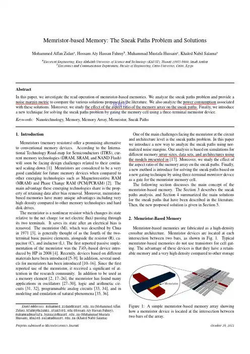
Memristor-based Memory:The Sneak Paths Problem and Solutions Mohammed Affan Zidan a,Hossam Aly Hassan Fahmy b,Muhammad Mustafa Hussain a,Khaled Nabil Salama aa Electrical Engineering,King Abdullah University of Science and Technology(KAUST),Thuwal23955-6900,Saudi Arabiab Electronics and Communication Department,Faculty of Engineering,Cairo University,Cairo,EgyptAbstractIn this paper,we investigate the read operation of memristor-based memories.We analyze the sneak paths problem and provide a noise margin metric to compare the various solutions proposed in the literature.We also analyze the power consumption associated with these solutions.Moreover,we study the effect of the aspect ratio of the memory array on the sneak paths.Finally,we introduce a new technique for solving the sneak paths problem by gating the memory cell using a three-terminal memistor device. Keywords:Nanotechnology,Memory,Memory Array,Memristor,Sneak Paths1.IntroductionMemristors(memory resistors)offer a promising alternative to conventional memory devices.According to the Interna-tional Technology Road-map for Semiconductors(ITRS),cur-rent memory technologies(DRAM,SRAM,and NAND Flash) will soon be facing design challenges related to their contin-ued scaling-down[1].Memristors are considered to be a very good candidate for future memory devices when compared to other emerging technologies such as Magnetoresistive RAM (MRAM)and Phase Change RAM(PCM/PCRAM)[2].The main advantage these emerging technologies share is the prop-erty of retaining data after bias removal.Moreover,memristor-based memories have many unique advantages including very high density compared to other memory technologies and hard disk drives.The memristor is a nonlinear resistor which changes its state relative to the net charge(or net electricflux)passing through its two terminals.It saves its state after an electrical bias is removed.The memristor(M),which was described by Chua in1971[3],is generally thought of as the fourth of the two-terminal basic passive elements,alongside the resistor(R),ca-pacitor(C),and inductor(L).Thefirst reported passive imple-mentation of the memristor was the TiO2-based device intro-duced by HP in2008[4].Recently,devices based on different materials have been introduced[5–9].In addition,several mod-els for memristors has been introduced[10–16].Since thefirst reported use of the memristor,it received a significant of at-tention in the research community.In addition to be used as a memory element[2,17–26],the memristor has found many applications in oscillators[27–30],logic and arithmetic cir-cuits[31,32],programmable analog circuits[33,34],and in modeling and emulation of natural phenomena[35,36].Email addresses:mohammed.zidan@.sa(Mohammed Affan Zidan),hfahmy@(Hossam Aly Hassan Fahmy), muhammadmustafa.hussain@.sa(Muhammad Mustafa Hussain),khaled.salama@.sa(Khaled Nabil Salama)One of the main challenges facing the memristor at the circuit and architecture level is the sneak paths problem.In this paper we introduce a new way to analyze the sneak paths using nor-malized noise margins.Our analysis is based on simulations for different memory array sizes,data sets,and architectures using the models presented in[17].Moreover,we study the effect of the aspect ratio of the memory array on the sneak paths.Finally, a new method is introduce for solving the sneak paths based on a new gating technique by using three-terminal memistor device as a gate for the memristor memory cell.The following section discusses the main concept of the memristor-based memory.The Section3describes the sneak paths analysis,and Section4summarized the main solutions for the sneak paths that have been described in the literature. Then,the new proposed solution is given in Section5.2.Memristor-Based MemoryMemristor-based memories are fabricated as a high-density crossbar architecture.Memristor devices are located at each intersection between two bars,as shown in Fig.1.Typical memristor-based memories do not use transistors for cell gat-ing.The advantage of these devices is that they have a retain-able memory and a very high density compared to otherstorage Figure1:A simple memristor-based memory array showing how a memristor device is located at the intersection between two bars of the array.纵横比Table1:Detailed comparison between memristor-based memory,traditional memories,and other emerging memories according to the2011ITRS report[1].The abbreviations used are:T–transistor,C–capacitor,R–resistor,and D–diode.The bold font indicates the best value per row.Traditional Memories Other Emerging Technologies Redox DRAM SRAM NOR Flash NAND Flash FeRAM MRAM PCRAM Including Memristor Cell Element1T1C6T1T1T1T1C1(2)T1R1T(D)1R(1D)(1T)1R Feature Size(nm)36-6545902218065459 Density(Gbit/cm2)0.8-130.4 1.2520.14 1.212154-309 Read Time(ns)2-100.215100453512<50 Write Time(ns)2-100.210710665351000.3 Retention Time4-64ms N/A10years10years10years>10years>10years>10yearssystems.Table1shows a detailed comparison between memristor-based memory,traditional memories,and other emerging mem-ories.The memristor memory is4x as dense as the hard disk drive(HDD)[37],and23x as dense as DRAM.As a result, memristor-based memories are a good candidate for replacing both the permanent and running storages,therefore approaching the ideal model of having oneflat memory instead of memory hierarchy.The current reading and writing speeds are slower than DRAM and SRAM,but are very fast compared toflash memories,as shown in Table1.These numbers show that mem-ristors could easily replaceflash memories,while further speed enhancement is required for replacing CMOS memories.HP Labs are currently reporting a fast switching time of less than 2ns[38].Recently,Elpida Memory Inc.,reported the develop-ment of a high-speed non-volatile resistance memory[39].It is to be noted that any resistor with a hysteresis curve is consid-ered a memristor[40].HP Labs expects to come up with their memristor-based memory chip replacingflash and solid-state drives(SSD)in2013[41].2.1.Writing OperationData are stored in the memristor in the form of its resistance value,where each of the limiting resistances R o f f and R on are assigned to the two Boolean values‘0’and‘1’.R o f f and R on are the maximum and minimum resistances of the device,respec-tively.Writing one of these values is simply done by passing current through the cell of interest until the memristor’s resis-tance saturates.The saturation value(R on or R o f f)depends on the direction of the writing current.Even this simple writing operation could consume considerable of energy,depending on the values of the memristor’s resistances.2.2.Reading OperationWhile writing to the memristor is a straightforward opera-tion,reading is more challenging.In the memristor memory array,we are trying to sense a cell resistance merged in a com-plete resistive structure.This could be compared to the problem offinding a needle in a haystack.Moreover,the reading oper-ation itself could be destructive to the cell data,depending onthe device properties.2.3.Multilevel MemoryMultilevel memory is one promising application for the memristor ing such a technique would enormously increase the density of memristor-based memory,but wouldalso reduce the noise margin significantly.The current pro-posed techniques for building binary memristor-based memorysuffer from many problems that could be fatal for the multi-level memory.Some researchers believe1M is insufficient forbuilding multilevel memory,and that1M1T(one memristor andone transistor)or1M1D(one memristor and one diode)areneeded[42].We believe that addressing the current challengesfacing the binary memristor-based memory will directly solvethe multilevel memory problems.3.Sneak Paths AnalysisSneak paths are undesired paths for current,parallel to the intended path.The source of the sneak paths is the fact thatthe crossbar architecture is based on the memristor as the only memory element,without gating.Fig.2a shows an array witha simple voltage divider and its equivalent circuit.Thefigureshows the ideal case in which the currentflows from the sourceto the ground passing through only the desired cell at the inter-section between the activated column and row.Unfortunatelythis is not the real case as shown in Fig.2b.The currentflowsthrough many sneak paths beside the desired one.These pathsact as an unknown parallel resistance to the desired cell resis-tance as shown in Fig.2b.What makes the sneak paths problemharder to solve is the fact that the paths depend on the contentof the memory.This is due to the fact that the current will sneakwith more intensity through the paths with smaller resistance,which is memory content dependent.The added resistance of the sneak paths significantly narrowsthe noise margin and reduces the maximum possible size of a memristor array.To study the effect of the sneak paths on thenoise margin,we simulate memristor-based memory arrays of漏电流路径更趋向于电阻小的通路,所以漏电流依赖于存储的内容V (a)R M R SP(b)Figure 2:The reading current path through a memristor memory array and the equivalent circuit for (a)the ideal case where the current flows only through the target cell and (b)an example of a real case where current sneaks through di fferent undesired paths.The green lines show the desired path and the red ones show the e ffective sneak paths.di fferent sizes and with di fferent data sets.The sets are selected to reflect both the worst and best cases for the memory content.The worst case for the sneak paths is a memory full of “ones”since the e ffect of the sneak paths becomes more dominant as their resistance decreases.On the other hand the “all zeros”case is the best case condition since all the sneak paths are made of R o f f resistances in series.In addition tothe previouscases,checkered casestypical of real data and interleaved rows (or columns)are also used.These cases are considered as normal test cases since ones and zeros are present in equal numbers and are uniformly distributed.The simulation result is independent of the location of the cell in the array if we neglect the rows’and columns’pad resistances.We can interpret the array as a complete sphere,since connecting the terminals of each row or column will not introduce any change to the equivalent circuit as shown in Fig.3.Hence all the cell locations are equivalent from the sneak paths point of view.All the simulations werewhere a and k x are constants.The reported feasible values in [17]for the constants are a =3−1and k on =10−8A and k o f f =10−11A for the ON and OFF states of the device respec-tively.In conventional CMOS circuits,there are two regions defined for accepted values of ONEs and ZEROs [43],as shown in Fig.4.For typical CMOS circuits,the prefect ONE has the value of V OH =V dd and the perfect ZERO is V OL =GND .However,the circuit can tolerate shift in values of the input of the value detected for ONE or ZERO noise.For a given ence between voltages values representing ONE and ZERO at the target cell is a perfect measure for the sneak-path e ffect.We define a total noise margin as the region between the ON (2)the such V ol cir-and 忆阻器的位置对漏电影响不大To study the effect of the array size on the sneak-paths we de-fined a normalized value,where the∆is compared to its best case,as:∆′=∆Array∆Device(3)where∆Device is the case of one device used(the best case)while ∆Array is for the array case.∆Array is highly dependent on the data stored in the memory as shown later.3.1.Floating ArrayThe basic structure for a memory array is to leave the un-used array terminalsfloating.Simulation results for thefloat-ing memristor array are shown in Fig.5a.Thefigure shows∆′versus the array size for four different data sets.The simula-tions show that the noise margins of both the“all ones”and the “interleaved”cases almost vanish at a very small array size of 4kbit.At the array size of16kbit,∆′reaches a negligible value of0.00145and0.00323for the“all ones”and the“interleaved”cases respectively.This shows how the sneak paths affect the noise margins and consequently limit the maximum capacity of the array.On the other hand,the noise margin for the best case condition is almost unaffected by the array size.The reason for this is that the large R o f f/R on(k o f f/k on)ratio of103makes sneak paths of resistances R o f f in series ineffective.3.2.Grounded ArrayGrounding the unselected rows and columns might be con-sidered as a mean of preventing sneak paths.In[20]the equiv-alent circuits for all the possibilities of grounding thefloating terminals are given.None of the four possibilities of:1)float-ing rows and columns,2)floating rows and grounded columns, 3)grounded rows andfloating columns,and4)grounded rows and columns,could solve the sneak paths problem.The idea behind grounding thefloating terminals is to provide paths for the sneaking current to the ground rather than the sense cir-cuit.However,part of the current will stillfind its path to the ground through the load resistance.Effectively grounding rows or columns or both will move part of the unknown resistance of the sneak paths so that it is parallel to the total resistance of the equivalent circuit instead of R M,which does not solve the problem.While grounding the array’sfloating terminals does not solve the sneak paths problem,it does marginally improve the noise margin.Fig.5b-d shows the simulation results for∆′versus the array size for the grounded terminals cases.For the grounded rows and columns case,the simulations show that the noise margin still vanishes as the array size increases but at a slower rate than in thefloating terminals case.At an array size of 16kbit,∆′reaches a negligible values of0.052and0.096for the “all ones”and the“interleaved”cases respectively,but on the other hand these values are higher than for thefloating terminals case.The two cases of grounding either columns or rows showslightly better results.This is due to fact that grounding both rows and columns at the same time is equivalent to short circuit any element not in the selected row or column.Since each of Figure5:Noise margins(∆′)versus the array size containing four different data sets.Figure 6:Power consumption versus array size plotted logarith-mically for the cases of grounded and floating array terminals.The dotted line shows the ideal case without the sneak paths e ffect.these unselected elements two terminals will be connected to ground.Therefore,the total resistance of the sneak-path will be less than the case of grounding either rows or columns sepa-rately.The main disadvantage of the grounded technique is the huge power consumption for the reading operation compared to the floating terminals case.Fig.6shows a logarithmic plot of the average power consumption for the cases of floating and grounded terminals.The figure shows the enormous increase in power consumption for the grounded terminals case com-pared to the floating terminals case.Fig.7shows that the in-crease in power consumption is much more than the increase in noise margin.At an array size of 16kbit,an averagepower of 12.77µW is consumed in the grounded terminals case,com-pared to 48.88nW in the case of floating terminals,i.e.power grounded terminals solution impractical.Also,at large array sizes,the improvement in the noise margin is impractical since the margin almost vanishes.4.Sneak Paths SolutionsIn this section the main solutions proposed in the literature for the sneak paths are discussed.4.1.Multistage ReadingThis method was introduced in [17]by the HP Labs team.Their technique attempts to overcome the sneak paths problem using a straightforward,but long,algorithm.The reading pro-cedure is given as:1)perform current measurement for the tar-get cell,2)put the target cell in the OFF state,and perform current measurement for the target cell,3)put the target cell in the ON state,and perform current measurement for the target cell,4)compare the measured currents to determine the state of the cell,and 5)return the memory cell to its (assumed)original state.This sensing algorithm requires a large amount of time and also a large sensing circuit (three sample-and-hold circuits,a voltage comparator,voltage divider,and the control circuit).This technique will also be ine fficient for the narrow noise mar-gins at large array sizes,since the e ffect of sneak paths will dominate and the resistance value of the target cell will be neg-ligible.According to the simulations shown in Fig.5a,∆′could be as low as 0.00145for an array size of only 4kbit.4.2.Unfolded ArchitectureThis solution is presented in [20],and is based on having a separate column for each memristor,as shown in Fig.8.While this solution eliminates the sneak paths problem,it enormously reduces the memory density.The decreased density can be de-(4)and will also much less4.3.Diode GatingOne of the proposed solutions for the sneak paths is to add a diode to each memory cell[20],producing a new cell of one diode and one memristor(1D1M),as shown in Fig.9.Such a strategy would eliminate sneak paths.According to[44], adding diodes to the array will increase the delay of the sys-tem by adding capacitive loads and diode threshold voltages will decrease the output swing.However,the major problem facing such a strategy is that it will block the writing process in the native array structure,since writing to a memristor requires two different polarities.In[45]a3D array structure is provided to enable the write operation with a diode present.In this tech-nique,each cell will contain one programming element,two diodes,and four connecting crossbars.While this technique al-lows the write operation,it consumes more area per cell.In addition,the3D alignment for four bars may reduce the array density significantly.Finally,it is not clear that the new struc-ture containing four bars will still eliminate the sneak paths. 4.4.Transistor GatingUsing large transistors for gating the memristor will solve the sneak paths problem.On the other hand this method will ruin the high memristor-memory density,since the gating tran-sistor’s size is much larger than that of the memristor.Although using small devices will reduce the sneak paths it will not elim-inate it.This is due to the fact that the recently introduced small transistors are consider to act as leaky valves.Moreover,these devices with relatively high OFF current will increase the static power component significantly.Finally,it should be mentioned that one of the major issue of using transistor gating is its limi-tation to the3D stacking of memristor arrays.In[46]an array of one transistor and one memristor(1T1M)is reported.They report a gating transistor of10µm channel length and200µm channel width.Moreover,two wires are required for driving each cell;one for the transistor and one for the memristor.plimentary MemristorsIn this technique two complimentary memristors are used a the memory cell,so that their total resistance are always“R on+Figure9:Simple memory array with1D1M used for each mem-ory cell.R o f f”,as introduced in[47].Having always a high resistancecell reduces the sneak-path current significantly.In this methodONE is distinguished from the ZERO by the orientation of thedesired cell,{R on,R o f f}or{R o f f,R on}.Therefore,a complex reading technique is required.Moreover,the system will nottake full advantage of having high R o f f/R on device.ing Memristors NonlinearityThe voltage drop on the desired cell is higher than any of thesneak-path elements,since the shortest sneak-path will containat least three series memristors.In[48],a high nonlinear deviceis reported,such that I(V/2)≈I(V)/100at V≈1V.This veryuseful property will significantly reduce the sneak paths currentrelative to the desired cell current,and will consistently reducethe sneak-path effect by a high factor.This solution also willnot be practical for large memory array.4.7.AC SenseInstead of using regular DC signal an AC signal is used forsensing the data stored in the desired cell,as introduced in[49].This technique uses load capacitance at the input of the senseamplifier to implement a low passfilter,as shown in Fig.10.The response of thefilter is mainly based on the resistive valueof the desired cell.However,this method adds extra complex-ity for the memory system,since AC input and sensing are re-quired.Moreover,this method will not be as effective for largearrays.Figure10:Simple memory array showing the added columncapacitors for the AC sense.5.Array Aspect RatioIn this section we study the effect of the aspect ratio on theperformance of memristor array.Non-unity aspect ratio couldbe thought of as a helping method towards a sneak-paths freememory.The aspect ratio of an array is defined as its numberof columns to the number of rows.Normal square arrays haveaspect ratios of unity.The aspect ratio of the memory array isone of the main parameters which could be used to limit theeffect of the sneak paths.A memory with one row or one col-umn will not suffer from sneak paths at all,since there will beonly one path for the current as shown in Fig.11.As the aspectratio approaches unity,the possibilities for sneak paths increaseand∆′decreases.An unbalanced aspect ratio structure could123123构成低通滤波器be fabricated in a square area by folding the array in a zigzag shape.However,the main cost of using an aspect ratio other than one is the increase in the required area for selection and sensing circuitry.This area could be given as:Sense Circuit Area =√S [θ√A +ρ√A ](5)6.Gating Using Three-Terminal Memistor Device Memristors can be considered better gates compared to tran-sistors or diodes,since they can be characterized by having very high OFF resistance with much smaller area.In [17],memristor devices are reported to have R o f f =1G Ω.Moreover,memris-tors are not intruder species to the memory array,compared to and diodes.However,it is not possible to write on ei-the gate memristor or the data memristor separately,given with high ON /OFF ratios of more than one hundred.trying to introduce extra rows or columns to enable sep-writing will return us to the initial point,where the sneak are dominant.The three-terminal memistor device captures both of the of the memristor and transistor as a gate device.device was introduced prior to the memristor in 1960by [50].The memistor is a three-terminal device whereDesired CellData Device ON Memistor13:Structure of the proposed memristor gated array,an example of selected of selected cell is shown.the resistance between two terminals is controlled using the third one,in the same analogy of transistor but with a mem-ory effect.In other words,the resistance of the device is con-trolled by time integral of the current on the third terminal and not the instantaneous current as the case of transistor,as stated be in[50,51].This means that there is no need to keep an ac-tive bias on the third terminal to keep the device ON(or OFF). The memistor will retain is ON or OFF state after removing the bias from the third terminal.One of the advantages of this bias-less switching is the very low static power consumed.Memis-tors can inherent the high ON/OFF ratio and small footprint of memristors and the high controllability of transistor by having a third terminal.Fig.13shows the structure of the memistor gated array,where each memory cell is gated with a memis-tor device.Extra columns are required for programming the memistor gate.It is a assumed that the memistor has the same ON/OFF values of the data cell.At the desired cell the gate de-vice is turned ON and all the other gates are turned OFF,which is how the desired cell is selected.Therefore,all the sneak paths will contain at least three series high resistances.This will shift the operation of the memory to work equivalently to the best case scenario,where all the sneak paths are made of OFF de-vices.All the unselected cells will have a total resistance higher than R o f f.The resistance of the selected cell,with open gate, will depend mainly on the data device resistance.This resis-tance willbe either2R on or R o f f+R on,with a very high ON/OFF ratio.Our proposed method has a major advantage over the complementary memristors technique that the desired cell has much higher ratio between its ON and OFF states.In comple-mentary structures the total resistance is always(R on+R o f f),in all of the cases.Based on that,our proposed solution has higher average signal to noise ratio.Moreover,the R o f f/R on ratio of the device is directly reflected on desired cell state values. Fig.14show the noise margins for the proposed technique and the normal array withfloating terminals versus the array size for the worst case data set“all ones”.It appears clearly that the memistor gating has a significant impact on the sneak pathsFigure14:Noise margins(∆′)versus the array size for the normal array withfloating terminals and the new introduced memistor gated array for“All Ones”data set.Also the ratio be-tween the two results are shown in green color on the secondary axis.Figure15:Average power consumption versus the array size for the normal array withfloating terminals and the new introduced memistor gated array for“All Ones”data set.effect,where the worst case of the memistor gating is almost as the best case of the normal array withfloating terminals.For 16Kbit array the memristor gating architecture noise margins is 619.5x compared to the normal array withfloating terminals.In the same direction,the worst case power consumption is signif-icantly decreased as shown in Fig.15.For the worst case with the memoryfilled with“all ones”,average power consumption was reduced more thanfive time for an array size of16kbit. This ratio increases as the array size increases.Finally,in worth mentioning that while miniaturizing the three-terminal memis-tor as a single device did not pass the same long path as the two-terminal memristor,we believe that its great advantages as a gating device will motivate the fabrication community for cre-ating better memistor devices.7.ConclusionWe reviewed the main introduced solutions for the memris-tors sneak-paths problem.We proposed a new technique for an-alyzing the sneak paths problem facing memristor-based mem-ory arrays.The new analysis is accompanied by simulations on Cadence Virtuoso6for different memory array sizes,data sets,and architectures.We also studied the memory array as-pect ratio effect on the sneak paths.Finally,we introduced an new solution for the problem based on using the three-terminal memistor device.AcknowledgmentsThe authors would like to thank Dr.Amro Elshurafa for his reviews and valuable suggestions.References[1]International technology roadmap for semiconductors.URL /[2]O.Kavehei,S.Al-Sarawi,K.Cho,K.Eshraghian, D.Abbott,Ananalytical approach for memristive nanoarchitectures,Arxiv preprint arXiv:1106.2927.[3]L.Chua,Memristor-the missing circuit element,IEEE Transactions onCircuit Theory18(5)(1971)507–519.[4] D.B.Strukov,G.S.Snider,D.R.Stewart,R.S.Williams,The missingmemristor found,Nature435(2008)80–83.[5] A.Zakhidov,B.Jung,J.Slinker,H.Abru˜n a,G.Malliaras,A light-emitting memristor,Organic Electronics11(1)(2010)150–153.[6]S.Jo,K.Kim,W.Lu,High-density crossbar arrays based on a si memris-tive system,Nano letters9(2)(2009)870–874.[7]N.Gergel-Hackett, B.Hamadani, B.Dunlap,J.Suehle, C.Richter,C.Hacker,D.Gundlach,Aflexible solution-processed memristor,IEEEElectron Device Letters30(7)(2009)706–708.[8]R.Waser,Resistive non-volatile memory devices,Microelectronic Engi-neering86(7-9)(2009)1925–1928.[9]T.Kim,E.Jang,N.Lee,D.Choi,K.Lee,J.Jang,J.Choi,S.Moon,J.Cheon,Nanoparticle assemblies as memristors,Nano letters9(6) (2009)2229–2233.[10]Z.Biolek,D.Biolek,V.Biolkova,SPICE model of memristor with non-linear dopant drift,Radioengineering18(2)(2009)210–214.[11]J.Valsa,D.Biolek,Z.Biolek,An analogue model of the memristor,Inter-national Journal of Numerical Modelling:Electronic Networks,Devices and Fields24(4)(2011)400–408.[12] A.G.Radwan,M.A.Zidan,K.N.Salama,HP memristor mathematicalmodel for periodic signals and DC,in:IEEE International Midwest Sym-posium on Circuits and Systems(MWSCAS’10),2010,pp.861–864. [13] A.G.Radwan,M.A.Zidan,K.N.Salama,On the mathematical model-ing of memristors,in:IEEE International Conference on Microelectronics (ICM’10),2010,pp.284–287.[14]H.Abdalla,M.Pickett,SPICE modeling of memristors,in:IEEE In-ternational Symposium on Circuits and Systems(ISCAS’11),2011,pp.1832–1835.[15]S.Kvatinsky,E.Friedman,A.Kolodny,U.Weiser,Team:Thresholdadaptive memristor model,Submitted to IEEE Transactions on Circuits and Systems I:Regular Papers,(also CCIT Technical Report#804). [16]T.Prodromakis,B.Peh,C.Papavassiliou,C.Toumazou,A versatile mem-ristor model with nonlinear dopant kinetics,IEEE transactions on electron devices58(9)(2011)3099–3105.[17]P.V ontobel,W.Robinett,P.Kuekes,D.Stewart,J.Straznicky,R.Stan-ley Williams,Writing to and reading from a nano-scale crossbar memory based on memristors,Nanotechnology20(2009)425204.[18]Y.Ho,G.Huang,P.Li,Dynamical properties and design analysis for non-volatile memristor memories,IEEE Transactions on Circuits and Systems I:Regular Papers58(4)(2011)724–736.[19]K.-H.Jo,C.-M.Jung,K.-S.Min,S.-M.Kang,Self-adaptive write circuitfor low-power and variation-tolerant memristors,IEEE Transactions on Nanotechnology9(6)(2010)675–678.[20]H.Manem,G.Rose,X.He,W.Wang,Design considerations for variationtolerant multilevel cmos/nano memristor memory,in:Proceedings of the 20th symposium on Great lakes symposium on VLSI,2010,pp.287–292.[21]Y.Pershin,M.Di Ventra,Experimental demonstration of associativememory with memristive neural networks,Neural Networks23(7)(2010) 881–886.[22]K.Eshraghian,K.Cho,O.Kavehei,S.Kang,D.Abbott,S.Kang,Mem-ristor MOS content addressable memory(MCAM):Hybrid architecture for future high performance search engines,IEEE Transactions on Very Large Scale Integration(VLSI)Systems(99)(2010)1–11.[23] D.Niu,Y.Chen,Y.Xie,Low-power dual-element memristor based mem-ory design,in:The16th ACM/IEEE international symposium on Low power electronics and design,2010,pp.25–30.[24]Y.V.Pershin,M.D.Ventra,Experimental demonstration of associativememory with memristive neural networks,Neural Networks23(7)(2010) 881–886.[25]P.O.V ontobel,W.Robinett,P.J.Kuekes,D.R.Stewart,J.Straznicky,R.S.Williams,Writing to and reading from a nano-scale crossbar mem-ory based on memristors,Nanotechnology20(42)(2009)425204. [26]G.Huang,Y.Ho,P.Li,Memristor system properties and its design ap-plications to circuits such as nonvolatile memristor memories,in:In-ternational Conference on Communications,Circuits and Systems(IC-CCAS’10),2010,pp.805–810.[27] A.Talukdar, A.G.Radwan,K.N.Salama,Generalized model formemristor-based wien family oscillators,Microelectronics Journal42(9) (2011)1032–1038.[28] A.Talukdar,A.G.Radwan,K.N.Salama,Non linear dynamics of mem-ristor based3rd order oscillatory system,Microelectronics Journal43(3) (2012)169–175.[29]M.A.Zidan,H.Omran,A.G.Radwan,K.N.Salama,Memristor-basedreactance-less oscillator,Electronics Letters47(22)(2011)1220–1221.[30]M.Itoh,L.Chua,Memristor oscillators,Int.J.Bifurcation and Chaos18(11)(2008)3183–3206.[31]W.Robinett,M.Pickett,J.Borghetti,Q.Xia,G.Snider,G.Medeiros-Ribeiro,R.Williams,A memristor-based nonvolatile latch circuit,Nan-otechnology21(2010)235203.[32] F.Merrikh-Bayat,S.Shouraki,Memristor-based circuits for performingbasic arithmetic operations,Procedia Computer Science3(2011)128–132.[33]S.Shin,K.Kim,S.-M.Kang,Memristor applications for programmableanalog ics,IEEE Transactions on Nanotechnology10(2)(2011)266–274.[34]Y.Pershin,M.Di Ventra,Practical approach to programmable analogcircuits with memristors,IEEE Transactions on Circuits and Systems I: Regular Papers57(8)(2010)1857–1864.[35]Y.V.Pershin, Fontaine,M.Di Ventra,Memristive model of amoebalearning,Physical Review E80(2)(2009)021926.[36]S.Jo,T.Chang,I.Ebong,B.Bhadviya,P.Mazumder,W.Lu,Nanoscalememristor device as synapse in neuromorphic systems,Nano letters10(4) (2010)1297–1301.[37]M.Kryder,C.Kim,After hard drives-what comes next?,IEEE Transac-tions on Magnetics45(10)(2009)3406–3413.[38] F.Miao,J.P.Strachan,J.J.Yang,M.-X.Zhang,I.Goldfarb,A.C.Tor-rezan,P.Eschbach,R.D.Kelley,G.Medeiros-Ribeiro,R.S.Williams, Anatomy of a nanoscale conduction channel reveals the mechanism of a high-performance memristor,Advanced Materials23(2011)5633–5640.[39]Elpida Memory develops resistance RAM prototype.URL /en/news/2012/01-24r.html [40]L.Chua,Resistance switching memories are memristors,Applied PhysicsA:Materials Science&Processing102(4)(2011)765–783.[41] D.Manners,IEF2011:HP to replaceflash and SSD in2013,ElectronicsWeekly(2011).[42]G.Rose,Overview:Memristive devices,circuits and systems,in:IEEEInternational Symposium on Circuits and Systems(ISCAS’10),2010,pp.1955–1958.[43]S.-M.Kang,Y.Leblebici,CMOS Digital Integrated Circuits Analysis&Design,McGraw-Hill,2007.[44]W.Fei,H.Yu,W.Zhang,K.Yeo,Design exploration of hybrid cmos andmemristor circuit by new modified nodal analysis,IEEE Transactions on Very Large Scale Integration(VLSI)Systems(99)(2011)1–15.[45] B.Mouttet,Programmable crossbar signal processor,US Patent7,302,513(2007).[46]S.Kim,H.Jeong,S.Kim,S.Choi,K.Lee,Flexible memristive memoryarray on plastic substrates,Nano Letters11(12)(2011)5438–5442. [47] C.Jung,J.Choi,K.Min,Two-step write scheme for reducing sneak-path leakage in complementary memristor array,IEEE Transactions on Nanotechnology11(3)(2012)611–618.[48]J.J.Yang,M.-X.Zhang,M.D.Pickett,F.Miao,J.P.Strachan,W.-D.Li,W.Yi,D.A.A.Ohlberg,B.J.Choi,W.Wu,J.H.Nickel,G.Medeiros-Ribeiro,R.S.Williams,Engineering nonlinearity into memristors for passive crossbar applications,Applied Physics Letters100(11)(2012) 113501.[49]M.Qureshi,W.Yi,G.Medeiros-Ribeiro,R.Williams,AC sense tech-nique for memristor crossbar,Electronics letters48(13)(2012)757–758.[50] B.Widrow,Adaptive“adaline”neuron using chemical“memistors”,Tech.rep.,Stanford University(1960).[51]H.Kim,S.Adhikari,Memistor is not memristor,IEEE Circuits and Sys-tems Magazine12(1)(2012)75–78.。

引用电脑各种错误英语提示信息的意思一、BIOS中的提示信息提示信息说明Drive A error 驱动器A错误System halt 系统挂起Keyboard controller error 键盘控制器错误Keyboard error or no keyboard present 键盘错误或者键盘不存在BIOS ROM checksum error BIOS ROM 校验错误Single hardisk cable fail 当硬盘使用Cable选项时硬盘安装位置不正确FDD Controller Failure BIOS 软盘控制器错误HDD Controller Failure BIOS 硬盘控制器错误Driver Error 驱动器错误Cache Memory Bad, Do not Enable Cache 高速缓存Cache损坏,不能使用Error: Unable to control A20 line 错误提示:不能使用A20地址控制线Memory write/Read failure 内存读写失败Memory allocation error 内存定位错误CMOS Battery state Low CMOS没电了Keyboard interface error 键盘接口错误Hard disk drive failure 加载硬盘失败Hard disk not present 硬盘不存在Floppy disk(s) fail (40) 软盘驱动器加载失败,一般是数据线插反,电源线没有插接,CMOS 内部软驱设置错误CMOS checksum error-efaults loaded. CMOS校验错误,装入缺省(默认)设置二、BIOS刷新失败后,Bootblock启动时出现的提示信息提示信息说明Detecting floppy drive A media... 检测软驱A的格式Drive media is : 1.44Mb1.2Mb 720Kb 360K 驱动器格式是1.44Mb、12Mb、720kb、360kb 的一种DISK BOOT FAILURE, INSERT SYSTEM DISK AND PRESS ENTER 磁盘引导失败,插入系统盘后按任意键继续三、MBR主引导区提示信息提示信息说明Invalid partition table 无效的分区表Error loading operating sy stem 不能装入引导系统Missing operating system 系统引导文件丢失说明:如果在计算机启动过程中,在硬件配置清单下方(也就时在平时正常启动时出现Starting Windows 98…的地方)出现不可识别字符,此时可判断硬盘分区表损坏。

1. 概述背景近年来硬盘容量急剧增大,单块硬盘从过去几百G到现在主流的3TB、4TB,再到更高的6TB 硬盘,传统的RAID机制碰到了极大的挑战。
大容量硬盘再带来高性价比的同时,也使得硬盘数据的安全问题愈加明显,在这其中最突出的就是硬盘故障率过高。
经过大量实践考验的10年存储经验积累,我司将硬盘故障导致的故障时间减少80%,市场上磁盘故障率由3%降低到了0.4%,远低于业界水平。
这种质的飞跃,得益于我司的故障磁盘超强纠错技术,能够提供多种有效机制对磁盘和阵列进行容错处理,提高RAID可靠性:➢磁盘微代码处理➢磁盘错误修复/阵列巡检➢磁盘SMART检测及预拷贝➢磁盘两级坏道替换机制➢允许多块磁盘同时发生介质错误➢阵列超级块冗余设计2. 容错技术2.1磁盘微代码处理硬盘在读写过程中可能返回错误代码,所有的错误代码都以scsi sense code向RAID层返回,各种不同的错误代码均有其特定的含义,覆盖磁盘坏、磁盘介质错误、链路问题、磁盘abnormal 或是磁盘重分配扇区满等等。
RAID层将针对不同的错误代码,智能地采取不同的处理策略。
2.2磁盘错误修复/阵列巡检该技术主要适用于冗余RAID类型阵列。
磁盘读错误修复:当读RAID中磁盘数据的时候,其中一块磁盘出现读介质错误,并且读错误的条带为冗余条带。
根据RAID的算法特点,可以读出同一条带其他磁盘的数据,进行运算,得到该磁盘正确的数据。
将运算获得数据重新写到磁盘上,写成功之后,也意味着修复了该磁盘。
阵列巡检:系统周期性对冗余RAID进行数据一致性检测,对存在数据错误的硬盘坏道进行自动修复。
该机制的修复条件和修复措施基本同磁盘错误修复。
两者不同之处在于:磁盘错误修复是被动检测到磁盘有读错误上报及时进行处理,而阵列巡检则是主动监测阵列坏道状况,预先进行处理。
阵列巡检过程需要定义巡检周期。
巡检描周期是对所有需要扫描的RAID进行一次坏道巡检的时间间隔。
计算机错误提示大全及详解计算机错误提示大全及详解2010年04月04日星期日13:59计算机错误提示大全及详解1、BIOS中的提示信息Drive Aerror驱动器A错误System halt系统挂起Keyboard controller error键盘控制器错误Keyboard error or no keyboard present键盘错误或者键盘不存在BIOS ROM checksum error BIOS ROM校验错误Single hardisk cable fail当硬盘使用CABLE选项时硬盘安装位置不正确FDD Controller Failure BIOS软盘控制器错误HDD Controller Failure BIOS 硬盘控制器错误Drive Error驱动器错误Cache Memory Bad,Do not Enable Cache高速缓存CACHE损坏,不能使用Error:Unable to control A20 line错误提示:不能使用A20地址控制线Memory write/Read failure内存读写失败Memory allocation error内存定位错误Cmos Battery start LOW CMOS没电了Keyboard interface error键盘接口错误Hard disk diver failure加载硬盘失败Hard disk not present硬盘不存在Floppy disk(S)fail(40)软盘驱动器加载失败,一般是数据线插反,电源线没有插接,CMOS内部软驱设置错误CMOS checksum error-dfaults loaded CMOS校验错误,装入缺省设置2 BIOS 刷新失败后,BOOTBLOCK启动时出现的提示信息Detecting floppy drive Amedia…检测软驱A的格式Drive media is:1.44Mb1.2Mb 720Kb 360Kb驱动器格式是1.44Mb1.2Mb 720Kb 360Kb Disk Boot FAILURE,INSERT SYSTEM磁盘引导失败,插入系统盘后按任意键继续DISK AND PRESS ENTER 3MBR主引导区提示信息Invalid partition table无效的分区表Error loading operating system不能装入引导系统Missing operating system系统引导文件丢失4、DOS活动分区中的提示信息Invalid system disk无效的系统盘Disk I/O error,Replace the disk and press any key.磁盘I/O错误,替换磁盘后按任意键(当C盘系统文件丢失或被破坏时出现该提示信息。
ROAR:Increasing the Flexibility and Performance ofDistributed SearchCostin Raiciu University College Londonc.raiciu@Felipe HuiciNEC Europe,HeidelbergFelipe.Huici@nw.neclab.euMark HandleyUniversity College Londonm.handley@ David S.RosenblumUniversity College Londond.rosenblum@ABSTRACTTo search the web quickly,search engines partition the web index over many machines,and consult every partition when answering a query.To increase throughput,replicas are added for each of these machines.The key parameter of these algorithms is the trade-off between replication and partitioning:increasing the partitioning level improves query completion time since more servers handle the query,but may incur non-negligible startup costs for each sub-query.Finding the right operating point and adapting to it can sig-nificantly improve performance and reduce costs.We introduce Rendezvous On a Ring(ROAR),a novel distributed algorithm that enables on-the-fly re-configuration of the partition-ing level.ROAR can add and remove servers without stopping the system,cope with server failures,and provide good load-balancing even with a heterogeneous server pool.We demonstrate these claims using a privacy-preserving search application built upon ROAR. Categories and Subject DescriptorsC.2.4[Computer-Communication Nets]:Distributed SystemsGeneral TermsAlgorithms,Design1.INTRODUCTIONSearch,possibly the web’s most important application,is im-plemented as a distributed computation over a large inverted Web index.In order to improve the performance of queries,this index is partitioned into many parts,and each part is replicated on a clus-ter of commodity PCs.When a query is executed,it is sent to one machine in each cluster so that the whole index is covered,and the results aggregated[5].From a distributed algorithms point of view,which cluster each data item is stored on and which machines each query is sent to are independent of the actual content of the data and queries.Indeed, the algorithm is blind to this content:it is sufficient to ensure that Permission to make digital or hard copies of all or part of this work for personal or classroom use is granted without fee provided that copies are not made or distributed for profit or commercial advantage and that copies bear this notice and the full citation on thefirst page.To copy otherwise,to republish,to post on servers or to redistribute to lists,requires prior specific permission and/or a fee.SIGCOMM’09,August17–21,2009,Barcelona,Spain.Copyright2009ACM978-1-60558-594-9/09/08...$10.00.Figure1:Basic Distributed Rendezvouseach query reaches machines that between them hold all the data. We call this class of algorithms distributed rendezvous.Such algorithms contrast with other more constrained look-up algorithms such as Distributed Hash Tables(DHTs),where a query is sent to precisely the node that can answer the request.To some extent,distributed rendezvous can be thought of as brute-force dis-tributed matching.However inelegant this may seem,many real-world problems fall into this category,including web search. Successful web search engines such as Google use parallel index-search algorithms[5],which are a form of distributed rendezvous. The datasets involved can be many terabytes in size[5],can change rapidly(consider Google News,updated continuously as news hap-pens),and can have very high query rates.Only by spreading the search across large numbers of servers can query latency be kept low while achieving high overall throughput.Figure1illustrates the basic concept.The servers are divided into clusters and each data item to be searched is replicated on all the machines in a single cluster.With this in place,a query is then sent to one machine from each cluster,thus ensuring that the query is matched against the full index.Each data entry is only matched against the query on a single machine,allowing arbitrarily com-plex matching rules to be performed locally.Having performed the search,each machine ranks the matches and returns the best ones. Finally,the results from all the query machines are merged,ranked once again,and returned to the user.Given this basic strategy,the obvious question is how many nodes should be in each cluster?Each query must be sent to one node from each cluster,so increasing the number of clusters means split-ting the search index into more pieces.This involves more nodes in each search,reducing the search completion time.Although low query times are desirable,running a query on a node also has afixed cost,as the query must be communicated to the node and a search thread instantiated there.These costs arenot negligible:if we took the extreme position of having only one node per cluster,then every node would have to try to process every query.Even though the search performed on each node would be cheap,the overall throughput would be very low.In essence,the problem is one of balancing search latency,which benefits from a larger number of clusters,with total throughput for all nodes,which has a preference for a smaller number of clusters.A sensible strategy would be to choose the smallest number of clus-ters that satisfies a latency target,such as answering all queries in under a second.Once this target is satisfied,splitting into more clusters would only decrease peak throughput.Of course,for a static data set and a constant query rate there is no great problemfiguring out the number of clusters needed to satisfy a target latency,and from there to calculate the number of machines in each cluster needed to satisfy the overall throughput. However,neither the data set nor the query rate remain constant for most real applications,and the total number of machines cannot normally be changed on short timescales.Consider again Google’s search engine:over time the size of the web increases,so the size of Google’s index grows.While ma-chines can easily be added to existing clusters in order to maintain throughput,keeping search latency constant requires repartitioning the servers into more clusters.Google does this by removing machines from an existing cluster and adding them to a new cluster configuration during a low traffic period[9].Once this completes,the front-end load balancers start using the updated machines to answer a fraction of queries.The next batch of machines are then removed,repartitioned into the new clusters and updated,and so on.This works but is inflexible: repartitioning needs to be a rare event,and it cannot be performed in response to a load spike because it must be done at a quiet time. In this we paper examine the question of how to change the par-titioning of a running distributed rendezvous system.We propose a novel algorithm for distributing data and queries between servers that balances load well,and is much more amenable to on-the-fly changes to partitioning,even under conditions of heavy load.This additionalflexibility can be used to cope withflash crowds,to man-age data sets that change even more rapidly than Google’s,and may even be used to adaptively control the total work done in such a data center so as to reduce overall demand for electrical power,an important concern for data centers these days.2.THE NATURE OF THE PROBLEMLet us parameterize the problem:•Each data item is replicated and stored on r servers.•Each query is run in parallel on p servers(we say the query has been partitioned and that p is the partitioning level). The aim is to perform data replication and query partitioning such that every query meets every data item.If all data items have the same number of replicas and all queries are sent to the same number of servers,it is trivial to see from Figure1that with n servers it must be the case that:p·r=n(1) This characterizes the basic tradeoff in distributed rendezvous:as p increases to improve latency,r generally decreases,so a node stores less data but must handle more queries.In reality the situation is not quite so simple,and so this provides a lower bound.If load balancing is not perfect,or if nodes fail,or just to add resilience,larger values of r may be used.Hence:p·r≥n(2)Note that on each server,a local index(such as an inverted index)may be created based on the items(documents)assigned to that server.This index will be used to perform fast local matching.However,the latency of a match on each node will still grow withthe number of documents indexed,only more slowly.Further,thisdoes not affect the nature of the replication process across servers.2.1ConstraintsIf we double p,the total cost across all servers of matching asingle query remains unchanged,but twice the number of servers do half the amount of work each.Normally this will reduce querydelay.However,there are additional constraints that influence thetradeoff between p and r;these are the focus of this paper:•The processing resources of each node are bounded.Dou-bling p also means each node must handle double the num-ber of queries.Each additional query requires setting up asearch thread,network bandwidth to communicate the query, and imposes extra context switching overhead.For an overall system running at high utilization,p cannot increase indefi-nitely;beyond some point nodes will saturate.•The long-term storage(memory and/or disk space depending on the application)on each node is bounded.Thus,there is also an upper bound on r,above which the nodes cannot store their fraction of the data items.•For a dataset that changes rapidly,increasing r means more changes must be sent to each node.This extra work reduces the capacity of each node to handle queries.Thus,p cannot be too large lest nodes’CPUs saturate,and it cannot be too small or nodes’storage will saturate.Generally we want to choose p to be large enough to satisfy latency bounds that are determined by usability factors,but choosing a larger p than this will increase processing costs,requiring more machines to handle peak workloads.For non-peak workloads one might assume that using a larger p than necessary would not be a problem,but modern servers require significantly more energy when they are working hard(which is the case when p is increased,due to the additional per-requestfixed costs incurred);for companies such as Google and Microsoft that run huge numbers of servers,minimizing power consumption is an important goal.In addition to these constraints,query rates vary over time due todaily and weekly cycles as well asflash crowds.This leads to thequestion of whether it is feasible to change p relatively frequently.Indeed,it may also be possible to shut down or sleep nodes to savepower at quiet times,and thus change r without changing p.In thenext section we will examine these questions in some detail;the result will be a design for a new distributed rendezvous system that makes such changes possible at acceptable cost.2.2Dynamic RepartitioningThe repartitioning strategy described in Section1,whereby dur-ing a quiet time servers are taken offline to be moved into newclusters,has several problems.First,reducing electricity use requires running fewer servers at relatively high utilization levels rather than more servers at lower utilization.1Thus,reducing the capacity of the network to repar-tition is difficult while sustaining the required query throughput. Either the workload must have predictable quiet periods lasting for significant periods of time,or spare machines must be maintained 1A server requires roughly half the power when idling as when fully loaded,with the change in power between idle and loaded being fairly linear with CPU utilization(a)Storing dataitems(b)Executing a queryFigure2:A simple sliding window algorithm with p=4,r=3,andn=12.Figure3:ROAR with n=12,p=4and r=3.Objectsare stored in arcs of length1/p and queries sent top servers at1/p intervals.and powered up during repartitioning,increasing additional infras-tructure and energy costs.Second,this strategy incurs significant data transfer costs while repartitioning.Each server will dump its current documents and reload its new part of the index.In effect,the index as a whole is copied r times,which unnecessarily wastes bandwidth and cre-ates significant stress on the backingfilesystem as servers down-load their new index.How big is this waste?Google reports p to be around1,000[3];search is done in more than40data centers[18] distributed globally.In each data center the replication level is low (1-3)[10].Let’s approximate r to be80.The index is reportedly a few terabytes in size(for the sake of argument,let us assume it is10TB),and thus the whole network needs to transfer around800TB in order to repartition.Finally,the time to repartition may be significant.An unpre-dicted traffic spike during repartitioning may cause an overload. Google can avoid this by repartitioning only one data center at a time and moving traffic away from that data center using DNS load balancing,but not all organizations can do so.In both solutions above,distributed coordination is needed to de-cide which servers should be migrated,when,and to which cluster. Coordination is required to decide when to switch to the new con-figuration and when to stop the old configuration.This makes the whole process difficult to automate,cumbersome and lengthy.All of these problems stem from the simplicity of the algorithm. Simple partitioning seems good enough in cases when r and p rarely change.On the other hand,the ability to cheaply and fre-quently repartition on thefly can allow a great deal offlexibility, allowing adaptation to changing operating conditions,be they due to spikes in load,changes in the data set,or equipment failure.To achieve this level offlexibility at reasonable cost we need to move away from simple partitioning strategies and examine algorithms that do not require the overlay structure to change.In the next sec-tion we introduce ROAR,a novel distributed rendezvous algorithm that meets these goals.3.TOWARDS A SOLUTIONOur key observation is that there is no need to divide the nodes into disjoint clusters:what is important is that each data item is replicated on r nodes,and that we can arrange for every query to visit at least one of these nodes.There are random-walk algorithms that can do this[25],but they require p·r n,which is usually unacceptable.Can a deterministic algorithm do better?The simplest solution is probably a sliding window algorithm, where the n nodes are arranged in a circle.Thefirst data item is then stored on nodes1...r,the second is stored on nodes2...(r+1), and the k th on nodes k...(r+k),with all arithmetic performed modulo n.Now if a query visits every r th node it is guaranteed to reach every data item,as shown in Figure2.Such an algorithm has some very nice properties:•Each node stores the same number of items,and if a round-robin algorithm is used to start queries,each node handles thesame number of queries(assuming r divides n precisely).Inthis sense it is identical to the basic partitioning scheme.•Increasing r by one merely requires replicating each dataitem onto the successor node on the ring.•Decreasing r by one merely requires deleting each data itemfrom the node that stores it that has the greatest ID.Thus each node plays an equal role when changing r(and con-sequently p).When decreasing r,no additional data needs to be copied.When increasing r by one,each node needs to copy1/n th of the data.During the transition,search continues to function.If r is decreasing,searches must use the new value of p during the transition to ensure correctness.If r is increasing,searches must use the old value of p until the transition is complete.Despite these nice properties,such an algorithm has some short-comings.First,while it works very well with afixed number of reliable nodes,it does less well if a node fails.In this case,all the objects stored on the failed node need to be replicated once more, as they’ve just lost one replica.These replicas need to be added by the r successors of the failed node;this implies that each node needs to monitor the health of its r predecessors;for large values of r,the costs can be significant.Finally,until the new replicas are added,query execution could miss some objects.The basic problem with this simple sliding window algorithm stems from the fact that the nodes have a discrete position on the ring.Data is then replicated across consecutive nodes holding a range of these discrete positions.If the list of nodes changes(nodes are added,shutdown to save power,or fail),this impacts the relative positions of nodes,and so has non-local consequences.Beyond this,another problem is that all nodes are treated equally—also a result of the discrete nature of the node positions on the ring. In practice,it is rare that all nodes in a data center are of identical performance,as equipment tends to be purchased over time.An ex-plicit goal is to be able to effectively utilize heterogeneous servers according to their capabilities.4.ROAR:RENDEZVOUS ON A RINGThe problems above led us to develop a new continuous version of the sliding window algorithm that we call Rendezvous On A Ring(ROAR).Rather than simply arranging servers in a circular list,ROAR uses a continuous circular ID space[0,1].Each serveris given a continuous range of this ID space that it is responsible for,such that all points on the ring are owned by some server.Thus ROAR uses the ring in a similar way to Chord[20],although thatis where the similarity ends.The basic idea is that given a partitioning level p,ROAR stores each object on the servers whose range intersects an arc of size1/p on the ring(Figure3);for searching,ROAR randomly chooses a starting point on the ring and forwards each query to p equally-spaced points around the ring.Whereas the basic sliding window algorithm stores a data item on exactly r consecutive nodes,ROAR stores on an arc of the ring in which,on average,there are r servers. This allows us to decouple query routing from the server identifiers. We now look at these mechanisms in greater detail.4.1Storing objectsEach data item is assigned a uniformly random identifier in[0,1]. The data item now needs to be replicated on all the servers that are responsible for the ring segment of length1/p that starts with the data item’s ID.How this replication is actually done is independentof the basic functioning of ROAR.Possible strategies include:•Push the data item to thefirst server,and then forward it fromserver to server around the ring.•Have all the servers mount a sharedfilesystem such as GFS[14].Servers periodically check thefilesystem forfiles with IDsthat should be stored in their range.•Push the data item to all the relevant ring servers from a back-end update server that knows the ring topology.A peer-to-peer solution using ROAR might use thefirst,whereas organizations with existing distributedfilesystems might choose the second.Our implementation does the last of these,using a central coordinator to keep track of the ID ranges occupied by the servers. 4.2Forwarding QueriesTo perform a search,a query from a client isfirst sent to a front-end server.These front-end servers are responsible for partitioning the query and sending the sub-queries to p nodes on the ring.In our implementation,every front-end server is kept updated with the ranges of IDs on the ring for which each node is responsible. The front-end server then picks a random ID q on the ring for this query,and sends sub-queries in parallel to the node responsible for ID q and the nodes responsible for IDs q+1/p,q+2/p,...,q+ (p−1)/p,modulo1.As these IDs are1/p apart on the ring and as each data item is replicated on a range of at least1/p,it is easy to see that the query will reach a node that holds every data item (refer to Figure3).Each server that receives the query matches it against its data items and returns the matches(or the best matches if the query is for a very popular term)to the front-end server,which assembles thefinal list and returns it to the client.The description above captures the basic idea of the ROAR al-gorithm,but not the whole story.The real benefit comes from an additional observation:if the front-end server chooses a partition-ing value p q for a query that is larger than p,the algorithm still matches all the data items.By default though,this would waste effort,as the query might hit more than one server that holds the same data item(as shown in Figure4).However,if we embedthe Figure4:Duplicate matches are possible when p q>p is used. In this case,r=4,p=3and p q=4.value p q into the query,the servers can divide up the matching task by object ID so that no two servers match the same data item.To do this deterministically,a server that receives a query with logical destination id query only runs the query against data items(objects) that satisfy the following two conditions:id object<id query(3)id object+1/p q≥id query(4) Data items that do not satisfy the second condition will be matched by the preceding server that received a sub-query(Figure5(a)), while data items failing thefirst condition will be matched by the server receiving the following sub-query(Figure5(b)).There are two main reasons why it is so useful to be able to run queries with values of p greater than the bare minimum:•Spreading a query across more nodes decreases latency.ROARcan dynamically trade off latency for total throughput(orif the nodes are not saturated,power consumption)withoutneeding tofirst change the replication level.•Allowing different values of p q to be used for queries allowsthe partitioning to be changed while still serving queries. 4.3Adding NodesTo function correctly,each server just needs to know its ID range. Typically,this must match up with the ranges of its immediate neighbors on the ring.When a server joins the overlay,it is inserted between two other servers on the ring.The query load seen by a server is directly proportional to the fraction of the ring it is responsible for.Thus a simple strategy for inserting nodes is to pick the most heavily loaded node,and insert the new node as its neighbor.To start with,the new node has an infinitely small range,and so does not yet receive any queries.The nodes begins by replicating all the data items that traverse its ID.This download could be from its neighbor,but more likely it will be from a back-endfilesystem to avoid putting extra load on an already loaded server.Once the data download hasfinished,the new node communi-cates directly with its two neighbors to determine which of them is most loaded.It now starts to grow its range into that of the most loaded neighbor,requesting additional data items that over-lap the range as it grows.Every few seconds it updates the front end servers with its new range,and also updates its neighbor so that the neighbor can drop data items in the overlapping range.As the new node’s range grows,its load will start to increase. Once the new node’s load starts to approach that of its neighbors,1/p:sub-querysub-queryat id query (a)Match byfirst sub-query1/p:sub-query sub-query at id query(b)Match by second sub-queryFigure5:Avoiding duplicate matching in ROAR.the rate of replication is slowed to a low background rate.In fact, nodes always compare load with their neighbors and expand their range very slowly into that of a more loaded neighbor.In this way, the nodes progressively distribute themselves around the ring,not with equal ranges,but with ranges that are the correct size to bal-ance the load on the nodes,even if the nodes have heterogeneous processing power.4.4Removing NodesA node can be removed from the ring in a controlled manner by informing its neighbors that its load is now infinite.The two neighbors will grow their ranges into the range of the node to be removed by downloading the additional data needed.This data is typically a small fraction of the data a node already has:only1/n th of the data on a node starts orfinishes at that node;it is this data that the neighbor will not already have.A neighbor of a shut-down node will need to download1/2n th of the data on average,if it takes over half of the neighbor’s range and ranges are equal before the node is removed.The query load will increase by as much50%on the neighbors of the node being shut down,as their range has increased by50%. However,in practice the neighbors’neighbors will expand their ranges as they see the load start to increase,so this upper bound is not normally reached.What happens though if a node fails without warning?The fail-ure will be discovered very quickly by the front-end servers,so they know not to route any more queries to it.However,we still want to match the data-items the failed node would have answered.The front end server avoids starting a query on a failed node,but it ignores other failures when deciding the starting point.When it needs to send a query to a failed node,it uses a fall-back strategy. Each data item was replicated over an average of r servers that span a range of1/p;any of these servers could match the query instead of the failed node.We need to split the sub-query that would have been sent to the failed node in two because some data items’range might have ended on the failed node and some might havestarted(a)A failure causing a missedmatch.(b)Failure-handling in ROAR. Figure6:A node failure can cause a query to miss a match. ROAR prevents this by splitting the failed node’s sub-query in two and sending these to its predecessor and successor nodes.on the failed node,as in Fig.6(a).So long as we send the sub-query to two nodes,one before and one after the failed node,and so long as these nodes are not more than1/p apart,then we are sure to match every data item that the failed node could match(Fig.6(b)). To spread the extra load across the maximum number of nodes we choose a pair of new targets for the sub-query as follows:1.Let fail lo be the lowest ID held by the failed node and fail hibe the highest ID held by the failed node.2.Pick a newfirst sub-query target id q1randomly such that:fail hi−(1/p−δ)<id q1<fail lo.δis a small value that captures any uncertainty in the value of1/p.It is chosen so that1/p−δis guaranteed to be less than1/p old for all recently used values of p old.3.Choose a new second sub-query target id q2such that:id q2=id q1+(1/p−δ)This ensures the new sub-queries are never so far apart that a data item’s range can fall between them and be missed.4.Send both new sub-queries,but in the query request specifythe original query ID.This is so that the only data items to be matched are those that the failed node would have matched, avoiding overlap with other sub-queries.Additionally,be-cause the two new subqueries are maximally separated by almost1/p,their data sets are maximally disjoint,so they will produce very few duplicate matches.The overall effect is that immediately after a node has failed and before any node has had a chance to download any failed items, all the queries are still being responded to correctly.The number of sub-queries being sent has increased by a fraction of1/n be-cause one extra query is needed for those queries that would have hit the failed node.The total matching load does not increase as nodes do not duplicate each other’s work,but approximately2n/p nodes share the extra1/n th of the load,so their load temporarily increases by a fraction of2/p.The same algorithm applies for multiple failed nodes,but if ei-ther of the new sub-queries hits a second failed node,the process is simply repeated from step(2),choosing a new random value. 4.5Changing the Replication LevelSo far we have seen that for a given replication level r,we can partition queries for varying values of p q,so long as p q·r≥n. However,if,in an attempt to keep query latency low we are consis-tently running with values of p q significantly larger than the min-imum needed,then it does not make sense to keep sending all the。
两阶段多路归并排序Two-Phase Multiway Merge-Sort实验报告目录1 实验目的 (3)2 实验内容 (3)3 实验环境 (3)4 实验的设计和实现 (3)4.1 算法描述 (3)4.2 设计思路 (4)4.3 数据结构 (5)4.4 具体实现 (6)5 实验结果 (9)5.1 50MB内存TPMMS实验结果 (9)5.2 10MB内存TPMMS实验结果 (9)5.3 100MB内存TPMMS实验结果 (10)5.4 三者的比较 (11)6 实验遇到的问题和解决方法 (11)6.1 Phase2阶段遇到的问题和解决方法 (11)6.2 生成子记录文件名的方法 (13)7 代码附录 (13)1实验目的通过merge-sort算法的实现,掌握外存算法所基于的I/O模型与内存算法基于的RAM模型的区别;理解不同的磁盘访问优化方法是如何提高数据访问性能的。
2实验内容生成一个具有10,000,000个记录的文本文件,其中每个记录由100个字节组成。
实验只考虑记录的一个属性A,假定A为整数类型。
记录在block上封装时,采用non-spanned方式,即块上小于一个记录的空间不使用。
Block的大小可在自己的操作系统上查看,xp一般为4096 bytes。
在内存分配50M字节的空间用于外部merge-sort。
要求设计和实现程序完成下列功能:1)生成文本文件,其中属性A的值随机产生。
2)按照ppt中的方法对文本文件中的记录,按照属性A进行排序,其中在第二阶段的排序中每个子列表使用一个block大小的缓冲区缓冲数据。
3)按照教材cylinder-based buffers(1M bytes)的方法,修改第二阶段的算法。
4)比较两种方法的时间性能,如果有更大的内存空间,算法性能还能提高多少?3实验环境1)Visual C++ 6.02)Windows 7操作系统4实验的设计和实现4.1算法描述Two-Phase Multiway Merge-Sort算法的具体描述分为2个阶段,如下所示:●Phase 11)Fill main memory with records.2)Sort with favorite main memory sorting algorithms.3)Write sorted list to disk.4)Repeat until all records have been put into one of the sorted lists.●Phase 21)Initially load input buffers with the first block of their respective sortedlists.2)Repeated run a competition among the first unchosen records of each ofthe buffered blocks.3)If an input block is exhausted, get the next block from the same file.4)If the output block is full, write it to disk.4.2设计思路从上述的算法描述中,我们知道,系统主要由2大模块组成:Phase1和Phase2。
摘要摘要在计算机技术和地理信息技术日益融合的发展趋势下,基于Web地理信息系统的应用越来越广泛,已不再局限于农业、气象等传统行业。
如今WebGIS系统为了加快客户端显示地图数据的速度,主要使用瓦片金字塔的结构对影像数据进行存储和管理。
航空航天科技和遥感影像技术的不断进步,产生了海量的栅格地图数据,如何快速地构建影像数据的瓦片金字塔,是高性能WebGIS亟待解决的问题。
传统瓦片金字塔的构建方法主要分为单机串行和分布式集群两种方式,而GPU 由于其强大并行处理能力,为海量地图数据切片性能的提高提供了一种新的途径。
本文利用CUDA并行计算架构设计了栅格地图数据的快速切片方法,将瓦片金字塔构建时的数据重采样和瓦片JPEG压缩的并行运算都交由GPU来完成,改变了瓦片金字塔传统生成的方式。
本文主要研究内容如下:(1)对图像缩放常用的几种方法在GPU上并行实现进行了研究,并运用到不同地图投影下的瓦片缩放生成中。
(2)研究了JPEG压缩标准,通过在GPU端完成JPEG压缩中的颜色变换和采样、DCT变换、量化等可并行运算部分,而逻辑运算较高的熵编码部分在CPU端完成,从而充分发挥了GPU平台的计算性能来完成瓦片数据的JPEG压缩。
(3)针对瓦片金字塔的结构特性,分析了基于GPU的四叉树索引地图切片算法的设计与实现。
在此基础上为了提高GPU显存利用率,提出了基于GPU平台的条带层级切片算法。
此算法通过对划分的地图条带迭代式处理来生成不同缩放级别的瓦片,利用缓存技术来生成边界瓦片和金字塔的高层瓦片,从而减少了磁盘、主机内存和GPU显存间的数据传输。
(4)采用模块化的思想,设计并实现了GPU平台的地图切片系统。
其中元数据模块提供了切片地图Web服务发布所需的元信息;空间配置器模块为了满足切片过程中对相同大小的内存块频繁申请的需求,采用多级链表分配池方式管理内存,保证了切片系统的稳定性;瓦片存储模块设计了统一的接口来支持不同存储系统。
专利名称:Non-Volatile Memory Based ComputerSystems and Methods Thereof发明人:Charles C. Lee,David Q. Chow,Abraham Chih-Kang Ma,I-Kang Yu,Ming-Shiang Shen申请号:US11932941申请日:20071031公开号:US20080195798A1公开日:20080814专利内容由知识产权出版社提供专利附图:摘要:Non-volatile memory based computer systems and methods are described.According to one aspect of the invention, at least one non-volatile memory module iscoupled to a computer system as main storage. The non-volatile memory module is controlled by a northbridge controller configured to control the non-volatile memory as main memory. The page size of the at least one non-volatile memory module is configured to be the size of one of the cache lines associated with a microprocessor of the computer system. According to another aspect, at least one non-volatile memory module is coupled to a computer system as data read/write buffer of one or more hard disk drives. The non-volatile memory module is controlled by a southbridge controller configured to control the non-volatile memory as an input/out device. The page size of the at least one non-volatile memory module is configured in proportion to characteristics of the hard disk drives.申请人:Charles C. Lee,David Q. Chow,Abraham Chih-Kang Ma,I-Kang Yu,Ming-Shiang Shen地址:Cupertino CA US,San Jose CA US,Fremont CA US,Palo Alto CA US,Taipei Hsien TW国籍:US,US,US,US,TW更多信息请下载全文后查看。
Memory-Based and Disk-Based Algorithms for Very HighDegree Permutation GroupsGene Cooperman∗College of Computer Science Northeastern University Boston,MA 02115/USA gene@Eric RobinsonCollege of Computer Science Northeastern University Boston,MA 02115/USAtivadar@ABSTRACTGroup membership is a fundamental algorithm,upon which most other algorithms of computational group theory de-pend.Until now,group membership for permutation groups has been limited to ten million points or less.We extend the applicability of group membership algorithms to permuta-tion groups acting on more than 100,000,000points.As an example,we experimentally construct a group membership data structure for Thompson’s group,acting on 143,127,000points,in 36minutes.More significantly,we require approx-imately 10GB of RAM for the computation —even though a single permutation of Thompson’s group already requires half a gigabyte of storage.In addition,we propose a disk-based group membership algorithm with the promise of extending group membership to well over one billion (1,000,000,000)points.Such a disk-based algorithm has formerly been impossible,due in part to the lack of a practical disk-based algorithm for multiplying and taking inverses of such large permutations.Random access to disk is prohibitively expensive.We demonstrate the first practical disk-based implementation of the basic permutation operations.We also propose a disk-based ar-chitecture for group membership data structures.Categories and Subject DescriptorsI.1.2[Symbolic and Algebraic Manipulation ]:Algo-rithms—algebraic algorithmsGeneral TermsAlgorithms,ExperimentationKeywordspermutation groups,group membership,permutation mul-tiplication,disk-based methods,Thompson’s groupoffinding the order of such constructed permutation groups by a single,uniform set of heuristics.In extending group membership to higher degrees,we modify the randomized Schreier-Sims group membership al-gorithm of Sims[35].One variation is more space-efficient. Another variation adds additional pseudo-random group el-ements by applying the shallow Schreier trees of Cooperman and Finkelstein[13,12].Shallow Schreier trees were also the key to the nearly linear time algorithms of Babai,Cooper-man,Finkelstein and Seress[3]for small base groups.A further enhancement uses a new heuristic,called powerlev-elling(see Section3.1.2).A key to the success of the new algorithm is the use of a high quality random word generator.Several algo-rithms for random generation are available,including those of Babai[1],Celler et al.[7],and Cooperman[8].Although the theoretical complexity guarantees are far from satisfac-tory,current implementations make random generation of group elements quite practical.Babai’s method was thefirst polynomial time method,op-erating in O∼(n6)time.The product replacement method of Celler et al.was shown by Pak[33]to run in at most O∼(n10)time,although in implementations it is the most practical and most widely used of the three methods.The method of Celler et al.is particularly impressive in that after its initialization,it can produce a new,high quality pseudo-random element with only one group multiplication. Cooperman’s method operates in O∼(n3)time.A variation of Cooperman’s method is used here,for the sake of its abil-ity to compactly represent pseudo-random group elements by a vector of0/1exponents with respect to afixed straight line program.Section2provides the background and a review of the Schreier-Sims group membership algorithm.Section3de-scribes a space-efficient group membership algorithm for a permutation representation of Thompson’s group,acting on 143,127,000million points.Thompson’s group is a sporadic simple group of order90,745,943,887,872,000.Section4de-scribes a proposed efficient disk-based version of the algo-rithm.Of particular interest is Section4.1,which describes a practical algorithm for disk-based permutation multiplica-tion and permutation inverse,along with timings.1.1Previous LiteratureThe need for analysis of very high degree permutation groups has a long history.Almost ten years ago,Cooper-man et al.[15,14]produced a permutation representation of degree9,606,125for Lyons’group acting on a conjugacy class of subgroups of order three.The representation was found,using the matrix representation of Wilson[39]as a starting point.The representation was verified in a Monte Carlo manner by computing its order through ad hoc meth-ods.Gollan then began his work on a revised existence proof of Lyons’group[23,24,25].As one part of that work,he deterministically verified the order of the permutation repre-sentation through the“double coset trick”,an independent rediscovery of an unpublished Verify algorithm of Sims. Later,a coset enumeration of Lyons’group yielded a per-mutation action on8,835,156points,based on Sims’origi-nal unpublished presentation.The coset enumeration was executed in two different ways.It was carried out as a par-allel enumeration by Cooperman and Havas[17](described therein as part of the future work).It was also demonstrated as a sequential coset enumeration by Havas and Sims[27]. That presentation was verified as producing Lyons’group by Gollan and Havas[26].Later work produced large permutation representations for Thompson’s group acting on143,127,000and for Janko’s group J4acting on173,067,389points.A permutation rep-resentation was implicit in the condensation computation for Thompson’s group of Cooperman et al.[18,21].Weller[38] carried out a direct computation at approximately the same time.Havas et al.[28]produced a presentation for Thomp-son’s group,and also a permutation representation thereof through coset enumeration.Weller[36,37]did the same for Janko’s group,using some of the hashing techniques of[14, 15]and the double coset trick of[23,25].That work was used in a revised existence proof for Janko’s group[19]. Finally,the matrix recognition project[30,31]expects to reduce certain matrix group recognition problems to the base case of the simple groups,which then require other methods for analysis.The methods of this paper provide a useful alternative in this setting,since they allow the well-developed computational methods for permutation groups to be applied.Note,for example,that any group with a representation in GL(30,2)(the group of matrices of dimen-sion30over thefinitefield with two elements)has a permu-tation representation on at most230,or approximately one billion points.The proposed disk-based algorithm grew out of work by Cooperman and Grinberg[16]in which a shared memory coset enumeration algorithm was found to be memory-bound. The result was a new faster algorithm for memory-based per-mutation multiplication by Cooperman and Ma[20].That algorithm has been retargeted here to provide the missing link in a disk-based group membership algorithm.2.BACKGROUNDA group membership algorithm takes as input a permu-tation,g,on n points,and a set of permutations,S,on n points,which generate a group G= S .The member-ship algorithm decides if g∈G.The original group membership algorithm by Sims[35] began a long period of new algorithmic research in permu-tation group algorithms.It works by divide-and-conquer. 2.1NotationDenote the points on which G acts by the integersΩ= {1,2,...,n}.For i∈Ωand g∈G,let i g denote the action of the permutation g on the point i.(Hence,i gh=(i g)h for g,h∈G.)Let e be the identity element of G.Let H≤G denote that H is a subgroup of G,and H<G that H is a proper subgroup of G.Define the point stabilizer subgroup G(i)={g:g∈G,∀j<i,j g=j}, sometimes called“G move i”(and moving all the points larger than i).Note that this yields a point stabilizer sub-group chainG=G(1)≥G(2)≥···G(n)={e}for e the identity.Let G/H={Hg:g∈G}be the set of cosets of H in G (where Hg={hg:h∈H}).Note that i G(i+1)g=i g for g∈G(where i G(i+1)g=(i G(i+1))g).So,for h∈G(i)g,i h isa signature of G(i)g.In other words,∀h1,h2∈G(i),i h1=i h2⇔G(i)h1=G(i)h2.A transversal of G(i)/G(i+1),T(i)is defined as a set of representatives of cosets of G(i+1)in G(i).So,|T(i)|=|G(i)/G(i+1)|.Further,a transversal T(i)satisfies∀j∈Ω,i g=j⇐⇒∃t,T(i)∩G(i+1)g={t}with i g=i t.2.2Review of Schreier-Sims RandomizedGroup Membership AlgorithmThis section describes a variation of the Schreier-Sims al-gorithm that forms the basis for the algorithmic work of this paper.The goal of the algorithm is to construct transver-sals T(i)for all i≥1.Once T(i)is constructed,the group membership algorithm for g∈G is solved,as seen below: ALGORITHM A:INPUT:permutation group G,transversals{T(i)},permutation g on{1,2,...,n}Let g1←gLOOP:For i=1,...,nIf T(i)∩G(i+1)g i=∅,then stop and return NOT MEMBER Otherwise,let t i∈T(i)be the unique elementsuch that T(i)∩G(i+1)g i={t i}Set g i+1←g i t−1iNote that g i+1∈G(i+1)and that g i=g i+1t iIf g i+1=e,then goto LOOPReturn g=g1←t i t i−1···t iIt also follows that any element g∈G can be uniquely represented asg=t n−1t n−2···t1for t i∈T(i).Hence,|G|=|T(n−1)||T(n−2)|···|T(1)|.This solves the problem of computing the group order.In order to construct T(i)for all i,two problems must be solved.P1:Given a random element of G(i),find a random element of G(i+1).P2:Given either generators or random elements of G(i), construct a transversal,T(i).The solution to Problem P1follows by noting that any random element g i∈G(i)has a unique representation g i= t n−1t n−2···t i for appropriate t j∈T(j)for j≥i.Fur-ther,the randomness of g i implies that each t j is as if cho-sen randomly from T(j).As in Algorithm A,one can de-termine from g i the unique t i and g i+1such that g i+1= t n−1t n−2···t i+1=g i t−1i.The randomness of the t j then imply that g i+1is random in G(i+1).The solution to Problem P2follows from simple search algorithms,such as breadth-first search.Given sufficient random elements of G(i),they are guaranteed to generate G(i).Let S(i)be the generating set of G(i).Initialize a reachability set R⊆Ωto R={(i,e)}.ALGORITHM B:INPUT:generating set S(i)for G(i)While there exists g∈S(i)and j∈R with j g/∈R do Add the pair(j g,g)to RThe data structure described in Algorithm B is called a Schreier tree.Next,if g∈G(i),then one canfind the unique t such that G(i)g∩T(i)as follows.Initialize t←e and initialize j←i g.LOOP:If j=i,then stop and return tOtherwise,let(j,h)∈R satisfy i t=jSet t←ht and set j←j g−1Goto LOOPAt termination,i t=i g and hence we have constructed the element t∈T(i).2.3Shallow Schreier TreesShallow Schreier trees were developed by Cooperman and Finkelstein[13,12].The primary result on shallow Schreier tree follows.Theorem2.1([12,Theorem3.5](paraphrased)). Forδ≥1,let d=⌈20δlog2|G(i)/G(i+1)|⌉.Then d random group elements suffice for a Monte Carlo algorithm to build a new Schreier tree for G(i)/G(i+1)of depth d.The proba-bility of error is less than|G(i)/G(i+1)|−δ.Intuitively,the theorem says that for a transversal of size T,20log2T random elements suffice to build a Schreier tree.Further,the tree will have depth at most20log2T. The probability of failing to construct the tree within the stated bounds is less than1/T.The proof of the theorem uses a very conservative algorithm.We apply a more ag-gressive heuristic to reduce the constant20.2.4Generation of Random ElementsA random subproduct on elements(h1,...,h k),is defined asg1···g i−1The chosen algorithm for random elements is purely heuris-tic,since the theoretical guarantees for currently known random generation algorithms are much too coarse.The algorithm is suggested by the more theoretical method of Cooperman[8].Random subproducts were used earlier by Cooperman and Finkelstein[10,11]in the context of a sim-ple O(n4)randomized group membership algorithm for large base groups.Intuitively,if a distribution of random group elements covers a set that is close to a subgroup,then the result of Cooperman and Finkelstein shows that a random subproduct will produce a new random element that escapes from that set.The motivation for our choice of heuristic is two-fold.Our first goal is to generate reasonably short words representing a random element of the permutation group.This saves space and time.In experiments,product replacement and Cooperman’s method both satisfy thefirst goal.The second goal is that the each random element be rep-resentable as a subproduct of afixed,short word in the group generators.A word w is a subword of g1···g k if w=g e11···g e kkfor some choice of e i∈{0,1}.(We de-fine g1i=g i and g0i to be the identity.)This is especiallydesirable for the disk-based version of the algorithm(see Section4).When the group is given on two generators,the second goal is easy to achieve by many heuristics.One can choose a word wℓ=aba−1b−1aba−1b−1···ab of length4ℓfor gener-ators a and b,and any word of lengthℓin those generators can be represented as a subword of wℓ.This second goal is harder to achieve when the group is given by more than two generators.The stated heuristic is one of many that allow the group membership algorithm to perform in reasonable time.Fur-ther research is required to determine the best heuristic. 3.MEMORY-BASED GROUPMEMBERSHIPThe algorithm proceeds as in Section2.2.The most im-portant and memory intensive portion of the algorithm is the computation of a transversal for G(1)/G(2).First,the method by which the transversal for G(1)/G(2)is computed and stored will be illustrated,and then it will be shown that this method can be easily extended to calculate transversals for G(i)/G(i+1)for i>1.Since for small base groups,the size of the transversal tends to decrease rapidly with increas-ing i,the remaining transversals are computed in a fraction of the space needed for G(1)/G(2).3.1Building the First Schreier TreeWe tried two methods for computing the transversal for G(1)/G(2).Thefirst was a standard Schreier tree.The sec-ond method introduced additional random group elements to guarantee a shallow Schreier tree.3.1.1Method1A modified Schreier vector representation is used,but without backpointers.A separate bit vector for the 143,127,000nodes records if a node has been seen before. The Schreier tree is explored in breadth-first order.New nodes in the Schreier tree are appended to the Schreier vec-tor as a pair consisting of a string of bits representing a word in the generators,and the image of the point1under that word.Once the Schreier vector is complete,it is sorted based on image points.At the end,each vector location at index i stores a string of bits representing a word in the generators mapping1to i.The storage to represent the word on original generators is not much more than the storage for a“backpointer”to the parent node in the Schreier tree.Storing the string directly tends to be more CPU efficient,by avoiding cache misses as one traces backpointers.The Thompson group had a maximum depth of72and an average depth of59for the transversal elements discovered and the mapping was complete(a mapping was discovered from the orbit to all of the other locations).3.1.2Method2The second method works harder to ensure an acceptably shallow Schreier tree.There is a tension between using many pseudo-random group elements as generators to reduce the Schreier tree depth and few generators so as to minimize storage requirements.This method does use backpointers to indicate the parent node of a given node in the Schreier tree.Initially,a subtree of the Schreier tree for G(1)/G(2)is built to a specified depth (depth20in the case of Thompson’s group).At this depth, we reached138,000points using the two original generators. Random elements are then used to extend the initial sub-tree.Since our random elements are always subwords of a fixed word,we save storage by storing them as bit represen-tations indicating the exponents relative to thefixed word. For Thompson’s group,35bits suffice.Our random word is produced as g k for k=9,based on Section2.4.The average length of g k as a word in the original generators is15,and words longer than length30are rejected.Each successive pass applies a new random element to each of the138,000nodes of the initial subtree.Further-more,for each new node discovered by application of that random group element,the tree is extended by a subtree rooted at the newly discovered node.The subtree extension is built using only only the original group generators.A good depth for the subtree was found to be20.This method guarantees that all transversal elements are expressible as words in at most one random element.This is done because the random group elements are much more expensive to apply than group generators.This process con-tinues until the number of nodes gained per pass through the tree is reduced to some specified percentage of the permuta-tion degree.A good percentage for Thompson’s group was found to be0.5%.At this point,a computational method,which we call pow-erlevelling,begins.A powerlevel is the application of all of the original generators to every node in the tree.If any of these applications discovers a new node,the tree is extended by a subtree rooted at the new node.For Thompson’s group, a depth of30for this subtree was used.Powerlevelling is then recursively applied to all nodes of the new subtree.If at any point during the powerlevelling process there are no new nodes gained by passing through the tree,the Schreier tree is complete.The depth of the Schreier tree was bounded above by 101:applications of original generators to depth20;appli-cations of approximately15random elements to each node of the subtree;application of original generators for an ad-ditional incremental depth of20;and a powerlevelling phase incrementally increasing the depth by30+30=60.Since a transversal element,expressed as a word,could include a random element,and since a random element was expressed as a word of length up to30,the transversal element was expressible as a word of length at most131.3.2Finding a Small SuborbitA suborbit is an orbit of the point stabilizer subgroup. The transversal of G(2)/G(3)is a suborbit.A small transver-sal greatly reduces the computation time for computing the transversal of G(2)/G(3).The initial suborbit on the point2 was of length35million,which made the computation time too long.Notwithstanding this consideration,if the transver-sal of G(2)/G(3)is too small,then|G(3)/G(4)|becomes com-parable to|G(2)/G(3)|,and the random words used to com-pute the transversal for|G(2)/G(3)|become very long.For balance,we use a heuristic that searched for a subor-bit of size approximately0.6%of the full permutation de-gree or smaller.The heuristic uses the incremental rate R at which new elements of the transversal are found in order to decide when to stop exploring the current suborbit,and choose a suborbit with a different initial random point.Iff is the number of points found andτthe desired suborbit size,then the heuristic rejects a suborbit if0.5f+fR>τ. Since initial random points are more often found in larger suborbits,the search is biased toward large suborbits sat-isfying0.5f+fR≤τ.The suborbit found is somewhat smaller(of size179,712),but suitable.3.3Building the Remaining Schreier Trees The remaining two levels were discovered by applying ran-dom elements to build a tree(see Section2.3).The quality of the random element was found to be very important.For a Schreier tree of depth d,random elements from words sig-nificantly longer than d were needed.3.4Experimental ResultsFigure1shows the breakdown of CPU times for Thomp-son’s putation of the second transversal requires 8random group elements,while the third transversal re-quires5random group elements.The computation used the first method(Section3.1.1)to compute the Schreier tree of thefirst transversal.The15minutes divides into7min-utes tofind all transversal elements and then8minutes to sort the Schreier vector based on image points.The second method was also tried,and required20minutes.For com-parison,the entire computation for Lyons’group acting on 9,606,125points completed in less than one minute.Preprocessing3minutesTransversal1(143,127,000points)15minutesFinding small suborbit(28tries)11minutesTransversal2(179,712points)5minutesTransversal3(3,528points)2minutesFor multiplication by permutation inverse,one follows thetwo phase algorithm as described for permutation inverses.However,one employs the pair(Y[i],X[i])instead of thepair(i,X[i]).Hence,for the pair(a,b)∈B[j],the secondphase computation,Z[b]←a,becomes Z[X[i]]=Y[i].Experimental times for permutation multiplication areshown below.The corresponding times for a disk-basedalgorithm based on the traditional permutation algorithm(with random access)is not shown.Such random accesswould likely require days to complete in all cases.Computer b(blocksize,bytes)(s)16MB17Pentium II/RAID-51MB64MB108Pentium II/RAID-51MBPentium II/RAID-51MB64MB118Pentium II/RAID-54MBPentium II/RAID-52MB64MB409.0800MHz AMD2MBw.Hence,we produce a set of random words,W,based on thefixedwordw =g 1···g k ,we proceed as described ear-lier.Let the word v ′s =g e 11···g e s −1s −1for exponents {e 1,...,e s −1}⊆{0,1}corresponds to a prefix of v .At step s ,for each element v ∈W ,we maintain an orderedset {(r i ,r v ′s i ):1≤i ≤ℓ}.If e s =1,then v ′s participates instep s and we will compute v ′s +1=v ′s g s .In that case,we will compute {(r i ,r v ′sg +1i ):1≤i ≤ℓ},and maintain it as an ordered set.We execute step s by scanning R simulta-neously with each ordered set {(r i ,r v ′s i ):1≤i ≤ℓ}that is participating in step s .4.3ExtensionsThe permutation operations and external sorting were both required as algorithmic disk-based subroutines.Both algorithms are limited as the size of the data grows compared to the size of main memory.This is because both algorithms require holding buffers for many streams of data simultane-ously in memory.For example,in the case of permutation multiplication,these are the data blocks B[j].The size of a data block B[j]is limited to approximately half of the size of main memory.The number of buffers is proportional to the quotient of the size of data by the size of a buffer for a single data block B[j].As the size of the data grows,not all of the buffers can simultaneously fit in main memory.In both cases,the algorithms are extended by taking a block B[j]as being larger than main memory.This keeps the number of buffers at a manageable level.In the case of external sort,this trick is well-known.In the case of the permutation multiplication algorithm of Section 4.1,at step 2one is required to permute data from a segment of the Y array and store it in a B[j]buffer.This is effectively an example of a permutation multiplication problem,and one applies the disk-based permutation multiplication re-cursively to solve it.Similar ideas are used for permutation inverse and multiplication by the permutation inverse.Many of the other algorithms of computational permuta-tion group theory can also be extended to disk-based algo-rithms using the methodology outlined in this section.In particular,this include verification of group membership.5.COMPACT REPRESENTATION OF SCHREIER TREESAn important consideration is the space storage for the representation of the Schreier trees.A natural representa-tion requires a pointer from each node to its parent,along with a label indicating which group element maps the par-ent to the child.A pointer typically requires four bytes,and upon breaking the 4GB barrier,it requires eight bytes.The method of Cooperman and Finkelstein for Schreier coset graphs [9]shows how to encode both the pointer and the label in a data structure that takes two bits or less of storage per node.That method depends on having a perfect hash encoding of the cosets.Such a perfect hash encoding exists,since for h ∈G (i )g ,i h is a signature of G (i )g ,as noted in Section 2.1.A future implementation will use this more compact stor-age method.This re-design of the Schreier tree data struc-ture is likely to reduce the overall storage requirements of the group membership application for Thompson’s group to well under 4GB.Because of this intended re-design,we didnot take as much care in minimizing the storage require-ments of this preliminary version.6.CONCLUSIONComputational permutation group algorithms and heuris-tics for very high degree permutation groups are a missing link in the ability to analyze the large group representations being produced today.Such large permutation represen-tations arise both from presentations of groups and from matrix representations.In this paper,we have raised the limits for what permutation degrees are practical by one or two powers of ten.For the future,we expect disk-based methods to raise the limits still further.Applying such disk-based methods will depend on the availability of disks with high data transfer rates.Such technology is available both through disk strip-ing (e.g.RAID-0and RAID-3)and through the use of clus-ters with many local disks and a high bandwidth local area network.Implementing the disk-based algorithm closer to this “bleeding edge”of technology will require further work.For today,the memory-based algorithm presented here is eminently practical.Although the storage requirements for Thompson’s group for this preliminary implementation were approximately 10GB,the methods of Section 5will likely reduce the memory requirements to under 4GB.7.ACKNOWLEDGEMENTSWe are grateful to Michael Weller for providing us with the large permutation representations that formed the basis of these experiments,and for describing his own experiences with such large computations.The generators for Thomp-son’s group are standard generators in the sense of Wilson,and were generated by Weller from one of Wilson’s matrix representations [39].We thank Xiaoqin Ma and Viet Ha Nguyen for discussions about issues of random and sequen-tial access in RAM.We also thank the Mariner Project at Boston University for providing the experimental facilities.8.REFERENCES[1]L.Babai.Local expansion of vertex-transitive graphsand random generation in finite groups.In Theory of Computing ,pages 164–174,New York,1991.(LosAngeles,1991),Association for Computing Machinery.[2]L.Babai,G.Cooperman,L.Finkelstein,E.M.Luks,and A.Seress.Fast Monte Carlo algorithms forpermutation p.Syst.Sci.,50:296–308,1995.[3]L.Babai,G.Cooperman,L.Finkelstein,andA.Seress.Nearly linear time algorithms forpermutation groups with a small base.In Proc.of International Symposium on Symbolic and Algebraic Computation ISSAC ’91,pages 200–209.(Bonn),ACM Press,1991.[4]L.Babai,E.M.Luks,and A.Seress.Fastmanagement of permutation groups I.SIAM puting ,26:1310–1342,1997.[5]W.Bosma,J.Cannon,and C.Playoust.The magmaalgebra system i:The user language.J.Symbolic Comput.,24:235–265,1997.[6]G.Butler and puting inpermutation and matrix groups I:Normal closure,commutator subgroups,p.,39:663–670,1982.[7]F.Celler,C.R.Leedham-Green,S.H.Murray,A.C.Niemeyer,and E.O’Brien.Generating randomelements of afinite m.Algebra,23:4931–4948,1995.[8]G.Cooperman.Towards a practical,theoreticallysound algorithm for random generation infinitegroups.arXiv:math.PR/0205203,/abs/math.PR/0205203.[9]G.Cooperman and L.Finkelstein.New methods forusing cayley graphs in interconnection networks.Discrete Applied Mathematics,37/38:95–118,1992.(special issue on Interconnection Networks).[10]G.Cooperman and L.Finkelstein.Randomizedalgorithms for permutation groups.CentrumWissenschaft Institut Quarterly(CWI),pages107–125,June1992.[11]G.Cooperman and binatorialtools for computational group theory.In Groups andComputation,volume11of Amer.Math.Soc.DIMACS Series,pages53–86.(DIMACS,1991),1993.[12]G.Cooperman and L.Finkelstein.A random basechange algorithm for permutation groups.J.Symbolic Comput.,17:513–528,1994.[13]G.Cooperman,L.Finkelstein,and N.Sarawagi.Arandom base change algorithm for permutationgroups.In Proc.of International Symposium onSymbolic and Algebraic Computation ISSAC’90,pages161–168,Tokyo,Japan,1990.[14]G.Cooperman,L.Finkelstein,M.Tselman,andB.York.Constructing permutation representations formatrix groups.J.Symbolic Comput.,1997.[15]G.Cooperman,L.Finkelstein,B.York,andM.Tselman.Constructing permutationrepresentations for large matrix groups.In Proceedings of International Symposium on Symbolic andAlgebraic Computation ISSAC’94,pages134–138,New York,1994.(Oxford),ACM Press.[16]G.Cooperman and V.Grinberg.Scalable parallelcoset enumeration:Bulk definition and the memorywall.J.Symbolic Comput.,33:563–585,2002.[17]G.Cooperman and G.Havas.Practical parallel cosetenumeration.In Workshop on High PerformanceComputing and Gigabit Local Area Networks,volume226of Lecture Notes in Control and InformationSciences,pages15–27,1997.[18]G.Cooperman,G.Hiss,K.Lux,and J.M¨u ller.TheBrauer tree of the principal19-block of the sporadicsimple thompson group.J.Experimental Math.,6:293–300,1997.[19]G.Cooperman,W.Lempken,G.Michler,andM.Weller.A new existence proof of Janko’s simplegroup J4.In Computational Methods forRepresentations of Groups and Algebras,volume173of Progress in Mathematics,pages161–175,1999. [20]G.Cooperman and X.Ma.Overcoming the memorywall in symbolic algebra:A faster permutationalgorithm(formally reviewed communication).SIGSAM Bulletin,36:1–4,Dec.2002.[21]G.Cooperman and M.Tselman.New sequential andparallel algorithms for generating high dimensionHecke algebras using the condensation technique.InProc.of International Symposium on Symbolic andAlgebraic Computation(ISSAC’96),pages155–160.ACM Press,1996.[22]The GAP Group.GAP—Groups,Algorithms,andProgramming,Version4.3,2002..[23]H.Gollan.A new existence proof for Ly,the sporadicsimple group of R.Lyons.Preprint30,1995.[24]H.Gollan.A contribution to the revision project ofthe sporadic groups:Lyons’simple group Ly.Vorlesungen aus dem FB Mathematik,26,1997. [25]H.Gollan.A new existence proof for Ly,the sporadicsimple group of R.Lyons.J.Symbolic Comput.,31:203–209,2001.[26]H.Gollan and G.Havas.On Sims’presentation forLyons’simple group.In Computational Methods forRepresentations of Groups and Algebras,volume173of Progress in Mathematics,pages235–240,1999. [27]G.Havas and C.Sims.A presentation for the Lyonssimple group.In Computational Methods forRepresentations of Groups and Algebras,volume173of Progress in Mathematics,pages241–249,1999. [28]G.Havas,L.Soicher,and R.Wilson.A presentationfor the Thompson sporadic simple group.In Groupsand Computation III,pages193–200,New York,2001.(Ohio,1999),de Gruyter.[29]W.M.Kantor.Sylow’s theorem in polynomial time.J.Comp.Syst.Sci.,30:359–394,1985.[30]C.Leedham-Green.The computational matrix groupproject.In Groups and Computation III,pages229–248,New York,2001.(Ohio,1999),de Gruyter.[31]C.Leedham-Green,E.O’Brien,and C.Praeger.Recognising matrix groups.In J.Grabmeier,E.Kaltofen,and V.Weispfenning,editors,ComputerAlgebra Handbook,pages474–475,2003.[32]puting the composition factors of apermutation group in polynomial time.Combinatorica,7:87–99,1987.[33]I.Pak.The product replacement algorithm ispolynomial.In Proc.41st IEEE Symposium onFoundations of Computer Science(FOCS),pages476–485.IEEE Press,2000.[34]R.Ramakrishnan and J.Gehrke.DatabaseManagement Systems.McGrawHill,second edition,2000.[35]putation with permutation groups.InProc.Second Symp.on Symbolic and AlgebraicManipulation.ACM Press,1971.[36]M.Weller.Construction of large permutationrepresentations for matrix groups.In W.J.E.Krause, editor,High Performance Computing in Science andEngineering’98,pages430–.Springer,1999.[37]M.Weller.Construction of large permutationrepresentations for matrix groups ii.ApplicableAlgebra in Engineering,Communication andComputing,11:463–488,2001.[38]puter aided existence proof ofThompson’s sporadic simple group.manuscript,2003.[39]R.Wilson.Atlas offinite group representations./atlas.。