CN0009 利用 ADI AD5662 DAC 实现4 mA 至20 mA 过程控制环路
- 格式:docx
- 大小:11.35 KB
- 文档页数:2
基于FPGA的多通道ADC采集及DAC回放设计苏宁馨【摘要】在电子通信以及自动化等应用领域中,系统终端信号多以模拟量的形式直观存在并使用,因此模拟量采集和回放电路的设计尤为重要。
由于各系统对采集数据的速度、精度和可靠性指标的要求不同,现提出一种基于FPGA的多通道ADC模拟量采集及DAC回放电路的设计。
重点介绍了以5CEFA2F23CB规格的FPGA作为核心处理器,以VerilogHDL语言实现的采集和回放电路的设计过程,并分别采用SignalTap逻辑分析仪和示波器对数据进行捕获、分析和验证。
系统运行稳定可靠,功能完整实现,效率和精度高,可扩展性强。
【期刊名称】《太原学院学报:自然科学版》【年(卷),期】2019(037)001【总页数】6页(P60-65)【关键词】FPGA;ADC模拟量采集;DAC回放;SignalTap逻辑分析仪【作者】苏宁馨【作者单位】[1]安徽新华学院,安徽合肥230088【正文语种】中文【中图分类】TP2740 引言电子通信行业的蓬勃发展,带动了自动化、航天航空、电子制造等产业的革新。
在各产业系统终端数据的观察中,信号多以模拟量的形式直观存在并应用。
围绕系统终端模拟量采集的工作,行业上和技术上也提出了很多种方法和尝试,近年来模拟量采集电路的设计多以数模转换集成电路的形式出现,在机载系统和航天航空领域也逐渐提出了基于PLC、STM32的方式方法和尝试[1]。
由于不同系统存在环境的差异性,对多通道模拟信号采集数据的速度、精度、系统的稳定性的衡量和要求都有所不同,这就使得对采集系统提出了更高的要求。
为满足数据采集存储的可靠指标以及不同环境下的采集要求,现提出一种基于FPGA的多通道ADC模拟量采集及DAC回放电路的设计。
该电路可通过软件算法提高采集精度,并保证系统硬件电路运行的稳定性和可靠性,应用领域也得到了很好的扩展[2]。
1 系统开发工具及总体设计基于FPGA的多通道ADC模拟量采集及DAC回放设计,系统硬件部分采用Altera 公司现下最为流行的一款FPGA(Cyclone Ⅴ系列的5CEFA2F23CB核心处理器);模拟量采集部分选择ADC084S021 作为主要元件;回放部分则采用 DAC084S085 作为模拟信号回放输出。
High-Precision AD/DA Board用户手册Raspberry Pi的GPIO接口没有AD/DA功能,而High-Precision AD/DA Board可以有效满足Raspberry Pi的高精度AD/DA转换的需求。
该模块支持Raspberry Pi A+/B+/2代B,具有以下特点:●板载ADS1256芯片,8通道24位高精度ADC(4通道差分输入),30ksps采样速率●板载DAC8532芯片,2通道16位高精度DAC●板载排针封装输入接口,可接入模拟信号,兼容微雪传感器接口标准,方便接入各种模拟传感器模块●板载接线端子封装输入输出接口,可接入模拟信号及数字信号,方便在各种场合使用●自带AD/DA检测电路,方便观察实验现象12板载资源[ 扩展接口]1.Raspberry Pi GPIO接口方便接入树莓派2.AD/DA输入输出接口(接线端子)方便在各种场合使用3.AD输入接口(排针)方便接入各种传感器模块(兼容微雪传感器接口标准)[ 器件介绍]4.7.68M晶振5.LM285-2.5提供ADC芯片工作基准电压6.光敏电阻7.LED输出指示灯8.10K电位器9.DAC853216位高精度DAC,2通道输出10.PWR LED电源指示灯11.ADS125624位高精度ADC,8通道(4通道差分输入)[ 跳线设置]12.ADC测试跳线13.DAC测试跳线14.电源配置跳线15.ADC参考地设置AD单端输入时,AINCOM为参考端,可接地或外部参考电平符号说明1)AD/DA输入输出接口(接线端子)(标号2)AD0-AD7:AD输入端AGND:模拟地GND:数字地VCC:工作电压(可通过电源配置跳线控制电压输出3.3V或者5V)DA0-DA1:DA输出端2)AD:AD输入接口(标号3)AD0-AD7:ADS1256模拟输入接口D0-D3:ADS1256的GPIO管脚(参考ADS1256数据手册)P22-P25:树莓派GPIO管脚AGND:模拟地3)LDR:光敏电阻(标号6)通过连接AD1和LDR之间的跳线,MCU可从AD1采集到该光敏电阻的输出电压。
15. June 2009w w w.p a p o u c h.c o m0295.01.02Measuring converter AD4USB 4 inputs for standardized signal measuring0 – 10 V, 0 – 20 mA, 4 – 20 mACommunication and power via USBAD4USB Papouch s.r.o. Page 2 A D 4U S B Datasheet Created: 6/5/2007 Last update: 6/15/2009 10:16 AM Number of pages: 20 © 2009 Papouch s.r.o.Pa p o u c h s.r.o.Address:Strasnicka 3164102 00 Prague 10Czech RepublicTel:+420 267 314 267+420 267 314 268+420 602 379 954Fax:+420 267 314 269Internet:E-mail:****************Papouch s.r.o.AD4USBCONTENTBasic information (4)Description (4)Application (4)Features (4)Block diagram and operation (5)Examples of connection structure (6)Voltage measurement (6)Sensors with output of 0 to 20 mA and own power supply (6)Sensors with output of 0 to 20 mA, supplied through current loop (6)Connections (7)Measuring terminals (7)USB (7)Installation (8)Installation of drivers in OS Windows (8)Serial port number change (14)Technical parameters (17)Available Designs (18)Indications (18)Detailed description of communication protocol (18) Page 3AD4USB Papouch s.r.o. BASIC INFORMATIOND e s c r i p t i o nAD4USB measuring converter is a 4-input A/D converter which enables the user to measure up to four current signals ranging from 0(4) to 20 mA or voltage between 0 and 10 V. The measured values are then transferred to a superior system in digital form. The AD4USB version communicates via USB. Powered is also via USB.A p p l i c a t i o n∙Measurement of values from sensors with voltage or current output.∙Reading sensors with standardised current signal output∙Digitalisation of measured values from level, pressure, temperature, distance and other sensorsF e a t u r e s∙Four analogue inputs for current or voltage∙Measuring scale divided into 10 000 divisions∙Full isolation of the measuring part from power supply and communication lines∙Measurements carried out by a multiplex 16 bit sigma-delta A/D converter∙The maximum measuring speed of each input is 406 ms∙Two measuring modes:o Single measurement – sends one measured value from each input upon a request.o Continuous measuring – measures all inputs in the set interval and regularly sends the measured values via the communication line.∙Communication via USB∙Measuring software Wix for temperatures displaying and storing for Windows∙Power supply voltage is 5 V from USBPage Papouch s.r.o.AD4USBBLOCK DIAGRAM AND OPERATIONThe measuring part is fully isolated from the USB.Fig. 1 – Block diagram of AD4USBThe AD4USB measuring device uses one switched sigma-delta A/D converter. After switching on the power supply voltage, the processor initiates the A/D converter and set the device parameters according to the data saved in memory. Then the device start to regularly measure the values of voltage found on the analog inputs and saves the results into the integrated memory.In the continuous measuring mode AD4USB sends the measured values in configured interval. Page 5AD4USB Papouch s.r.o. Page 6 EXAMPLES OF CONNECTION STRUCTUREThe following figures show examples of AD4USB connection structure.V o l t a g e m e a s u r e m e n tAn example of voltage supply connection to AD4USB terminals. The inputs are fully isolated from the USB.Fig. 2 – Voltage measurementS e n s o r s w i t h o u t p u t o f 0 t o 20 m A a n d o w n p o w e r s u p p l ySensors with currents outputs can be connected directly to the inputs with current range and supplied either from their own power supply. The inputs are fully isolated from the USB.Fig. 3 – Current sensors with their own power supplyS e n s o r s w i t h o u t p u t o f 0 t o 20 m A , s u p p l i e d t h r o u g h c u r r e n t l o o p The inputs are fully isolated from the USB.Fig. 4 –Current sensors with separate supply through current loopPapouch s.r.o.AD4USBCONNECTIONSFirst connectionWhen connecting the device for the first time, connect the measuring terminals first and then the USB bus. After connecting the USB connector to a PC, install the driver software for AD4USB as described on the next page.M e a s u r i n g t e r m i n a l sNote: The input types (voltage or current) are unchangeable and must be specified by the user when ordering the device. Subsequently they can be changed only by the manufacturer. .The measuring terminal unit is a six-slot terminal unit shown in Figure 6. It contains four inputs and two grounding terminals.All four measuring terminals have a joint grounding on the two sides of the terminal unit. This grounding is isolated from other grounding terminals found in the device.The measuring terminals have been designed for the measurement of voltage of current.Wires can be connected individually and fixed by means of a screw (use flat bladed screwdriver 2.5 mm).Fig. 5 – measuring terminalsU S BThe USB bus provides power supply as well as communication. It shall be connected to the B type connector as illustrated in Figure 6. A – B type USB Cable is recommended for connection to PC.Fig. 6 – USB connector Page 7AD4USBPapouch s.r.o.Page 8 INSTALLATION I n s t a l l a t i o n o f d r i v e r s i n O S W i n d o w s(The following pages describe the precise instructions for OS Windows Vista. Procedures applying to the previous systems Windows 2000 and XP are very similar.)1) After connecting the USB cable to AD4USB, the green ON indicator lights up on and the systems opens the “Found New Hardware” guide. Here, click on “Locate and install driver software”.Fig. 7 – New Hardware Found1) Now you will be asked by the “U ser Account Control ” service to confirm the command (“Windows needs your permission to continue“). Click on “Continue ” in the window .2)Now the operating system will try to find the driver software automatically.Papouch s.r.o. AD4USB Page 93) If the system fails to find the driver software automatically, the window shown in Figure 10 will be displayed. Here, click “I don’t have the disc. Show me other options”.Fig. 8 – Driver software has not been found automatically4) Now choose “Browse my computer for driver software”.Fig. 9 –Dialog window for locating driver software manuallyAD4USB Papouch s.r.o.Page 10 5) Here, find the directory with USB driver software on the provided CD or download the USB driver software from the homepage of the AD4USB device on / .Fig. 10 – Searching for drivers6) Before the installation is started, the system security centre asks the user to confirm that the installation of the driver software is really required. Click “Install this driver software anyway”.Fig. 11 –Security centre window7) The USB driver software installation has been finished. The system now proceeds to theinstallation of virtual port…Fig. 12 –USB driver software has been finished8) No drive software for virtual port has been found. Click “I don’t have the disc. Show meother options“.Fig. 13 – Driver software has not been found automatically9) Now choose “Browse my computer for driver software”.Fig. 14 – Dialog window for locating driver software manually10) H ere, find the directory with driver software on the provided CD or download the driversoftware from the homepage of the AD4USB device on /Fig. 15 – Searching for drivers11) B efore the installation is started, the system security centre asks the user to confirm thatthe installation of the driver software is really required. Click “Install this driver software anyway”.Fig. 16 – Security centre window12) T he installation of driver software has been finished.Fig. 17 – Software has been installed successfullyS e r i a l p o r t n u m b e r c h a n g eDuring the installation the device is allocated the nearest unoccupied port number within the range of 1 to 255. Sometimes it may be necessary to change the port number. Follow the steps below.1) Open the Device Manager. Expand the directory item “Ports (COM a LPT)”, click the rightmouse button on “USB Serial Port”and choose “Properties”.Fig. 18 – Device Manager – items available for AD4USB2) The window shown in Figure 21 will be displayed. Choose the “Port Settings” bookmarkand click on “Advanced…”.Fig. 19 – Port Settings3) The window shown in Figure 14 contains the “COM Port Number” field. This field showsthe current COM port number. The field enables AD4USB port number from 1 to 255 to be selected from a drop-down list. (If you want to allocate a port which is being used by another device, the change will become effective after the original device is allocated with a different port number.)Fig. 20 –Virtual COM port setup4) Click “OK“. Close all windows. In some cases it is necessary to restart the computed forthe change to become effective.5) AD4USB now operates with a new port number.TECHNICAL PARAMETERSAnalog inputs:Number of inputs (4)Input type ........................................... u nipolarVoltage input range ........................... 0– 10 V; 10 000 divisionsInput impedance (voltage inputs) ....... 1 MΩ (100 kΩ / 1 V)Current input ranges .......................... 0– 20 mA; 4 – 20mA; 10 000 divisionsCalibration ......................................... 10 000 divisions/rangeA/D converter resolution .................... 16 bitsMaximum non-linearity....................... 10 divisionsMaximum zero error .......................... 10 divisionsMaximum rang error .......................... 10 divisionsMaximum measuring speed ............... 406 ms (all channels)Calibration method ............................ s oftware1Control interface:Type................................................... U SB version 1.1 (USB 2.0 compatible)Connector .......................................... t ype BCommunication protocol .................... S pinelCommunication speed ....................... 115 200 Bd (fixed)Data bits (8)Parity ................................................. n oneStop bits (1)Isolation ............................................. ± 300 VPower supply:Supply voltage ................................... 5 V from USBPower consumption ........................... u sually 60 mAOther parameters:Operation temperature....................... -20 ︒C to +70 ︒CDimensions ........................................ 104 mm × 55 mm × 24 mmDimensions incl. connectors .............. 121 mm × 55 mm × 24 mmDimensions incl. DIN rail holder ......... 104 mm × 55 mm × 33 mmWeight ............................................... 145 g1 Calibration is described in greater detail in the communication protocol description which is available to bedownloaded from the device web page.A v a i l a b l e D e s i g n s Assembly:∙ Without a holder (standard design) ∙ With a DIN rail holderFig. 21 - AD4USB with DIN rail holder∙ With a wall holderFig. 22 – AD4 with wall holderInput ranges:∙ 0 to 10 V (AD4USB U ) ∙ 0 to 20 mA (AD4USB I ) ∙ 4 to 20 mA (AD4USB I )∙ It is possible to deliver another current or voltage range upon request; it is also possible to combine more ranges in one device (AD4USB C )Do not hesitate to contact us in case of any other special requirements concerning the AD4USB module design and functions.INDICATIONSThe device contains three light indicators showing the operational status: ONGreen light. Lights when the USB is connected. COMYellow light indicator. It flashes after the device start-up when the power supply is switched on and when communication is running on the USB. OVRRed light. Flashes repeatedly when the input range of any channel has been exceeded.DETAILED DESCRIPTION OF COMMUNICATION PROTOCOLThe detailed description of Spinel communication protocol used by AD4USB is available fordownloading from the AD4USB web page.Data transmission in industry, line and protocol conversions, RS232/485/422/USB/Ethernet/GPRS/ WiFi, measurement modules, intelligenttemperature sensors, I/O modules, and custom-made electronic applications.Address:Strasnicka 3164102 00 Prague 10Czech RepublicTel:+420 267 314 267+420 267 314 268+420 602 379 954Fax:+420 267 314 269Internet:E-mail:****************。

ad5686例程【实用版】目录1.AD5686 简介2.AD5686 的功能特点3.AD5686 的结构和工作原理4.AD5686 的应用领域5.AD5686 的发展前景正文一、AD5686 简介AD5686 是一款高性能、低功耗的 12 位串行输出数字模拟转换器(DAC),由美国亚德诺半导体公司(ADI)设计生产。
该款 DAC 具有出色的线性度、低失真以及高速转换特性,广泛应用于各种高精度数字模拟转换应用场景。
二、AD5686 的功能特点1.12 位输出位深度:AD5686 提供了 12 位的输出位深度,可以输出高达 4096(2^12)个不同的模拟电压值,使得输出的模拟信号更加平滑、细腻。
2.高线性度:AD5686 具有出色的线性度,可以实现非常高精度的模拟信号输出。
3.低失真:AD5686 在全功率范围内的失真度非常低,可以提供高品质的音频信号输出。
4.高速转换:AD5686 支持高速转换模式,在最高转换速率下,仅需1.2μs 即可完成一次从数字到模拟的转换过程。
5.低功耗:AD5686 在正常工作模式下,功耗仅为 500μA,非常适合低功耗系统应用。
三、AD5686 的结构和工作原理AD5686 的内部结构包括输入寄存器、数字转换核心、输出缓冲器等部分。
其工作原理是:输入的数字信号经过输入寄存器进入数字转换核心,数字转换核心将数字信号转换为模拟电压信号,然后通过输出缓冲器将模拟电压信号输出到外部负载。
四、AD5686 的应用领域AD5686 广泛应用于各种高精度数字模拟转换应用场景,如音频处理、仪器仪表、通信系统、医疗设备等领域。
五、AD5686 的发展前景随着科技的不断发展,对于高性能、低功耗的数字模拟转换器的需求越来越大。
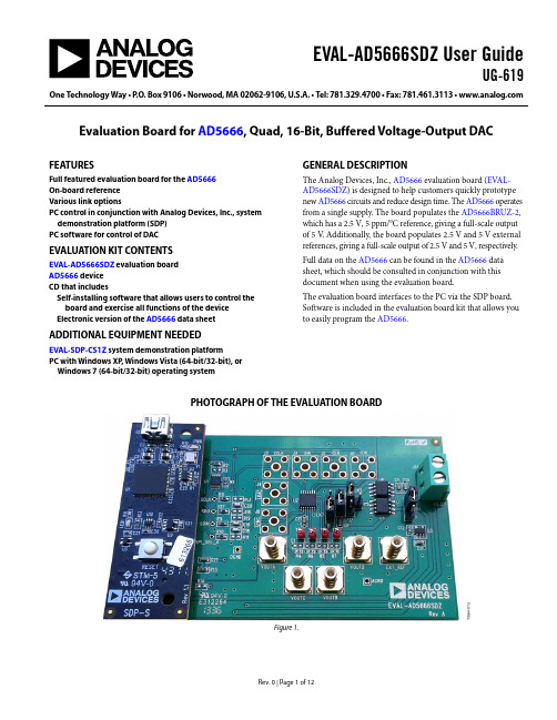
EVAL-AD5666SDZ User GuideUG-619One Technology Way • P .O. Box 9106 • Norwood, MA 02062-9106, U.S.A. • Tel: 781.329.4700 • Fax: 781.461.3113 • Evaluation Board for AD5666, Quad, 16-Bit, Buffered Voltage-Output DACFEATURESFull featured evaluation board for the AD5666 On-board reference Various link optionsPC control in conjunction with Analog Devices, Inc., system demonstration platform (SDP) PC software for control of DACEVALUATION KIT CONTENTSEVAL-AD5666SDZ evaluation board AD5666 device CD that includesSelf-installing software that allows users to control the board and exercise all functions of the device Electronic version of the AD5666 data sheetADDITIONAL EQUIPMENT NEEDEDEVAL-SDP-CS1Z system demonstration platformPC with Windows XP , Windows Vista (64-bit/32-bit), or Windows 7 (64-bit/32-bit) operating systemGENERAL DESCRIPTIONThe Analog Devices, Inc., AD5666 evaluation board (EV AL-AD5666SDZ ) is designed to help customers quickly prototype new AD5666 circuits and reduce design time. The AD5666 operates from a single supply. The board populates the AD5666BRUZ-2, which has a 2.5 V, 5 ppm/°C reference, giving a full-scale output of 5 V . Additionally, the board populates 2.5 V and 5 V external references, giving a full-scale output of 2.5 V and 5 V, respectively. Full data on the AD5666 can be found in the AD5666 data sheet, which should be consulted in conjunction with this document when using the evaluation board.The evaluation board interfaces to the PC via the SDP board. Software is included in the evaluation board kit that allows you to easily program the AD5666.PHOTOGRAPH OF THE EVALUATION BOARDFigure 1.11864-013UG-619 EVAL-AD5666SDZ User Guide TABLE OF CONTENTSFeatures (1)Evaluation Kit Contents (1)Additional Equipment Needed (1)General Description (1)Photograph of the Evaluation Board (1)Revision History (2)Evaluation Board Hardware (3)Power Supplies (3)Link Options (3)Evaluation Board Software (4)Installing the Software (4)Running the Software (4)Operating the Software (5)Evaluation Board Schematics and Artwork (7)Bill of Materials (10)REVISION HISTORY11/13—Revision 0: Initial VersionEVAL-AD5666SDZ User Guide UG-619 EVALUATION BOARD HARDWAREPOWER SUPPLIESThe AD5666 evaluation board can be powered either from the on-board regulator of 3.3 V or externally by the J14-1 and J14-2 connectors, as described in Table 1.Only an AGND connector is provided on the board. The AGND and DGND planes are connected at one point under the AD5666 device. It is recommended not to connect AGND and DGND elsewhere in the system to avoid ground loop problems. The supply is decoupled to ground with 10 µF tantalum and 0.1 µF ceramic capacitors. Table 1. Power Supply ConnectorsConnector No. Name VoltageJ14-1 +5.5V From 2.7 V to 5.5 VJ14-2 GND AGNDLINK OPTIONSBefore using the evaluation board, the link options must be set for the desired operating mode (see Table 2 for more information). By default, the evaluation board is set up to be controlled by a PC via the USB port and SDP board.Table 2. Link FunctionsLink No. Option Default Position LK1 This link selects the main board voltage source. B Position A selects the regulated voltage from the USB voltage source, 3.3 V.Position B selects the external supply voltage provided by the J14 connector.LK2 This link selects the DAC voltage reference. C Position A selects the REF195 external reference. This reference is operational only if the board is poweredexternally with a voltage higher than 5.1 V.Position B selects an off-board reference.Position C selects the REF192 external reference.LK7 This link selects the supply voltage for the AD5666. B Position A selects the source selected by LK1.Position B selects the source selected by LK2.LK8 This link adds an external capacitor on the AD5666 V REF voltage. Inserted Inserted selects the capacitor to be connected.Disconnected selects the capacitor to be disconnected.UG-619 EVAL-AD5666SDZ User Guide EVALUATION BOARD SOFTWAREINSTALLING THE SOFTWAREThe EV AL-AD5666SDZ kit includes self-installing software on a CD. The software is compatible with Windows® XP, Windows Vista (64-bit/32-bit), and Windows 7 (64-bit/32-bit).Install the software before connecting the SDP board to the USB port of the PC. This ensures that the SDP board is recognized when it is connected to the PC.1.Start the Windows operating system and insert the CD.2.The installation software should open automatically. If itdoes not, run the setup.exe file from the CD.3.After installation is completed, power up the evaluationboard as described in the Power Supplies section.4.Plug the EV AL-AD5666SDZ into the SDP board and theSDP board into the PC using the USB cable included in the evaluation board kit.5.When the software detects the evaluation board, proceedthrough any dialog boxes that appear to finalize theinstallation.RUNNING THE SOFTWARETo run the program, do the following:1.Click Start > All Programs > Analog Devices > AD5666>AD5666 Evaluation Software. (To uninstall the program, click Start > Control Panel > Add or Remove Programs > AD5666 Evaluation Software.)2.If the SDP board is not connected to the USB port whenthe software is launched, a connectivity error is displayed(see Figure 2). If a connectivity error is displayed, connect the evaluation board to the USB port of the PC and wait a few seconds, and then click Rescan and follow theinstructions.Figure 2. SDP Board to USB Port Connectivity Error Message 3.If the SDP board is not connected to the evaluation board,a message box appears as shown in Figure 3. Check theconnection between the SDP and EV AL-AD5666SDZboards and then run the program again.Figure 3. SDP Board to Evaluation Board Error Message4.When the SDP board is connected, a wait window isdisplayed briefly (see Figure 4), and then the main windowof the AD5666 evaluation software opens, as shown inFigure 5.Figure 4. System Development Platform Wait Window11864-311864-211864-4EVAL-AD5666SDZ User GuideUG-619OPERATING THE SOFTWARETo run the AD5666 GUI, click Start > All Programs > Analog Devices > AD5666 > AD5666 Evaluation Software. The AD5666 main window opens, as shown in Figure 5. The DAC Controls tab (see Figure 5) allows you to view the input register, DAC register, and output voltage (V OUT A to V OUT D). On the left side of the window, you can type ahexadecimal value into the INPUT V ALUE (Hex) box to be written to the input and/or DAC registers as follows: •Click Write to Input Register to write the value to the input register. This updates only the input register; the DAC register is not updated.• Click Update DAC Register from Input Register to update the DAC register.• Click Write to DAC Channel to simultaneously write to the input register and update the DAC register.The DAC Registers tab (see Figure 6) allows you to access theclear code register, reset register, internal reference register, LDAC register, and power-down register. Therefore, this tab allows you to change the parameters of the device and how the device performs.Hardware PinsTo set the LDAC and CLR pins to high or low, click the appropriate check box under the block diagram in the main window. This command is executed immediately.Figure 5. AD5666 Evaluation Board Main Window, DAC Controls Tab11864-006UG-619EVAL-AD5666SDZ User GuideFigure 6. AD5666 Evaluation Board Main Window, DAC Registers Tab11864-012EVAL-AD5666SDZ User Guide UG-619Figure 7. Schematic of Supply and ReferencesFigure 8. Schematic of AD5666 Evaluation CircuitryUG-619 EVAL-AD5666SDZ User GuideFigure 9. Schematic of SDP ConnectorEVAL-AD5666SDZ User Guide UG-619Figure 10. Component Placement Drawing Figure 11. Component Side PCB DrawingFigure 12. Solder Side PCB Drawing 1 1 8 6 4 -0 11 1 1 8 6 4 -0 091 1 8 6 4 -0 1 0UG-619 EVAL-AD5666SDZ User Guide BILL OF MATERIALSTable 3. EVAL-AD5666SDZ Bill of MaterialsQty Reference Designator Description Supplier/Part Number3 C18, C19, C20 Capacitor, 0603, 100 V, 100 pF Farnell 17406054 C6, C7, C9, C21 Capacitor, 0603, 25 V, 0.1 µF Farnell 18288992 C11, C12 Capacitor, 0603, 1 µF, 16 V Farnell 16588702 C9, C16 Capacitor, 0603, 10 µF, 10 V Farnell 18535384 R8, R9, R10, R17 Resistor, 0603, 33 Ω Farnell 93310501 R13 Resistor, 0603, 0 Ω Farnell 93316625 EXT_REF, VOUTA, VOUTB, VOUTC, VOUTD SMB connector Farnell 12060131 J1 120-way connector Farnell 13246601 J14 2-pin terminal block Farnell 1517892 LK1, LK2 3-pin connector Farnell 1022249 and Farnell 150411 1 LK7 3-pin connector Farnell 1022248 and Farnell 150410 1 LK8 3-pin connector Farnell 1022247 and Farnell 150411 4 TPA, TPB, TPC, TPD Test point Farnell 87311441 U1 32k I2C serial EEPROM Farnell 13313301 U2 Quad, 16-bit DAC AD5666BRUZ-21 U3 3.3 V regulator ADP121-AUJZ33R71 U4 2.5 V reference REF192GSZ1 U6 5 V reference REF195ESZ2 Screw1, Screw2 SDP screw Farnell 70705972 Nut1, Nut2 SDP nut Farnell 7061857EVAL-AD5666SDZ User Guide UG-619 NOTESRev. 0 | Page 11 of 12UG-619 EVAL-AD5666SDZ User Guide Rev. 0 | Page 12 of 12 NOTESESD CautionESD (electrostatic discharge) sensitive device . Charged devices and circuit boards can discharge without detection. Although this product features patented or proprietary protection circuitry, damage may occur on devices subjected to high energy ESD. Therefore, proper ESD precautions should be taken to avoid performance degradation or loss of functionality. Legal Terms and Conditions By using the evaluation board discussed herein (together with any tools, components documentation or support materials, the “Evaluation Board”), you are agreeing to be bound by the terms and conditions set forth below (“Agreement”) unless you have purchased the Evaluation Board, in which case the Analog Devices Standard Terms and Conditions of Sale shall govern. Do not use the Evaluation Board until you have read and agreed to the Agreement. Your use of the Evaluation Board shall signify your acceptance of the Agreement. This Agreement is made by and between you (“Customer”) and Analog Devices, Inc. (“ADI”), with its principal place of business at One Technology Way, Norwood, MA 02062, USA. Subject to the terms and conditions of the Agreement, ADI hereby grants to Customer a free, limited, personal, temporary, non-exclusive, non-sublicensable, non-transferable license to use the Evaluation Board FOR EVALUATION PURPOSES ONLY . Customer understands and agrees that the Evaluation Board is provided for the sole and exclusive purpose referenced above, and agrees not to use the Evaluation Board for any other purpose. Furthermore, the license granted is expressly made subject to the following additional limitations: Customer shall not (i) rent, lease, display, sell, transfer, assign, sublicense, or distribute the Evaluation Board; and (ii) permit any Third Party to access the Evaluation Board. As used herein, the term “Third Party” includes any entity other than ADI, Customer, their employees, affiliates and in-house consultants. The Evaluation Board is NOT sold to Customer; all rights not expressly granted herein, includingownership of the Evaluation Board, are reserved by ADI. CONFIDENTIALITY . This Agreement and the Evaluation Board shall all be considered the confidential and proprietary information of ADI. Customer may not disclose or transfer any portion of the Evaluation Board to any other party for any reason. Upon discontinuation of use of the Evaluation Board or termination of this Agreement, Customer agrees to promptly return the Evaluation Board to ADI. ADDITIONAL RESTRICTIONS. Customer may not disassemble, decompile or reverse engineer chips on the Evaluation Board. Customer shall inform ADI of any occurred damages or any modifications or alterations it makes to the Evaluation Board, including but not limited to soldering or any other activity that affects the material content of the Evaluation Board. Modifications to the Evaluation Board must comply with applicable law, including but not limited to the RoHS Directive. TERMINATION. ADI may terminate this Agreement at any time upon giving written notice to Customer. Customer agrees to return to ADI the Evaluation Board at that time. LIMITATION OF LIABILITY . THE EVALUATION BOARD PROVIDED HEREUNDER IS PROVIDED “AS IS” AND ADI MAK ES NO WARRANTIES OR REPRESENTATIONS OF ANY KIND WITH RESPECT TO IT. ADI SPECIFICALLY DISCLAIMS ANY REPRESENTATIONS, ENDORSEMENTS, GUARANTEES, OR WARRANTIES, EXPRESS OR IMPLIED, RELATED TO THE EVALUATION BOARD INCLUDING, BUT NOT LIMITED TO, THE IMPLIED WARRANTY OF MERCHANTABILITY, TITLE, FITNESS FOR A P ARTICULAR PURPOSE OR NONINFRINGEMENT OF INTELLECTUAL PROPERTY RIGHTS. IN NO EVENT WILL ADI AND ITS LICENSORS BE LIABLE FOR ANY INCIDENTAL, SPECIAL, INDIRECT, OR CONSEQUENTIAL DAMAGES RESUL TING FROM CUSTOMER’S POSSESSION OR USE OF THE EVALUATION BOARD, INCLUDING BUT NOT LIMITED TO LOST PROFITS, DELAY COSTS, LABOR COSTS OR LOSS OF GOODWILL. ADI’S TOTAL LIABILITY FROM ANY AND ALL CAUSES SHALL BE LIMITED TO THE AMOUNT OF ONE HUNDRED US DOLLARS ($100.00). EXPORT. Customer agrees that it will not directly or indirectly export the Evaluation Board to another country, and that it will comply with all applicable United States federal laws and regulations relating to exports. GOVERNING LAW. This Agreement shall be governed by and construed in accordance with the substantive laws of the Commonwealth of Massachusetts (excluding conflict of law rules). Any legal action regarding this Agreement will be heard in the state or federal courts having jurisdiction in Suffolk County, Massachusetts, and Customer hereby submits to the personal jurisdiction and venue of such courts. The United Nations Convention on Contracts for the International Sale of Goods shall not apply to this Agreement and is expressly disclaimed. ©2013 Analog Devices, Inc. All rights reserved. Trademarks andregistered trademarks are the property of their respective owners.UG11864-0-11/13(0)。
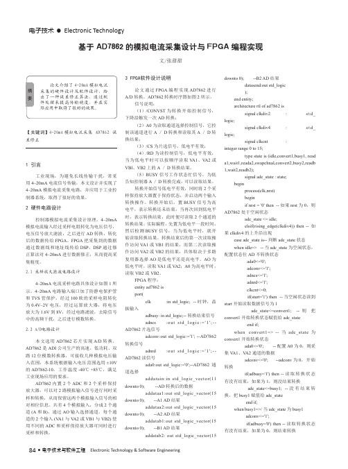
电子技术• Electronic Technology84 •电子技术与软件工程 Electronic Technology & Software Engineering【关键词】4-20mA 模拟电流采集 AD7862 误差修正1 引言工业现场,为避免长线传输干扰,常采用4~20mA 电流信号传输,本文设计并实现了4~20mA 模拟电流采集电路,并应用于工业控制器系统,取得了很好的效果。
2 硬件电路设计控制器模拟电流采集设计原理。
4~20mA 模拟电流输入经过采样电阻转化为电压信号,电压信号放大滤波,之后进行AD 转换,转化后的数据传给FPGA 。
FPGA 把采集到的数据通过数据线和地址线传给DSP ,DSP 通过修正算法对4~20mA 进行数据修正,从而提高采集精度。
2.1 采样放大滤波电路设计4~20mA 电流采样电路具体设计如图1所示。
4~20mA 电路输入端口加了防静电保护管和TVS 管保护,经过100欧的采样电阻转化为0.4V~2V 电压,经过运算放大器,将电压放大为1.6V 到8V ,经过电路滤波,去除信号中的高频干扰,之后进行模数转换。
2.2 A/D电路设计本文选用AD7862芯片实现A/D 转换。
AD7862是ADI 公司生产的高速、低功耗、双路12位模数转换器,可接收几种模拟电压输入范围,本系统根据输入电压范围选用±10V 的AD7862-10。
工作温度-40℃+85℃,满足工业现场应用的要求。
AD7862内置2个ADC 和2个采样保持放大器,可以对2路模拟输入信号进行同时采样和转换,从而保留这两个模拟输入信号的相对相位信息。
共有4个模拟输入,分成2个通道(A 和B),通过AO 输入选择通道。
每个通道的2个输入(V A1与V A2或VB1与VB2)使用不同的ADC 和采样保持放大器可同时进行采样和转换。
基于AD7862的模拟电流采集设计与FPGA 编程实现文/张甜甜3 FPGA软件设计说明论文通过FPGA 编程实现AD7862进行A/D 转换。
4-20毫安信号转为热电偶信号模块在工业自动化、过程控制等领域,信号传输与转换起着关键作用。
其中,4-20毫安(MA)信号和热电偶信号是常见的两种信号类型。
为了实现多种信号之间的互通,了解如何将4-20毫安信号转换为热电偶信号显得尤为重要。
4-20毫安信号是一种线性模拟信号,通常用于传感器输出,它能直观地反映被测量的物理量大小。
而热电偶信号是一种温度传感器输出信号,它能直接测量物体的温度。
在很多实际应用场景中,需要将4-20毫安信号转换为热电偶信号,以便更好地满足温度控制需求。
转换原理及方法:4-20毫安信号转换为热电偶信号的关键是将电流信号转化为温度信号。
具体转换方法如下:1.首先,对4-20毫安信号进行放大处理,使其满足热电偶传感器的要求。
通常,需要将电流信号放大到几十至几百毫安范围内。
2.接着,将放大后的电流信号输入到热电偶传感器中,传感器会将电流信号转换为相应的温度值。
3.最后,对热电偶传感器输出的温度信号进行处理,将其转换为所需的格式,如数字信号或PID控制信号。
在转换过程中,需要注意以下几点:1.确保4-20毫安信号的准确性,避免信号干扰和衰减。
2.选择合适的热电偶类型和连接方式,以保证温度测量的准确性。
3.对热电偶传感器进行校准,以消除系统误差。
4.考虑信号转换装置的稳定性和可靠性,确保长期稳定运行。
应用场景及优势:4-20毫安信号转换为热电偶信号在工业自动化、科研、环境保护等领域具有广泛的应用。
通过转换,可以实现对温度的精确控制,提高生产效率,降低能耗。
同时,热电偶信号具有较高的抗干扰能力和稳定性,有助于提高整个系统的可靠性。
结论:4-20毫安信号转为热电偶信号在实际应用中具有重要意义。
掌握转换原理和方法,注意过程中的关键环节,有助于实现高效、精确的温度控制。

Rev. EDocument FeedbackInformation furnished by Analog Devices is believed to be accurate and reliable. However, no responsibility is assumed by Analog Devices for its use, nor for any infringements of patents or other rights of third parties that may result from its use. Specifications subject to change without notice. No license is granted by implication or otherwise under any patent or patent rights of Analog Devices. Trademarks andregistered trademarks are the property of their respective owners.One Technology Way, P .O. Box 9106, Norwood, MA 02062-9106, U.S.A.Tel: 781.329.4700 ©2008-2016 Analog Devices, Inc. All rights reserved. Technical Support /cnADI 中文版数据手册是英文版数据手册的译文,敬请谅解翻译中可能存在的语言组织或翻译错误,ADI 不对翻译中存在的差异或由此产生的错误负责。
如需确认任何词语的准确性,请参考ADI 提供的最1.2 A 可编程器件电源, 集成16位电平设置DAC数据手册AD5560特性可编程器件电源(DPS) FV 、MI 、MV 、FNMV 功能 5种内部电流范围(片内R SENSE )±5 µA 、±25 µA 、±250 µA 、±2.5 mA 、±25 mA 2种外部高电流范围(外部R SENSE ) EXTFORCE1:±1.2 A (最大值) EXTFORCE2:±500 mA (最大值) 集成可编程电平全部为16位DAC :驱动DAC 、比较器DAC 、箝位DAC 、偏置DAC 、OSD DAC 、DGS DAC 可编程开尔文箝位和报警 片内集成偏置和增益校正寄存器 驱动DAC 提供电源斜坡摆率可调 可编程压摆率特性:1 V/μs 至0.3 V/μs DUTGND 开尔文检测和报警25 V FV 跨度,可在−22 V 至+25 V 范围内非对称工作片内集成比较器GANG 模式:可联合多个器件以提供更高的电流 带有Guard 驱动放大器 支持系统PMU 连接 电流箝位带芯片温度传感器和关断特性 片内集成二极管测温阵列 可通过诊断寄存器访问内部节点开漏报警标志(温度、电流箝位、开尔文报警) SPI/MICROWIRE/DSP 兼容型接口64引脚(10 mm × 10 mm)TQFP 封装,带裸露焊盘(顶部) 72引脚(8 mm × 8 mm)倒装芯片BGA 封装应用自动测试设备(ATE) 器件电源概述AD5560是一款高性能、高集成度器件电源,提供可编程的驱动电压和测量范围。
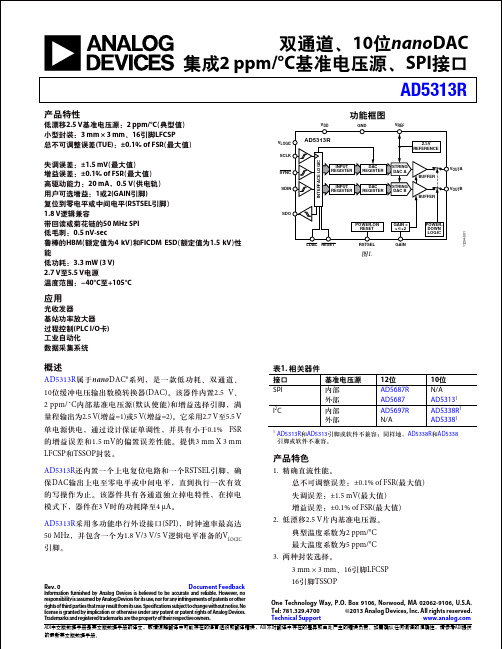
Rev. 0Document Feedback Information furnished by Analog Devices is believed to be accurate and reliable. However, noresponsibility is assumed by Analog Devices for its use, nor for any infringements of patents or other rights of third parties that may result from its use. Speci cations subject to change without notice. No license is granted by implication or otherwise under any patent or patent rights of Analog Devices. T rademarks and registered trademarks are the property of their respective owners. One Technology Way, P.O. Box 9106, Norwood, MA 02062-9106, U.S.A. Tel: 781.329.4700 ©2013 Analog Devices, Inc. All rights reserved. Technical Support 功能框图图1.表1. 相关器件接口基准电压源12位10位SPI 内部AD5687R N/A外部AD5687 AD53131I2C 内部AD5697R AD5338R1外部N/A AD533811AD5313R和AD5313引脚或软件不兼容;同样地,AD5338R和AD5338引脚或软件不兼容。
SCLKV LOGICSYNCSDINSDOINPUTREGISTERDACREGISTERSTRINGDAC ABUFFERV OUT AINPUTREGISTERDACREGISTERSTRINGDAC BBUFFERV OUT BV REFGNDV DDPOWER-DOWNLOGICPOWER-ONRESETGAIN =×1/×2INTERFACELOGICRSTSEL GAINLDAC RESETAD5313R2.5VREFERENCE11254-1双通道、10位nano DAC集成2 ppm/°C基准电压源、SPI接口AD5313R 产品特性低漂移2.5 V基准电压源:2 ppm/°C(典型值)小型封装:3 mm × 3 mm、16引脚LFCSP总不可调整误差(TUE):±0.1% of FSR(最大值)失调误差:±1.5 mV(最大值)增益误差:±0.1% of FSR(最大值)高驱动能力:20 mA,0.5 V(供电轨)用户可选增益:1或2(GAIN引脚)复位到零电平或中间电平(RSTSEL引脚)1.8 V逻辑兼容带回读或菊花链的50 MHz SPI低毛刺:0.5 nV-sec鲁棒的HBM(额定值为4 kV)和FICDM ESD(额定值为1.5 kV)性能低功耗:3.3 mW (3 V)2.7 V至5.5 V电源温度范围:−40°C至+105°C应用光收发器基站功率放大器过程控制(PLC I/O卡)工业自动化数据采集系统概述AD5313R属于nano DAC®系列,是一款低功耗、双通道、10位缓冲电压输出数模转换器(DAC)。
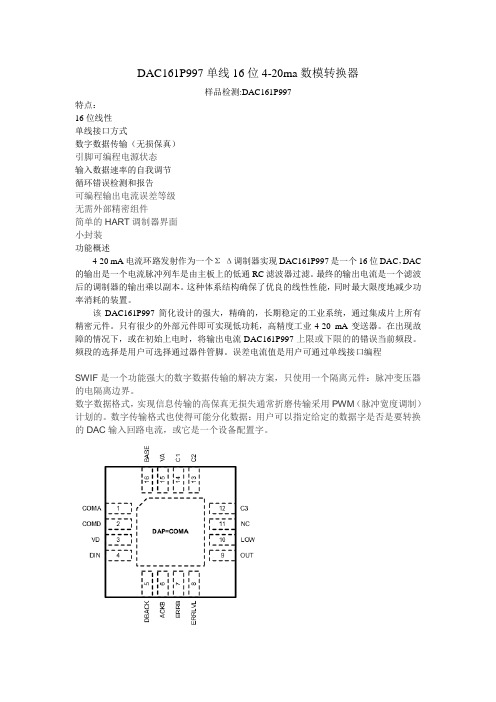
DAC161P997单线16位4-20ma数模转换器
样品检测:DAC161P997
特点:
16位线性
单线接口方式
数字数据传输(无损保真)
引脚可编程电源状态
输入数据速率的自我调节
循环错误检测和报告
可编程输出电流误差等级
无需外部精密组件
简单的HART调制器界面
小封装
功能概述
4-20 mA电流环路发射作为一个Σ-Δ调制器实现DAC161P997是一个16位DAC,DAC 的输出是一个电流脉冲列车是由主板上的低通RC滤波器过滤。
最终的输出电流是一个滤波后的调制器的输出乘以副本。
这种体系结构确保了优良的线性性能,同时最大限度地减少功率消耗的装置。
该DAC161P997简化设计的强大,精确的,长期稳定的工业系统,通过集成片上所有精密元件。
只有很少的外部元件即可实现低功耗,高精度工业4-20 mA变送器。
在出现故障的情况下,或在初始上电时,将输出电流DAC161P997上限或下限的的错误当前频段。
频段的选择是用户可选择通过器件管脚。
误差电流值是用户可通过单线接口编程
SWIF是一个功能强大的数字数据传输的解决方案,只使用一个隔离元件:脉冲变压器的电隔离边界。
数字数据格式,实现信息传输的高保真无损失通常折磨传输采用PWM(脉冲宽度调制)计划的。
数字传输格式也使得可能分化数据:用户可以指定给定的数据字是否是要转换的DAC输入回路电流,或它是一个设备配置字。
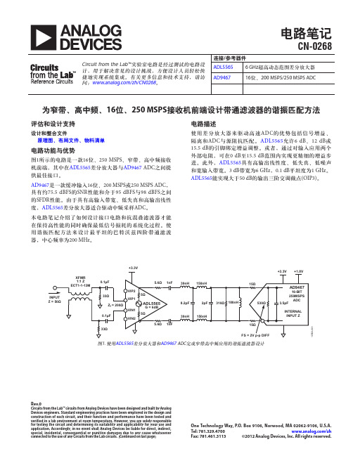
为窄带、高中频、16位、250 MSPS 接收机前端设计带通滤波器的谐振匹配方法评估和设计支持设计和整合文件原理图、布局文件、物料清单电路功能与优势图1所示的电路是一款16位、250 MSPS 、窄带、高中频接收机前端,其中在ADL5565差分放大器与AD9467 ADC 之间提供最佳接口。
AD9467是一款缓冲输入16位、200 MSPS 或250 MSPS ADC ,具有约75.5 dBFS 的SNR 性能和介于95 dBFS 与98 dBFS 之间的SFDR 性能。
由于具有高输入带宽、低失真和高输出线性度,ADL5565差分放大器适合驱动中频采样ADC 。
本电路笔记介绍了如何设计接口电路和抗混叠滤波器才能在保持高性能的同时确保最低信号损耗的系统化过程。
使用谐振匹配方法来设计最平坦的巴特沃兹四阶带通滤波器,中心频率为200 MHz 。
电路描述使用差分放大器来驱动高速ADC 的优势包括信号增益、隔离和ADC 与源阻抗匹配。
ADL5565允许6 dB 、12 dB 或 15.5 dB 的引脚绑定增益调整。
或者,通过对输入应用两个外部电阻,可在0 dB 至15.5 dB 范围内实现更精细的增益步进。
此外,ADL5565具有高输出线性度、低失真、低噪声和宽输入带宽。
3 dB 带宽为6 GHz ,0.1 dB 平坦度为1 GHz 。
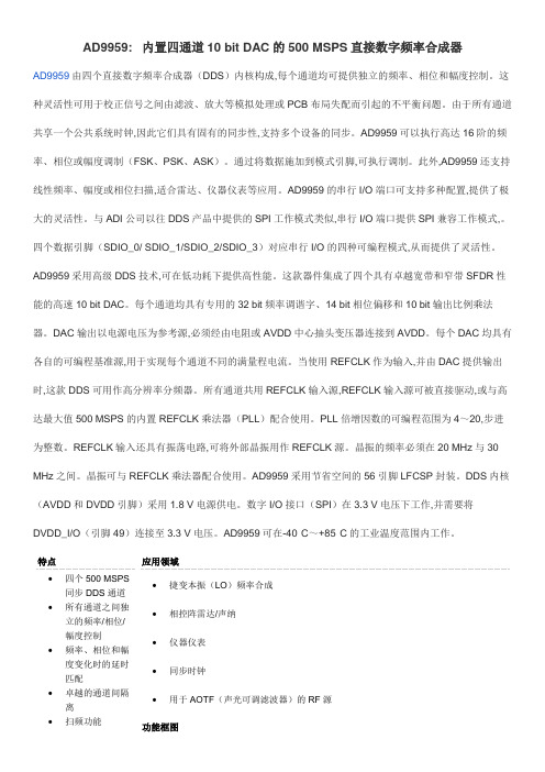
ADL5565能实现大于50 dB 的输出三阶交调截点(OIP3)。
10560-001图1. 使用ADL5565差分放大器和AD9467 ADC 完成窄带高中频应用的谐振滤波器设计电路笔记Rev.0Circuits from the Lab™ circuits from Analog Devices have been designed and built by Analog Devices engineers. Standard engineering practices have been employed in the design and construction of each circuit, and their function and performance have been tested and verified in a lab environment at room temperature. However, you are solely responsible for testing the circuit and determining its suitability and applicability for your use and application. Accordingly, in no event shall Analog Devices be liable for direct, indirect, special, incidental, consequential or punitive damages due to any cause whatsoever connected to the use of any Circuits from the Lab circuits. (Continued on last page)One Technology Way, P .O. Box 9106, Norwood, MA 02062-9106, U.S.A. Tel: 781.329.4700 /zh Fax: 781.461.3113 ©2012 Analog Devices, Inc. All rights reserved.为实现ADL5565和AD9467必须提供的最佳性能水平,必须严格遵循各数据手册中指定的设计原则。
AD9959: 内置四通道10 bit DAC的500 MSPS直接数字频率合成器AD9959由四个直接数字频率合成器(DDS)内核构成,每个通道均可提供独立的频率、相位和幅度控制。
这种灵活性可用于校正信号之间由滤波、放大等模拟处理或PCB布局失配而引起的不平衡问题。
由于所有通道共享一个公共系统时钟,因此它们具有固有的同步性,支持多个设备的同步。
AD9959可以执行高达16阶的频率、相位或幅度调制(FSK、PSK、ASK)。
通过将数据施加到模式引脚,可执行调制。
此外,AD9959还支持线性频率、幅度或相位扫描,适合雷达、仪器仪表等应用。
AD9959的串行I/O端口可支持多种配置,提供了极大的灵活性。
与ADI公司以往DDS产品中提供的SPI工作模式类似,串行I/O端口提供SPI兼容工作模式,。
四个数据引脚(SDIO_0/ SDIO_1/SDIO_2/SDIO_3)对应串行I/O的四种可编程模式,从而提供了灵活性。
AD9959采用高级DDS技术,可在低功耗下提供高性能。
这款器件集成了四个具有卓越宽带和窄带SFDR性能的高速10 bit DAC。
每个通道均具有专用的32 bit频率调谐字、14 bit相位偏移和10 bit输出比例乘法器。
DAC 输出以电源电压为参考源,必须经由电阻或AVDD中心抽头变压器连接到AVDD。
每个DAC均具有各自的可编程基准源,用于实现每个通道不同的满量程电流。
当使用REFCLK作为输入,并由DAC提供输出时,这款DDS 可用作高分辨率分频器。
所有通道共用REFCLK输入源,REFCLK输入源可被直接驱动,或与高达最大值500 MSPS的内置REFCLK乘法器(PLL)配合使用。
PLL倍增因数的可编程范围为4~20,步进为整数。
REFCLK 输入还具有振荡电路,可将外部晶振用作REFCLK源。
晶振的频率必须在20 MHz与30 MHz之间。
晶振可与REFCLK乘法器配合使用。
ADI 16bit DAC的速率倍增到每秒10亿次采样
佚名
【期刊名称】《电子产品世界》
【年(卷),期】2005(000)03A
【摘要】ADI发布业界首款采样速率达到1GSPS的16bit数模转换器(DAC),这一速率是同类产品的两倍。
作为双通道DAC,AD9779能够保证增益和失调的匹配,从而使其适用于采用一个模拟正交调制器的直接转换或镜像抑制体系结构。
AD9779适合于用作诸如W—CDMA,CDMA2000,
【总页数】1页(P134)
【正文语种】中文
【中图分类】TN792
【相关文献】
1.ADI推出业界最小封装16bit四DAC AD5664R [J],
2.ADI推出业界最小封装16bit四DAC AD5664R [J], 章从福;
3.ADI公司16 bit DAC的速率倍增到每秒10亿次采样 [J],
4.ADI公司16bit DAC的速率倍增到10亿次/s采样 [J],
5.16bit,10MS/sSAR模数转换器具有15bit有效位数(ENOB)及2.5倍的采样速率[J],
因版权原因,仅展示原文概要,查看原文内容请购买。
CN0009 利用ADI AD5662 DAC 实现4 mA 至20 mA
过程控制环路
电路功能与优势
在许多过程控制应用中,经常使用两线式电流发射器在高噪声环境中传输
模拟信号。
这些电流发射器的零电平信号电流为 4 mA,满量程信号电流为20 mA,因此得名“4 mA 至20 mA 转换器”。
本文所述电路提供一种具有16 位分辨率和单调性的低功耗电流发射器,它直接采用 4 mA 至20 mA 控制环路电源供电,功耗低于 4 mA。
功耗高于 4 mA 的发射器无法直接采用环路电源供电,因而需要一个附加电源。
电路描述
AD5662 本电路将nanoDAC 转换器用作控制器,提供 4 mA 至20 mA 可编程输出电流。
环路电流通过测量RS 上的压降VOUT 进行检测。
如果DAC 输
出为0 V,则电流
其中0 ≤D ≤65,535。
当AD5662 的数字码等于0xFFFF 时,本电路提供20.9 mA 满量程输出电流。
同样,当AD5662 的数字码等于0x0000 时,输出电流将为3.49 mA。
扩展电流范围(3.49 mA 至20.9 mA)允许用户利用软件和AD5662 的16 位分辨率校准 4 mA 至20 mA 范围。
本电路需要使用肖特基二极管,以防止环路电源上电瞬态将AD8627 的同相输入端拉至反相输入端300 mV 以下。
该肖特基二极管必须能够处理至少20 mA 的全环路负载。