3rd Reid ch14
- 格式:ppt
- 大小:1.88 MB
- 文档页数:39
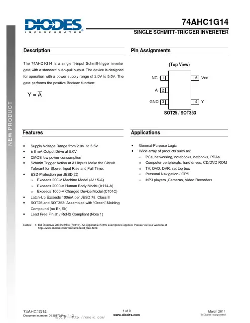
DescriptionThe 74AHC1G14 is a single 1-input Schmitt-trigger inverter gate with a standard push-pull output. The device is designed for operation with a power supply range of 2.0V to 5.5V. The gate performs the positive Boolean function:AY =Pin AssignmentsSOT25 / SOT353NCGND YVcc(Top View)AFeatures• Supply Voltage Range from 2.0V to 5.5V • ± 8 mA Output Drive at 5.0V • CMOS low power consumption• Schmitt Trigger Action at All Inputs Make the Circuit Tolerant for Slower Input Rise and Fall Time. •ESD Protection per JESD 22o Exceeds 200-V Machine Model (A115-A) o Exceeds 2000-V Human Body Model (A114-A) o Exceeds 1000-V Charged Device Model (C101C) • Latch-Up Exceeds 100mA per JESD 78, Class II • SOT25 and SOT353: Assembled with “Green” Molding Compound (no Br, Sb)• Lead Free Finish / RoHS Compliant (Note 1)Applications• General Purpose Logic •Wide array of products such as:o PCs, networking, notebooks, netbooks, PDAs o Computer peripherals, hard drives, CD/DVD ROM o TV, DVD, DVR, set top box o Personal Navigation / GPSo MP3 players ,Cameras, Video RecordersNotes: 1. EU Directive 2002/95/EC (RoHS). All applicable RoHS exemptions applied. Please visit our website at/products/lead_free.html .Pin DescriptionsPin NamePin NO.DescriptionNC 1 NoConnection A 2 Data Input GND 3 Ground Y 4 Data OutputV CC 5 Supply VoltageLogic DiagramFunction TableInputs Output AYH L L HAbsolute Maximum Ratings (Note 2)Symbol Description Rating UnitESD HBM Human Body Model ESD Protection 2 KVESD CDM Charged Device Model ESD Protection 1 KVESD MM Machine Model ESD Protection 200 V V CC Supply Voltage Range -0.5 to 6.5 VV I Input Voltage Range -0.5 to 6.5 VV O Voltage applied to output in high or low state -0.5 to V CC +0.5 VI IK Input Clamp Current V I<0 -20 mAI OK Output Clamp Current (V O < 0 or V O > V CC) ±20 mAI O Continuous output current (V O = 0 to V CC) ±25 mAI CC Continuous current through V CC 50 mAI GND Continuous current through GND -50 mAT J Operating Junction Temperature -40 to 150 °CT STG Storage Temperature -65 to 150 °CNotes: 2. Stresses beyond the absolute maximum may result in immediate failure or reduced reliability. These are stress values and device operation should bewithinrecommendvalues.Recommended Operating Conditions (Note 3)Symbol Parameter Min Max UnitV CC Operating Voltage 2 5.5 V V I Input Voltage 0 5.5 VV O Output Voltage 0 V CC VI OH High-level output current V CC = 2V -50 uA V CC = 3.3V ± 0.3V -4mAV CC = 5V ± 0.5V -8I OL Low-level output current V CC = 2V 50 uA V CC = 5V ± 0.5V 4mAV CC = 3V 8T A Operating free-airtemperature-40 125 ºCNotes: 3. Unused inputs should be held at V CC or Ground.Electrical CharacteristicsSymbol Parameter Test Conditions V CC25ºC -40ºC to 85ºC -40ºC to 125ºCUnit Min Typ. Max Min Max Min MaxV T+Positive-goinginputthresholdvoltage3V 2.2 2.2 2.2 V4.5V 3.15 3.15 3.15 V5.5V 3.85 3.85 3.85 VV T-Negative-goinginputthresholdvoltage3 V 0.9 0.9 0.9 V4.5V 1.35 1.35 1.35 V5.5V 1.65 1.65 1.65 VΔV T Hysteresis(V T+ - V T-)3V 0.3 1.2 0.3 1.2 0.25 1.2 V4.5V 0.4 1.4 0.4 1.4 0.35 1.4 V5.5V 0.5 1.6 0.5 1.6 0.45 1.6V OH High LevelOutput VoltageI OH = -50μA2V 1.9 2 1.9 1.9V3V 2.9 3 2.9 2.94.5V 4.4 4.5 4.4 4.4I OH = -4mA 3V 2.58 2.48 2.40I OH = -8mA 4.5V 3.94 3.8 3.70V OL Low LevelOutput VoltageI OL = 50μA2V 0.1 0.1 0.1V3V 0.1 0.1 0.14.5V 0.1 0.1 0.1I OL = 4mA 3V 0.36 0.44 0.55I OL = 8mA 4.5V 0.36 0.44 0.55I I Input Current V I = 5.5 V or GND 0 to 5.5V± 0.1 ± 1 ± 2 μAI CC Supply Current V I = 5.5V or GNDI O=05.5V 1 10 40 μAC I InputCapacitanceV I = V CC – orGND5.5V 2.0 10 10 10 pFθJA ThermalResistanceJunction-to-AmbientSOT25(Note 4)195o C/W SOT353 430θJC ThermalResistanceJunction-to-CaseSOT25(Note 4)58o C/W SOT353 155Note: 4. Test conditions for SOT25, and SOT353: Device mounted on FR-4 substrate PC board, 2oz copper, with minimum recommended pad layoutSwitching CharacteristicsV CC = 3.3V ± 0.3 (see Figure 1)ParameterFrom (Input) TO (OUTPUT)25ºC -40ºC to 85ºC -40ºC to 125ºCUnitMinTyp.MaxMin Max Min Maxt pdA YC L =15pF0.6 4.2 12.8 0.6 15.0 0.6 16.5 ns C L =50pF0.6 6.0 16.3 0.6 18.5 0.6 20.5 nsV CC = 5V ± 0.5V (see Figure 1)ParameterFrom (Input) TO (OUTPUT)25ºC -40ºC to 85ºC -40ºC to 125ºCUnitMinTyp.MaxMin MaxMin Maxt pdA YC L =15pF0.6 3.2 8.6 0.6 10.0 0.6 11.0 ns C L =50pF0.6 4.6 10.6 0.6 12.0 0.6 13.5 nsOperating CharacteristicsT A = 25 ºCParameterTest Conditions V CC = 5 V Unit Typ. C pdPower dissipation capacitancef = 1 MHz No Load10pFParameter Measurement InformationV CCInputsV M C LVIt r /tf3.3V±0.3VV CC ≤3ns V CC /2 15pF 5V±0.5V V CC ≤3ns V CC /2 15pF 3.3V±0.3V V CC ≤3ns V CC /2 50pF 5V±0.5VV CC≤3nsV CC /250pFVoltage Waveform Pulse DurationVoltage Waveform Propagation Delay TimesInverting and Non Inverting OutputsFigure 1. Load Circuit and Voltage WaveformsNotes: A. Includes test lead and test apparatus capacitance.B. All pulses are supplied at pulse repetition rate ≤ 1 MHz.C. Inputs are measured separately one transition per measurement.D. t PLH and t PHL are the same as t PD .Ordering Information74AHC1G 14XX -7W5:SOT25FunctionPackage7:Tape &ReelPacking 14:1-InputSchmitt-Trigger InverterSE :SOT353Logic Device 74:Logic Prefix AHC :2to Family 1G :One gate5.5VDevice Package Code Packaging (Note 5) 7” Tape and ReelQuantityPart Number Suffix74AHC1G14W5-7 W5 SOT25 3000/Tape & Reel -7 74AHC1G14SE-7SESOT3533000/Tape & Reel-7Notes: 5. Pad layout as shown on Diodes Inc. suggested pad layout document AP02001, which can be found on our website at/datasheets/ap02001.pdf.Marking InformationXX : Identification codeW : Week : A~Z : 1~26 week;X : A~Z : Internal code(Top View)Y : Year 0~9a~z : 27~52 week; z represents 52 and 53 weekPart NumberPackageIdentification Code74AHC1G14W5 SOT25 YV 74AHC1G14SE SOT353YVPackage Outline Dimensions (All Dimensions in mm) (1) Package Type: SOT25(2) Package Type: SOT353SOT25Dim Min Max TypA0.350.500.38B 1.50 1.70 1.60C 2.70 3.00 2.80D ⎯ ⎯ 0.95H 2.90 3.10 3.00J0.0130.100.05K 1.00 1.30 1.10L0.350.550.40M0.100.200.15N0.700.800.75α 0° 8° ⎯All Dimensions in mmSOT353Dim Min MaxA0.10 0.30B 1.15 1.35C 2.00 2.20D0.65 TypF0.40 0.45H 1.80 2.20J0 0.10K0.90 1.00L0.25 0.40M0.10 0.22α 0° 8°All Dimensions in mm。

1. SIMRAD_logo_2015_CMYK.eps2. SIMRAD_logo_2015_RGB.png3. SIMRAD_logo_2015_PMS1797.eps4. SIMRAD_logo_2015_mono-black.eps5. SIMRAD_logo_2015_mono-white.eps6. SIMRAD_logo_2015-keyline_CMYK.eps7. SIMRAD_logo_2015-keyline_PMS1797.png8. SIMRAD_logo_2015-keyline_RGB.eps9. SIMRAD_logo_2015-GWC-grey_CMYK.eps 10. SIMRAD_logo_2015-GWC-grey_RGB.png11. SIMRAD_logo_2015-GWC-grey_PMS.e12. SIMRAD_logo_2015-GWC-White_CMYK.eps 13. SIMRAD_logo_2015-GWC-White_RGB.png 14. SIMRAD_logo_2015-GWC-White_PMS15. SIMRAD_logo_2015-GWC-keylinewhite_CMYK.eps 16. SIMRAD_logo_2015-GWC-keylinewhite_RGB.png 17. SIMRAD_logo_2015-GWC-keylinewhit PMS.eps18. SIMRAD_tab-logo_2015-GWC-grey_CMYK.eps 19. SIMRAD_tab-logo_2015-GWC-grey_PMS.png 20. SIMRAD_tab-logo_2015-GWC-grey_PM eps21. SIMRAD_tab-logo_2015-GWC-white_CMYK.22. SIMRAD_tab-logo_2015-GWC-white_PMS.23. SIMRAD_tab-logo_2015-GWC-white_PThe Simrad E5024 ECDIS system is an IMO type-approved navigation system, designed for use aboard SOLAS vessels including large passenger ships, tankers, and cargo ships subject to the ECDIS Carriage Mandate. Ideal for vessels required to retrofit ECDIS to meet amended SOLAS requirements, themodular E5024 ECDIS system offers simple installation in either single-station or dual-station(PLECDIS) configurations.Main Features•24-inch, Full-HD 16:9 widescreen for large, clear charts• Wireless trackball controller with on-screenkeyboard• Rapid access to critical features with quick access tiles• Simplified route planning with drag-and-drop manipulation of waypoints•Radar, AIS & ARPA overlay (Simrad Argus Radar compatible)• Designed for NAVTOR ENCs including UKHO (for AVCS), Primar, IC-ENC, and NOAA• Third-party chart support with S-57 and S-63 import • Choose between S-52 and INT1 chart presentation •Supports AIO (Admiralty Information Overlay)• Simple dual-station PLECDIS option Simrad Performance Module Support with Optional Second StationThe E5024 ECDIS system includes support for an optional secondary display station, delivering complete control of Ethernet-connected Simrad performance modules including radar, conventional echosounders, ForwardScan™ sonar, and StructureScan Imaging™, in addition to third-party accessories such as FLIR cameras, CCTV, engine sensors, and other digital instrumentation.Any 16-, 19-, or 24-inch Simrad marine monitor may be used for this second station, which offers completely independent operation from the E5024 system’s type-approved ECDIS functionality.Simrad E5024 ECDIS SystemWheelmark ApprovedTechnical specifications overleaf./commercialTechnical SpecificationsSingle Processor - 1 ScreenSingle Processor - 2 Screensuu 1 x Type Approved ECDIS+uu 1 x Radar or1 x Echosounder or 1 x InstrumentsRadarOrOrECDIS E5024Touchscreen orOP40 ControllerEchosounderInstrumentsECDIS E5000 System with independent 2ndOutput for Multidisplay FunctionECDIS E50241234Simrad® logo: 201Please ensure that anincludes a registeredIn addition, the first and any prominent us。

派克汉尼汾公司版权所有未经许可不能摘录,翻印。
保留修改权利2021年6月警告销售条件本样本中产品和/或系统或相关产品出现故障,选型不当或使用不当,均可能导致人身伤亡和财产损失。
本文档以及由派克·汉尼汾公司及其子公司和授权经销商提供的其他资料,为具有技术知识的用户提供进一步研究所需的产品和/或系统选项。
重要的是,用户必须对您的应用进行全面的分析,并对当前产品样本中与产品或系统相关的资料进行评估。
由于工作条件以及产品或系统的多样性,用户必须自行分析和测试,并独自承担一切后果,包括:产品和系统的最终选型以及确保满足应用的所有性能、安全和警告等方面的要求。
派克·汉尼汾及其子公司可能会随时对本样本中的产品,包括但不限于:产品的特性、产品的规格、产品的结构、产品的有效性以及产品的价格作出变更而不另行通知.本样本中的所有产品均由派克·汉尼汾公司及其子公司和援权经销商销售。
与派克签订的任何销售合同均按照派克标准条件和销售条件中规定的条款执行(提供复印件备索)。
本公司的密封件,只能在本公司的文件资料述及的应用参数范围与接触介质、压力、温度和存放时间相一致的情况下才能使用。
在规定的应用参数范围外使用以及错误选用不同的材料都可能导致密封件寿命的缩短以及设备的损坏,甚至更严重的后果(如生命安全,环境污染等)。
样本中所列出的工作压力、温度范围、运动速度是极限值,它们之间相互关联、相互影响;在极端的工况下,建议不要同时把各个参数都同时用到极限值。
对于特殊的要求(压力、温度、速度、介质等),请联系派克汉尼汾公司以咨询合适的密封结构、材料、配置、安装建议等。
由于诸多工作参数会影响到流体传动系统及密封元件,这些设备的制造商必须在实际工作条件下测试、验证并批准密封系统的功能与可靠性。
此外,对于不断出现的新的介质(液压油、润滑脂、清洗剂等),用户特别注意它们与目前所用的密封件弹性体材料的兼容性。
我们建议用户在大批量应用之前,在厂内或现场先做密封材料的兼容性能测试,作为密封产品与系统供应商,我们建议用户遵循我们的这些建议。
1. General description74HC1G14 and 74HCT1G14 are high-speed Si-gate CMOS devices. They provide aninverting buffer function with Schmitt trigger action. These devices are capable oftransforming slowly changing input signals into sharply defined, jitter-free output signals.The HC device has CMOS input switching levels and supply voltage range 2 V to 6 V.The HCT device has TTL input switching levels and supply voltage range 4.5 V to 5.5 V.The standard output currents are half of those of the 74HC14 and 74HCT14.2. Features and benefits⏹Symmetrical output impedance ⏹High noise immunity ⏹Low power dissipation⏹Balanced propagation delays⏹SOT353-1 and SOT753 package options ⏹Specified from -40 ︒C to +125 ︒C3. Applications⏹Wave and pulse shapers ⏹Astable multivibrators ⏹Monostable multivibrators4. Ordering information74HC1G14; 74HCT1G14Inverting Schmitt triggerRev. 6 — 27 December 2012Product data sheetTable 1.Ordering informationType numberPackageTemperature rangeName DescriptionVersion 74HC1G14GW -40 ︒C to +125 ︒CTSSOP5plastic thin shrink small outline package;5leads; body width 1.25mmSOT353-174HCT1G14GW 74HC1G14GV -40 ︒C to +125 ︒CSC-74Aplastic surface-mounted package; 5 leadsSOT75374HCT1G14GV5. MarkingTable 2.Marking codesType number Marking code[1]74HC1G14GW HF74HCT1G14GW TF74HC1G14GV H1474HCT1G14GV T14[1]The pin 1 indicator is located on the lower left corner of the device, below the marking code.6. Functional diagram7. Pinning information7.1Pinning7.2Pin descriptionTable 3.Pin descriptionSymbol Pin Descriptionn.c.1not connectedA2data inputGND3ground (0 V)Y4data outputV CC5supply voltage8. Functional descriptionTable 4.Function tableH = HIGH voltage level; L = LOW voltage levelInput OutputA YL HH L9. Limiting valuesTable 5.Limiting valuesIn accordance with the Absolute Maximum Rating System (IEC 60134). Voltages are referenced to GND (ground = 0 V). [1] Symbol Parameter Conditions Min Max UnitV CC supply voltage-0.5+7.0VI IK input clamping current V I <-0.5V or V I>V CC+ 0.5V-±20mAI OK output clamping current V O<-0.5V or V O>V CC+ 0.5V-±20mAI O output current-0.5 V < V O<V CC+0.5V-±12.5mAI CC supply current-25mAI GND ground current-25-mAT stg storage temperature-65+150︒CP tot total power dissipation T amb = -40︒C to+125 ︒C[2]-200mW[1]The input and output voltage ratings may be exceeded if the input and output current ratings are observed.[2]Above 55︒C, the value of P tot derates linearly with 2.5mW/K.10. Recommended operating conditionsTable 6.Recommended operating conditionsVoltages are referenced to GND (ground = 0 V).Symbol Parameter Conditions74HC1G1474HCT1G14UnitMin Typ Max Min Typ MaxV CC supply voltage 2.0 5.0 6.0 4.5 5.0 5.5VV I input voltage0-V CC0-V CC VV O output voltage0-V CC0-V CC VT amb ambient temperature-40+25+125-40+25+125︒C11. Static characteristicsTable 7.Static characteristicsVoltages are referenced to GND (ground = 0 V). All typical values are measured at T amb=25︒C.Symbol Parameter Conditions-40︒C to+85 ︒C-40︒C to+125 ︒C UnitMin Typ Max Min MaxFor type 74HC1G14V OH HIGH-level outputvoltage V I= V T+ or V T-I O= -20μA; V CC=2.0V 1.9 2.0- 1.9-V I O= -20μA; V CC=4.5V 4.4 4.5- 4.4-V I O= -20μA; V CC=6.0V 5.9 6.0- 5.9-V I O= -2.0mA; V CC=4.5V 4.13 4.32- 3.7-V I O= -2.6mA; V CC=6.0V 5.63 5.81- 5.2-VV OL LOW-level outputvoltage V I= V T+ or V T-I O= 20μA; V CC=2.0V-00.1-0.1V I O= 20μA; V CC=4.5V-00.1-0.1V I O= 20μA; V CC=6.0V-00.1-0.1V I O= 2.0mA; V CC=4.5V-0.150.33-0.4V I O= 2.6mA; V CC=6.0V-0.160.33-0.4VI I input leakage current V I=V CC or GND; V CC=6.0V-- 1.0- 1.0μA I CC supply current V I=V CC or GND; I O=0A;V CC=6.0V--10-20μA C I input capacitance- 1.5---pFV T+positive-goingthreshold voltage see Figure7 and Figure8V CC=2.0 V0.7 1.09 1.50.7 1.5V V CC=4.5 V 1.7 2.36 3.15 1.7 3.15V V CC=6.0 V 2.1 3.12 4.2 2.1 4.2VV T-negative-goingthreshold voltage see Figure7 and Figure8V CC=2.0 V0.30.600.90.30.9V V CC=4.5 V0.9 1.53 2.00.9 2.0V V CC=6.0 V 1.2 2.08 2.6 1.2 2.6VV H hysteresis voltage see Figure7 and Figure8V CC=2.0 V0.20.48 1.00.2 1.0VV CC=4.5 V0.40.83 1.40.4 1.4VV CC=6.0 V0.6 1.04 1.60.6 1.6V For type 74HCT1G14V OH HIGH-level outputvoltage V I= V T+ or V T-I O= -20μA; V CC=4.5V 4.4 4.5- 4.4-V I O= -2.0mA; V CC=4.5V 4.13 4.32- 3.7-VV OL LOW-level outputvoltage V I= V T+ or V T-I O= 20μA; V CC=4.5V-00.1-0.1V I O= 2.0mA; V CC=4.5V-0.150.33-0.4VI I input leakage current V I=V CC or GND; V CC=5.5V-- 1.0- 1.0μA12. Dynamic characteristics[1]t pd is the same as t PLH and t PHL .[2]C PD is used to determine the dynamic power dissipation P D (μW).P D =C PD ⨯V CC 2⨯f i +∑(C L ⨯V CC 2⨯f o )where:f i =input frequency in MHz; f o =output frequency in MHz C L =output load capacitance in pF; V CC =supply voltage in Volts ∑(C L ⨯V CC 2⨯f o ) = sum of outputsI CC supply current V I =V CC or GND; I O =0A; V CC =5.5V--10-20μA ∆I CC additional supply currentper input; V CC =4.5V to 5.5V; V I = V CC - 2.1 V; I O =0A--500-850μA C I input capacitance - 1.5---pF V T+positive-going threshold voltagesee Figure 7 and Figure 8V CC =4.5 V 1.2 1.55 1.9 1.2 1.9V V CC =5.5 V1.41.802.11.42.1VV T -negative-going threshold voltagesee Figure 7 and Figure 8V CC =4.5 V 0.50.76 1.20.5 1.2V V CC =5.5 V0.60.901.40.61.4VV Hhysteresis voltagesee Figure 7 and Figure 8V CC =4.5 V 0.40.80-0.4-V V CC =5.5 V0.40.90-0.4-VTable 7.Static characteristics …continuedVoltages are referenced to GND (ground = 0 V). All typical values are measured at T amb =25︒C.Symbol Parameter Conditions-40︒C to +85 ︒C -40︒C to +125 ︒C UnitMin Typ Max Min Max Table 8.Dynamic characteristicsGND = 0 V; t r = t f ≤ 6.0 ns; All typical values are measured at T amb =25︒C. For test circuit see Figure 6Symbol Parameter Conditions -40︒C to +85 ︒C -40︒C to +125 ︒C Unit MinTyp MaxMinMaxFor type 74HC1G14t pdpropagation delay A to Y; see Figure 5[1]V CC = 2.0 V; C L =50pF -25155-190ns V CC = 4.5 V; C L =50pF -1231-38ns V CC = 5.0 V; C L =15pF -10---ns V CC = 6.0 V; C L =50pF-1126-32ns C PDpower dissipation capacitanceV I =GND to V CC [2]-20---pFFor type 74HCT1G14t pdpropagation delay A to Y; see Figure 5[1]V CC = 4.5 V; C L =50pF -1743-51ns V CC = 5.0 V; C L =15pF-15---ns C PDpower dissipation capacitanceV I =GND to V CC -1.5V [2]-22---pF13. WaveformsTable 9.Measurement pointsType number Input OutputV I V M V M74HC1G14GND to V CC0.5 ⨯ V CC0.5 ⨯ V CC 74HCT1G14GND to 3.0 V 1.5 V0.5 ⨯ V CC14. Transfer characteristics waveforms15. Application informationThe slow input rise and fall times cause additional power dissipation, this can becalculated using the following formula:P add=f i⨯(t r⨯∆I CC(AV)+t f⨯∆I CC(AV))⨯V CCWhere:P add=additional power dissipation (μW)f i=input frequency (MHz)t r=rise time (ns); 10% to 90%t f=fall time (ns); 90% to 10%∆I CC(AV)=average additional supply current (μA)∆I CC(AV) differs with positive or negative input transitions, as shown in Figure14 and Figure15.74HC1G14 and 74HCT1G14 used in relaxation oscillator circuit, see Figure16. Remark: All values given are typical unless otherwise specified.16. Package outlineTSSOP5: plastic thin shrink small outline package; 5 leads; body width 1.25 mm SOT353-1Fig 18.Package outline SOT353-1 (TSSOP5)Plastic surface-mounted package; 5 leads SOT753Fig 19.Package outline SOT753 (SC-74A)17. Abbreviations18. Revision historyTable 10.AbbreviationsAcronym Description DUT Device Under Test TTLTransistor-Transistor LogicTable 11.Revision historyDocument ID Release date Data sheet status Change notice Supersedes 74HC_HCT1G14 v.620121227Product data sheet -74HC_HCT1G14 v.5Modifications:•Table 3: Pin number Y output changed from 5 to 4 (errata).74HC_HCT1G14 v.520120924Product data sheet-74HC_HCT1G14 v.4Modifications:•Figure 17 added (typical K-factor for relaxation oscillator).•Legal page updated.74HC_HCT1G14 v.420070717Product data sheet -74HC_HCT1G14 v.374HC_HCT1G14 v.320020515Product specification -74HC_HCT1G14 v.274HC_HCT1G14 v.220010302Product specification -74HC_HCT1G14 v.174HC_HCT1G14 v.119980805Product specification--19. Legal information19.1 Data sheet status[1]Please consult the most recently issued document before initiating or completing a design.[2]The term ‘short data sheet’ is explained in section “Definitions”.[3]The product status of device(s) described in this document may have changed since this document was published and may differ in case of multiple devices. The latest product statusinformation is available on the Internet at URL .19.2 DefinitionsDraft — The document is a draft version only. The content is still under internal review and subject to formal approval, which may result in modifications or additions. Nexperia does not give anyrepresentations or warranties as to the accuracy or completeness of information included herein and shall have no liability for the consequences of use of such information.Short data sheet — A short data sheet is an extract from a full data sheet with the same product type number(s) and title. A short data sheet is intended for quick reference only and should not be relied upon to contain detailed and full information. For detailed and full information see the relevant full data sheet, which is available on request via the local Nexperia salesoffice. In case of any inconsistency or conflict with the short data sheet, the full data sheet shall prevail.Product specification — The information and data provided in a Product data sheet shall define the specification of the product as agreed between Nexperia and its customer, unless Nexperia andcustomer have explicitly agreed otherwise in writing. In no event however, shall an agreement be valid in which the Nexperia product isdeemed to offer functions and qualities beyond those described in the Product data sheet.19.3 DisclaimersLimited warranty and liability — Information in this document is believed to be accurate and reliable. However, Nexperia does not give any representations or warranties, expressed or implied, as to the accuracy or completeness of such information and shall have no liability for the consequences of use of such information. Nexperia takes noresponsibility for the content in this document if provided by an information source outside of Nexperia.In no event shall Nexperia be liable for any indirect, incidental,punitive, special or consequential damages (including - without limitation - lost profits, lost savings, business interruption, costs related to the removal or replacement of any products or rework charges) whether or not such damages are based on tort (including negligence), warranty, breach of contract or any other legal theory.Notwithstanding any damages that customer might incur for any reason whatsoever, Nexperia’s aggregate and cumulative liability towards customer for the products described herein shall be limited in accordance with the Terms and conditions of commercial sale of Nexperia.Right to make changes — Nexperia reserves the right to makechanges to information published in this document, including without limitation specifications and product descriptions, at any time and without notice. This document supersedes and replaces all information supplied prior to the publication hereof.Suitability for use — Nexperia products are not designed,authorized or warranted to be suitable for use in life support, life-critical or safety-critical systems or equipment, nor in applications where failure or malfunction of a Nexperia product can reasonably be expectedto result in personal injury, death or severe property or environmental damage. Nexperia and its suppliers accept no liability forinclusion and/or use of Nexperia products in such equipment or applications and therefore such inclusion and/or use is at the customer’s own risk.Applications — Applications that are described herein for any of these products are for illustrative purposes only. Nexperia makes no representation or warranty that such applications will be suitable for the specified use without further testing or modification.Customers are responsible for the design and operation of their applications and products using Nexperia products, and Nexperiaaccepts no liability for any assistance with applications or customer product design. It is customer’s sole responsibility to determine whether the Nexperia product is suitable and fit for the customer’s applications andproducts planned, as well as for the planned application and use of customer’s third party customer(s). Customers should provide appropriate design and operating safeguards to minimize the risks associated with their applications and products.Nexperia does not accept any liability related to any default,damage, costs or problem which is based on any weakness or default in the customer’s applications or products, or the application or use by customer’s third party customer(s). Customer is responsible for doing all necessary testing for the customer’s applications and products using Nexperia products in order to avoid a default of the applications andthe products or of the application or use by customer’s third partycustomer(s). Nexperia does not accept any liability in this respect.Limiting values — Stress above one or more limiting values (as defined in the Absolute Maximum Ratings System of IEC60134) will cause permanent damage to the device. Limiting values are stress ratings only and (proper) operation of the device at these or any other conditions above those given in the Recommended operating conditions section (if present) or the Characteristics sections of this document is not warranted. Constant or repeated exposure to limiting values will permanently and irreversibly affect the quality and reliability of the device.Terms and conditions of commercial sale — Nexperiaproducts are sold subject to the general terms and conditions of commercial sale, as published at /profile/terms, unless otherwise agreed in a valid written individual agreement. In case an individual agreement is concluded only the terms and conditions of the respective agreement shall apply. Nexperia hereby expressly objects toapplying the customer’s general terms and conditions with regard to the purchase of Nexperia products by customer.No offer to sell or license — Nothing in this document may be interpreted or construed as an offer to sell products that is open for acceptance or the grant, conveyance or implication of any license under any copyrights, patents or other industrial or intellectual property rights.Document status[1][2]Product status[3]DefinitionObjective [short] data sheet Development This document contains data from the objective specification for product development. Preliminary [short] data sheet Qualification This document contains data from the preliminary specification.Product [short] data sheet Production This document contains the product specification.Export control — This document as well as the item(s) described herein may be subject to export control regulations. Export might require a prior authorization from competent authorities.Non-automotive qualified products — Unless this data sheet expressly states that this specific Nexperia product is automotive qualified,the product is not suitable for automotive use. It is neither qualified nor tested in accordance with automotive testing or application requirements. Nexperia accepts no liability for inclusion and/or use ofnon-automotive qualified products in automotive equipment or applications. In the event that customer uses the product for design-in and use in automotive applications to automotive specifications and standards, customer (a) shall use the product without Nexperia’s warranty of theproduct for such automotive applications, use and specifications, and (b) whenever customer uses the product for automotive applications beyond Nexperia’s specifications such use shall be solely at customer’sown risk, and (c) customer fully indemnifies Nexperia for anyliability, damages or failed product claims resulting from customer design and use of the product for automotive applications beyond Nexperia’sstandard warranty and Nexperia’s product specifications.Translations — A non-English (translated) version of a document is for reference only. The English version shall prevail in case of any discrepancy between the translated and English versions.19.4 TrademarksNotice: All referenced brands, product names, service names and trademarks are the property of their respective owners.20. Contact informationFor more information, please visit: For sales office addresses, please send an email to: ***************************21. Contents1 General description. . . . . . . . . . . . . . . . . . . . . . 12 Features and benefits . . . . . . . . . . . . . . . . . . . . 13 Applications. . . . . . . . . . . . . . . . . . . . . . . . . . . . 14 Ordering information. . . . . . . . . . . . . . . . . . . . . 15 Marking. . . . . . . . . . . . . . . . . . . . . . . . . . . . . . . . 26 Functional diagram . . . . . . . . . . . . . . . . . . . . . . 27 Pinning information. . . . . . . . . . . . . . . . . . . . . . 27.1 Pinning . . . . . . . . . . . . . . . . . . . . . . . . . . . . . . . 27.2 Pin description . . . . . . . . . . . . . . . . . . . . . . . . . 28 Functional description . . . . . . . . . . . . . . . . . . . 39 Limiting values. . . . . . . . . . . . . . . . . . . . . . . . . . 310 Recommended operating conditions. . . . . . . . 311 Static characteristics. . . . . . . . . . . . . . . . . . . . . 412 Dynamic characteristics . . . . . . . . . . . . . . . . . . 513 Waveforms . . . . . . . . . . . . . . . . . . . . . . . . . . . . . 614 Transfer characteristics waveforms. . . . . . . . . 715 Application information. . . . . . . . . . . . . . . . . . . 816 Package outline . . . . . . . . . . . . . . . . . . . . . . . . 1117 Abbreviations. . . . . . . . . . . . . . . . . . . . . . . . . . 1318 Revision history. . . . . . . . . . . . . . . . . . . . . . . . 1319 Legal information. . . . . . . . . . . . . . . . . . . . . . . 1419.1 Data sheet status . . . . . . . . . . . . . . . . . . . . . . 1419.2 Definitions. . . . . . . . . . . . . . . . . . . . . . . . . . . . 1419.3 Disclaimers. . . . . . . . . . . . . . . . . . . . . . . . . . . 1419.4 Trademarks. . . . . . . . . . . . . . . . . . . . . . . . . . . 1520 Contact information. . . . . . . . . . . . . . . . . . . . . 1521 Contents . . . . . . . . . . . . . . . . . . . . . . . . . . . . . . 16© Nexperia B.V. 2017. All rights reserved For more information, please visit: Forsalesofficeaddresses,pleasesendanemailto:*************************** Date of release:Mouser ElectronicsAuthorized DistributorClick to View Pricing, Inventory, Delivery & Lifecycle Information:N experia:74HC1G14GV,12574HC1G14GW,12574HC1G14GW,16574HCT1G14GV,12574HCT1G14GW,125。

© Copyright Juniper Systems 7/19. All rights reserved. Specifications are subject to change without notice. All trademarks are registered or recognized by its respective owners.ALL-DAY USABILITYFrom its ergonomic enclosure to its sunlight-readable display down to its 10-hour battery life, the Mesa 3 is made for long days on the job.CAREFULLY DESIGNED AND SUPPORTEDIt’s more than a rugged tablet. Designed and assembled in the United States, the Mesa 3 promises device longevity and low failure rates. In addition, each device is supported by live and personalized customer support representative wheneverit’s needed.Y O U R O F F I C E , A N Y W H E R E .The Mesa 3 Rugged Tablet offers powerful new functionality, while retaining impressive features from the popular Mesa 2 Rugged Tablet. Its Quadcore Pentium processor is ready to run even the most demanding field data collection application, while its rugged ergonomic design is ready to handle a long day on the job in some of the harshest environments out there. Ready to experience Juniper Rugged?BUILT JUNIPER RUGGED™With IP68 and MIL-STD-810G ratings, the Mesa 3 is waterproof, dustproof, and shockproof. Rest assured that rain, extreme temperatures, and dirt won’t stop a productive workday.POWERFUL PROCESSING POWERExpect lightning-fast speeds all day long with the Mesa 3’s Quadcore Intel ® Pentium N4200 processor and large memory and storage space. Running a full Windows 10 operating system, this device was made to handle large files and detailed maps.Allegro 3™ Rugged HandheldJuniper Systems, Inc. Logan, UT, USAPhone: 435.753.1881Email:********************Juniper Systems Ltd. Bromsgrove, UKPhone: +44 (0) 1527 870773Email:***********************PROCESSOR• Quad-core Intel® Pentium N4200 processor OPERATING SYSTEM AND SOFTWARE• Microsoft® Windows 10 (Android models also available)• Multiple languages supported (English, French, Spanish, German, Portuguese)MEMORY AND DATA STORAGE• 8 GB RAM (LPDDR4)• 128 GB or 256 GB flash storage• User-accessible MicroSDXC card slot GRAPHICS• Intel® HD GraphicsDISPLAY• Active viewing area: 7" (178 mm)• Resolution: WXGA (1280 x 800)• High-visibility backlit LCD for best-in-class sunlight view-ability• Portrait or landscape orientation with automatic screen rotationTOUCHSCREEN• Projected capacitive multi-touch interface for use with gloves, small tip stylus, and in wet conditions• Optically bonded for increased visibility and strength• Chemically-strengthened Dragontrail™ High Ion-Exchange (HIE™) cover glass for excellent impact and scratch resistanceKEYPAD• Adjustable LED backlit keys• Four-way directional navpad• Windows/home key• Power key• Enter key• Three user-programmable function keys• OEM configurable/customizablePORTS• USB 3.0 x 1• 3.5 mm audio jack• 12 VDC power input jack• Docking connector (Pwr, USB 2.0, HDMI,& ethernet)• Loud output speaker for noisy environments • Dual digital microphone input for improved clarity • Optional RS-232 9-Pin D-Sub connector with 5VDC power output BATTERY• Removable Li-Ion battery, 43.2 Whr• Operates 8–10 hours on one charge• Removable battery, easily changeable in field• Optimized for strong performance in coldtemperatures• Excellent lifecycle performance• Optional internal 21.6 Whr battery provideshot-swap capability and an additional 4–5hours runtimePHYSICAL• Size: 5.40" w x 8.48" l x 1.36" d (137 x 215 x 35 mm)• Weight: 1.5–2 lbs (680–907 g) depending onbattery configuration• Durable, chemical- and shock-resistant design• Easy-to-grip, impact-absorbing, overmoldedbumpers• Lightweight and ergonomic designJUNIPER RUGGED™• IP68 waterproof and dustproof• Operating temperature: -4 F to 122 F (-20 C to 50 C)• Storage temperature: -22 F to 158 F (-30 C to 70 C)• Shockproof: multiple drops from 4′ (1.2 –1.5 m)onto concrete• Designed for MIL-STD-810G test procedures:Method 500.5 Low Pressure (Altitude); Method501.5 High Temperature; Method 502.5 LowTemperature; Method 503.5 TemperatureShock; Method 506.5 Rain; Method 507.5Humidity; Method 510.5 Sand and Dust;Method 512.5 Immersion; Method 514.6Vibration; Method 516.6 ShockWIRELESS CONNECTIVITY OPTIONS• Long-range Bluetooth® Smart Ready wirelesstechnology, v5.0 +EDR, Class 1.5, BLE support• Wi-Fi® 802.11 a/b/g/n/ac, 2.4 GHz and 5 GHz• 4G LTECAMERA (GEO MODELS)• Rear: 8 MP with LED illumination• Front: 2 MP• Juniper Geotagging™: embed photo with date,time, and GNSS positionGPS/GNSS (GEO MODELS)• 2 to 5 meter typical accuracy• uBlox NEO-M8N GNSS receiver and integratedantenna• Integrated real-time SBAS receiver (WAAS,EGNOS, etc.)• 72 GNSS tracking channels• Optional: uBlox NEO-M8T w/post-processingcapability and external GNSS antenna pass-through connection for sub-meter accuracyBARCODE 1D/2D IMAGER (BARCODE MODELS)• Optional built-in barcode imager and decoder• Symbologies: all common 1D and 2D (PDF417, MicroPDF417, Composite, RSS, TLC-39,Data matrix, QR code, Micro QR code, Aztec,MaxiCode, Postal codes, etc.)• Programmable trigger buttons• Visible aiming bullseye with low-lightillumination• Barcode Connector™ Utility, wedge andconfiguration, SDK support availableUHF RFID (RFID MODELS)• Optional built-in UHF RFID module andinternal antenna• Region-specific frequency configurations(859–873 MHz & 915–930 MHz)• EPCglobal Gen 2 (ISO 18000-6C) protocolsupport• Wide output range (0 dBm to +27 dBm)OTHER FEATURES• Ambient light sensor• Compass• Accelerometer• Gyroscope• TPM (Trusted Platform Module) v2.0CERTIFICATIONS AND STANDARDS• FCC Class B• CE Marking (applicable EMC, R&TTE, and LVDdirectives)• Industry Canada• EN62368 Safety• RoHS 2 Compliant• Optional Class I, II, & III, Division 2STANDARD ACCESSORIES• Standard removable battery• AC wall charger with international plug kit• Capacitive small-tip stylus w/tether• Quick Start Guide• Hand strap• Connector port dust cover• 2-year warrantyCUSTOMIZATION• Available upon requestDesigned and assembled in the United States, the Mesa 3 Rugged Tablet provides its users with the ultimate data collection experience – wherever the job takes them. From its powerful processor to its all-day battery life to its ultra-rugged design, the Mesa 3 claims best-in-class features for anyone requiring a rugged device for mobile data collection.。
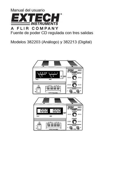
Manual del usuarioFuente de poder CD regulada con tres salidas Modelos 382203 (Análogo) y 382213 (Digital)IntroducciónFelicitaciones por seleccionar la Fuente de poder CD regulado Modelos 382203 (análogo) o 382213 (digital) de Extech. Los modelos 382203 y 382213 son fuentes de poder reguladas de estado sólido y compactos, apropiadas para muchas aplicaciones incluyendo pruebas de banco, servicio de campo, equipo de telecomunicaciones y diversión.Descripción del medidor1. Pantallas LCD Voltaje y Corriente2. LED indicador de estado de límite de corriente3. Interruptor de encendido con LED de estado4. Terminales de salida 5V y 12V fijo5. Terminales de salida alimentación variable6. Perillas de ajuste de voltaje y corriente variableNota: El Modelo 382213 (escalas LCD) se muestra arriba. El Modelo 382203 (mostrado en la portada) usa escala análoga.Operación1. La Fuente de poder debe ser alimentada con voltaje de línea nominal (110V ó 220V) dentro de+ 5%.2. Antes de encender, retire todas las cargas conectadas y fije la perilla de ajuste de voltajetotalmente contrarreloj (salida 0V CD).3. Para operar la fuente de alimentación como fuente de corriente constante, la salida de corrientedebe fijarse entre 10% y 100% del valor nominal (3A). El indicador de limitación de corriente se iluminará al activarse el circuito limitador de corriente.4. Use las perillas para ajuste de corriente y voltaje para fijar las salidas variables de corriente yvoltaje respectivamente. Use las terminales de salida variable para conexiones.5. Para las salidas de 5VCD y 12VCD, use las terminales de salida fija.6. Las pantallas análoga o digital indicaran las salidas reales de corriente y voltaje.7. Mantenga libre de obstrucciones las rejillas de ventilación del medidor (arriba y lados) paraprevenir sobrecalentamiento.Especificaciones382203382213Indicador Análogo doble conescalas Pantalla LCD doble de 3dígitosSalida de voltaje, CD0-30VSalida de corriente, CD0 - 3 amperiosIndicador de límite decorrienteLED de estadoPrecisión ± 7% de la escala total ± 1% de la escala total + 2dígitosOndulación y Ruido< 5mVRegulación de línea< 0,05% + 10mVVoltaje fijo de salida5V / 0,5A (Continuo); 1A (máx.)12V / 0,5A (Continuo); 1A (máx.)Tensión110/220VCA 50/60Hz (conmutable) Dimensiones152 x 142 x 242mm(6 x 5,6 x 9,5") (WxHxD)Peso4,5 kg (10 lbs.)Copyright (c)2012 Extech Instruments Corporation (a FLIR company) Reservados todos los derechos, incluyendo el derecho de reproducción total o parcial en cualquier medi o.。
Semi-synthetic aristolactams—inhibitors of CDK2enzymeVinod R.Hegde *,Scott Borges,Haiyan Pu,Mahesh Patel,Vincent P.Gullo,Bonnie Wu,Paul Kirschmeier,Michael J.Williams,Vincent Madison,Thierry Fischmann,Tze-Ming ChanSchering Plough Research Institute,2015Galloping Hill Road,Kenilworth,NJ 07033,USAa r t i c l e i n f o Article history:Received 7August 2009Revised 23December 2009Accepted 4January 2010Available online 7January 2010Keywords:Semi-synthetic analogs Aristolactams IC 50SARa b s t r a c tSeveral analogs of aristolochic acids were isolated and derivatized into their lactam derivatives to study their inhibition in CDK2assay.The study helped to derive some conclusions about the structure–activity relation around the phenanthrin moiety.Semi-synthetic aristolactam 21showed good activity with inhi-bition IC 50of 35nM in CDK2assay.The activity of this compound was comparable to some of the most potent synthetic compounds reported in the literature.Ó2010Elsevier Ltd.All rights reserved.In the preceding Letter we have reported on the isolation of a potent CDK2enzyme inhibitor SCH 546909,a natural product aris-tolactam analog with an inhibition IC 50of 140nM.This prompted us to undertake a semi-synthetic study of different analogs from this class.Many total syntheses of aristolactam analogs have been reported in the literature,1,2however sub-structure literature searches revealed that these compounds could be easily prepared from naturally occurring,aristolochic acids.HO H 3CONHOHOSCH 546909Several publications and reviews have been published on the occurrence,synthesis and biological activities of aristolochic acids.Aristolochic acids and aristolactams are classified as aporphinoids because of their basic skeleton which bears a distinct similarity to that of aporphins.Aristolochic acids exhibit tumor inhibitory activ-ity against the adenocarcinoma 755test system but in mice they induced papiloma.3They are also known to form covalent DNA adducts by enzymatic reductive activation of aristolochic acids in the presence of DNA.4They are also shown to induce mutagenicity in mice.5Aristolochic acid is commercially available from SigmaChemical Co.and ACROS.The commercially available aristolochic acid is a complex mixture of several analogs,with the major com-ponents being aristolochic acids II &I in 1:4ratio.We have sepa-rated commercial aristolochic acid mixtures on a preparative HPLC using YMC ODS-A C-18,10l m,5Â50cm HPLC column,eluting with 0.05%trifluoroacetic acid and acetonitrile (60:40)to obtain compounds 1–8.A typical 600mg of commercial aristolo-chic acid afforded 27.7,4.6,7.8,71.6,5.4,6.8,315.8,and 3.2mg of aristolochic acid C (5),6aristolochic D (7),77-hydroxy aristolo-chic A(6),8aristolochic acid II (1),aristolochic acid IV (4),97-meth-oxy aristolochic acid A (3),10aristolochic acid I (2),2and aristolochic acid III (8).11In our semi-synthetic modifications to prepare aristolactam analogs,the aristolochic acids were first converted to their lactams.The purified aristolochic acids were hydrogenated in ethanolic solution under 40psi hydrogen in presence of Pd/C catalyst,over-night at room temperature.The amino compound produced on reduction of nitro group,on further ring closure results in lactam.After separation and derivatization to the resulting lactam,the aromatic phenol ether derivatives were deprotected with BBr 3in methylene chloride solution.A typical demethylation 12involved stirring the aristolochic methyl ethers (15mg)in CH 2Cl 2(50ml)at 0°C with the dropwise addition of BBr 3(7.5ml,1M)in CH 2Cl 2at 0°C and then continue stirring overnight at room temperature.The reaction mixture was quenched in ice,extracted with ethyl acetate,and dried.The demethylated product was purified by HPLC.The Methylenedioxy group was removed by stirring aristolac-tams in CH 2Cl 2at 0°C and dropwise addition of a solution of PCl 5(1:1ratio).The reaction mixture was slowly allowed to attain room0960-894X/$-see front matter Ó2010Elsevier Ltd.All rights reserved.doi:10.1016/j.bmcl.2010.01.007*Corresponding author.Tel.:+19088203871;fax:+19088206166.E-mail address:**********************(V.R.Hegde).Bioorganic &Medicinal Chemistry Letters 20(2010)1384–1387Contents lists available at ScienceDirectBioorganic &Medicinal Chemistry Lettersj o ur na l h om e pa ge :w w w.e lse v ie r.c om /lo c at e/bm c ltemperature during2h and then quenched with ice,extracted with CH2Cl2and dried.The O-dihydroxy compound formed was purified by HPLC.3,4-Dihydroxy-12-chloro aristolactams were prepared from methylenedioxy containing derivatives via treatment with the dropwise addition of PCl5(1:2.5ratio)in CH2Cl2at0°C and slowly allowing the reaction mixture to attain room temperature during 3h.The reaction mixture was quenched in ice,extracted with CH2Cl2and dried.The halogenated product was further purified by HPLC.O OCOOHNO2OONR1R2R31. R1 = R2 = R3 = -H2. R1 = -OCH3, R2 = R3 = -H3. R1 = R2 = -OCH3, R3 = -H4. R1 = R3 = -OCH3, R2 = -H5.R1 = R2 = -H, R3 = -OH6. R1 = -OCH3, R2 = -OH, R3 = -H7. R1 = -OCH3, R2 = -H, R3 = -OH8. R1 = -OH,R2 = R3 = -H9. R1 = R2 = -OCH3, R3 = -HOR1R2R3R4R515. R1 = R2 = R3 = R4 = R5 =-H16. R1 = -OCH3, R2 = R3 = R4 =R5 = -H17. R1 = R2 =-OCH3 ,R3 =R4 = R5 = -H18. R1 = R3 = -OCH3, R2 = R4 = R5 = -H19. R1 = -OCH3, R2 = -OH, R3 = R4 =R5 = -H20. R1 = -OCH3, R3 = -OH, R2 = R4 = R5 = -H21. R1 = -OH, R2 = R3 = R4 = R5 = -H22. R1 = R2 = -OH, R3 = R4 = R5 = -H23. R1 = R3 = -OH, R2 = R4 = R5 = -H24. R1 = R2 = R4 = R5 = -H, R3 = -OH,25. R1 = -OCH3, R2 = R3 = R4 = -H, R5 = -CH326. R1 = -OH, R2 = R3 = R4 = -H, R5 = -CH3ARISTOLOCHIC ACID ANALOGSHO HOCOOHNO2R4R1R2R310. R1 = R2 = R3 = R4 = -H11. R1 = R2 = R3 = -H, R4 = -Cl12. R1 = -OCH3, R2 = R3 = R4 = -H13. R1 = -OH, R2 = R3 = R4 = -H14. R1 = -OCH3, R2 = R3 = -H, R4 = -Cl 27. R1 = R2 = R3 = R4 = -H28. R1 = R2 = R3 = -H, R4 = -Cl29. R1 = -OCH3, R2 = R3 = R4 = -H30. R1 = -OH, R2 = R3 = R4 = -H31. R1 = -OCH3,R2 =R3 = -H, R4 = -ClHOHONHOR4R1R2R3The aristolochic acid analogs prepared were tested in CDK2as-say13with the resulting inhibition IC50s are tabulated in Table1. Many analogs showed CDK2activity>10l M,however compounds 13,16,19,21,and24exhibited CDK2inhibition under10l M. Compound21showed a CDK2inhibition IC50of35nM,potency similar to the most potent CDK2inhibitor reported in the litera-ture14Compound13,having a hydroxyl group at C-9also showed activity in the l M range.Several natural products,like aporphinoids,morphine,and fused berberine classes of compounds,were also tested to evaluate importance of the lactam ring in the CDK2activity.All these com-pounds excepting sinomenine,sinoacutine,and tetrahydroberber-ine,have tetrahydro pyridine ring attached to phenanthrine moiety.Sinomenine and sinoacutine have morphine like ring sys-tem but tetrahydroberberine has two tetrahydro-isoquinoline ring system.All these compounds failed to show inhibition in CDK2as-say at50l M.Only compound21,displayed strong CDK2inhibition,about threefold better than the natural product SCH546909.Based on the activity profile of the different aristolochic acid and aristolactam analogs,it appears the lactam ring is essential for potent CDK2inhibition.This has been shown to be true for sev-eral potent inhibitors reported in literature.31,32Hydroxyl groups at C-7or C-9positions also appear to enhance CDK2inhibition. Additionally,theprotection of the dihydroxy groups atthe C-4 and C-5positions contributes toward the potency.However,pro-tection of amide–NH by a methyl group or substitution by a halo-gen at C-10results in reduced activity.The observations are only empirical and a detailed study would be necessary to evaluate a complete structure–activity relationship.Protection increasesthe potency in CDK2assay-CH3 in this positiondecreases activityhalogen in this positiondecrease in potencyincreases the potencyAristolochic acids and aristolactams have phenanthrin aromatic moiety similar to another class of natural product that includes staurosporine,isolated from fungus.Staurosporins are also potent kinase inhibitors and have been extensively studied as antitumor compounds.Like staurosporine,these compounds are also planar molecules and are sparingly soluble in various solvents including water.Increasing the solubility properties by salt formation or by Table1CDK2inhibition IC50s of aristolochic acids and aristolactam analogs Compound CDK2IC50(l M)1>202>203>204>205306257258159>201013.4111812>3013 5.71416.51516151616 1.217>151815>1519 2.92018>3521180.03522>302318>502420,21 2.152519,21>352617>35274>3528>2529>353016>353110Dicentrine22>50Crebanine23>50Roemerine-HBr24>50Isocorydine25>50Corydine26>50Corytuberine27>50Sinoacutine28>50Sinomenine29>50Stephanine,25>50Tetrahydro-berberine30>50V.R.Hegde et al./Bioorg.Med.Chem.Lett.20(2010)1384–13871385forming inclusion compounds with b -cyclodextrin appear to improve cellular activity.Aristolactam 21was further tested in a kinase counter screen assays,along with the natural product SCH 546909and 3233,as shown in Table 2.The results indicate that the inhibitors share a similar activity in the CDC2(cyclin-A dependent kinase,$90%homology)assay,and a lesser selectivity in other kinases assays like CDK4,AUR2(Aurora kinase),MAPK (mitogen-activated protein kinase),and AKT (ATP kinase).Cellular activities:Compound 21,the most potent and selective CDK2inhibitor from this series,was evaluated in two cellular pro-liferation assays:a colony forming assay and a soft agar growth as-say.In the soft agar growth assay compound 21showed comparable activity to 32,although compound 32appeared to lose some potency in this assay format compared to the clonogenicity assay (Table 2).In the clonogenicity assay using MCF-7cells,all three compounds inhibited growth at similar micromolar pound 21inhibited proliferation of tumor cells,with IC 50values consistent with CDK2inhibitors that are competitive with respect to ATP.The anti-proliferative activity of the com-pounds was up to eightfold selective for the tumor cells relative to the HFF normal cell line.The anti-proliferative activity of 21ar-rests the tumor cells and protects the normal cells from chemo-therapy-induced toxicity.32These data are consistent with an anti-proliferative mechanism expected for inhibition of CDK2and revealed that the aristolactam class of compounds have potential for treating proliferative disorders,including chemotherapy-in-duced alopecia.NN HNORPyrazoloquinolines32. R = -OCH 3 (SCH47089)Computer based interaction design of 21with CDK2enzyme:Thedocking experiments on CDK2enzyme with 21(SCH535270)and staurosporine were performed and are shown in Figure 1A and B.The computer docking model suggests the lactam of 21(SCH 535270)interacts with CDK2enzyme active sites in a manner anal-ogous to that observed for compounds of staurosporine class of inhibitors bound to fibroblast growth factor receptor kinase.34Two hydrogen bonds were formed between the c -lactam moi-ety of 21and CDK2.Specifically,the amide nitrogen was hydrogen bonded to the backbone carbonyl of glu-81of the CDK2enzyme and the lactam carbonyl oxygen was hydrogen bonded with the backbone NH of leu-83amide.Staurosporin also binds to the CDK2enzyme in a similar fashion.The C-9hydroxy group also ap-pears to stabilize the binding at some other sight of enzyme core.35SCH 535270,like staurosporin,is a planar molecule and exhibits similar biological properties.X-ray crystallography:Our attempts to determine the X-ray structure of inhibitor SCH 535270bound to CDK2have failed.The crystals were prepared by soaking the compound in presence of CDK2enzyme and cyclin A.The parameters like compound concentration and duration of soak were screened.Examination of the electronic density maps did not reveal the binding mode of the compound.In some cases,X-ray crystallogra-phy has failed to determine the co-structures of a compound bound to the CDK2protein even in the case of potent inhibitors.A possible explanation is that inhibitor binding requires the com-plete CDK2-cyclin-A complex,which is protocol in our screening assay.CDK2is activated by complexing with cyclin-A that induces conformational changes in the protein that affect the ATP binding site to some degree.The most significant effect involves a rotation of the C-helix,which alters the active-site geometry in the region of the triad of catalytic active-site residues Lys-33,Glu-51,and Asp-145.The amino group of Lys-33can be potential interaction site for inhibitors.The amino nitrogen appears to hydrogen bond with the oxygen of methylenedioxy group.Efforts to grow crystalsTable 2Inhibition (IC 50)of SCH 546909,21and 32in different kinases CompoundActivity IC 50(nM)Selectivity (nM)Cellular activity (l M)CDC2CDK4AUR2MAPK AKT SAG MCF7Clonogenicity SCH5469091402141420214035,335———32(SCH47089)2020020005000>50,000—>10 3.021(SCH535270)352009000350012,00011,4002–2.53.5Figure puter modeling of binding of 21(SCH 535270)and staurosporin with CDK2enzyme.1386V.R.Hegde et al./Bioorg.Med.Chem.Lett.20(2010)1384–1387of the activated CDK2-cyclin-A protein complex are in progress and will be reported in future publications.The aristolactam class of compounds represents a novel class of CDK2inhibitors.Exploration into semi-synthetic analogs provided a potent CDK2inhibitor from this class.Binding interactions by docking experiments suggested carbonyl of glu-81and NH of leu-83amide of the CDK2enzyme are involved in hydrogen bond-ing with the lactam functionality of aristolactams.CDK2inhibition causes an arrest of the cell cycle and exhibits a selective killing effect on several tumor cell lines.36AcknowledgmentsAuthors gracefully acknowledge Dr.E.Lees and Dr.R.Doll for their helpful discussion on CDK2inhibitors.References and notes1.Mix,D.B.;Guinaudeau,H.;Shamma,M.J.Nat.Prod.1982,45,657.2.Shamma,M.;Monit,J.C.Isoquinoline Alkaloids Research1972–1977;PlenumPress:New York,1978.3.(a)Kupchan,S.M.;Wormser,.Chem.1965,30,3792;(b)Kupchan,S.M.;Merianos,.Chem.1968,33,3735.4.(a)Stiborova,M.;Frei,E.;Breuer,C.A.;Schmeiser,H.H.Cancer Res.1990,50,5464;(b)Cinca,S.;Voiculetz,N.;Schmeiser,H.;Wiessler,M.J.Med.Biochem.1997,1,3.5.Pistelli,L.;Nieri,E.;Bilia,A.R.;Marsili,A.;Scarpato,R.J.Nat.Prod.1993,56,1605.6.Hong,L.;Sakagami,Y.;Marumo,S.;Xinmin,C.Phytochemistry1994,37,237.7.Nakanishi,T.;Iwasaki,K.;Nasu,M.;Miura,I.;Yoneda,K.Phytochemistry1982,21,1759.8.Wu,T.-S.;Leu,Y.-L.;Chan,Y.-Y.Chem.Pham.Bull.1999,47,571.9.De Pascual,T.J.;Urones,J.G.;Fernandez,A.Phytochemistry1983,22,2745.10.Wu,T.-S.;Chan,Y.-Y.;Leu,Y.-L.Chem.Pharm.Bull.2000,48.11.Urzua,A.;Salgado,G.;Cassels,B.K.;Eckhardt,G.Planta Med.1982,45,51.12.Gerecke,M.;Borer,R.;Brossi,A.Helv.Chim.Acta1976,59,2551.13.Guzi,T.J.;Paruch,K.;Dwyer,M.P.;Doll,R.J.;Girijavallabhan,V.M.;Mallams,A.;Alvarez, C.S.;Keertikar,K.M.;Rivera,J.;Chan,T.-Y.;Madison,V.S.;Fischmann,T.O.;Dillard,L.W.;Tran,V.D.;He,Z.;James,R.A.;Park,H.;Paradkar,V.M.;Hobbs,D.W.;Kirschmeier,P.;Bannerji,R.U.S.Patent Appl.Publ.2008,pp.387.14.(a)Babu,P.A.;Narasu,M.L.;Srinivas,K.ARKIVOC2007,2,247(Gainesville,FL,USA);(b)Ruetz,S.;Fabbro,D.;Zimmermann,J.;Meyer,T.;Gray,N.Curr.Med.Chem.:Anti-Cancer Agents2003,3,1;(c)Dumas,J.Exp.Opin.Ther.Patents2001, 11,405.15.Priestap,H.Phytochemistry1985,24,849.16.Coutts,R.T.;Stenlake,J.B.;Williams,W.D.J.Chem.Soc.1957,4120.17.Chakraborty,S.;Nandi,R.;Maiti,M.;Achari,B.;Bandyopadhyay,S.Photochem.Photobiol.1989,50,685.18.Eckhardt,G.;Urzua,A.;Cassels,B.K.J.Nat.Prod.1983,46,92–97.19.Achari,B.;Bandyopadhyay,S.;Chakravarty,A.K.;Pakrashi,.Magn.Reson.1984,22,741.20.Mizuno,M.;Oka,M.;Tanaka,T.;Yamamoto,H.;Iinuma,M.;Murata,H.Chem.Pharm.Bull.1991,39,1310.21.(a)Chakraborty,S.;Nandi,R.;Maiti,M.;Sur,P.Indian J.Phys.B.1991,65B,587;(b)Priestap,H.A.Magn.Reson.Chem.1989,27,460.22.Chen,C.C.;Huang,Y.L.;Ou,J.C.;Su,M.J.;Yu,S.M.;Teng,C.M.Planta Med.1991,57,406.23.Shamma,M.;Slusarchyk,W.A.Chem.Rev.1964,64,59.24.You,M.;Wickramaratne, D. B.;Silva,G.L.;Chai,H.;Chagwedera,T. E.;Farnsworth,N.R.;Cordell,G.A.;Kinghorn,A.D.;Pezzuto,J.M.J.Nat.Prod.1995,58,598.25.Roblot,F.;Hocquemiller,R.;Cave,A.;Moretti,C.J.Nat.Prod.1983,46,862.26.Manske,R.H.F.Can.J.Res.1932,7,258.27.Wang,C.-C.;Kuoh,C.-S.;Wu,T.-S.J.Nat.Prod.1996,59,409.28.Kunitomo,J.;Ju-Ichi,M.;Yoshikawa,Y.;Chikamatsu,H.J.Pharm.Soc.Jpn.1974,94,97.29.Terui,Y.;Tori,K.;Maeda,S.;Sawa,Y.K.Tetrahedron Lett.1975,33,2853.30.Chen,C.Y.;MacLean,D.B.Can.J.Chem.1968,46,2501.31.Dumas,J.Exp.Opin.Ther.Patents2000,11,405.32.Davis,S.T.;Benson,B.G.;Bramson,H.N.;Chapman,D.E.;Dickerson,S.H.Science2001,291,134.33.Afonso,A.;Kelly,J.M.;Chackalamannil,S.U.S.Patent5459146,1995,pp13.34.Mohammadi,M.;McMahon,G.;Sun,L.;Tang,C.;Hirth,P.Science1997,276,955.35.Bramson,H.N.;Corona,J.;Davis,S.T.;Dickerson,S.H.;Edelstein,M.;Frye,S.V.,;Gampe,R.T.,Jr.;Harris,P.A.;Hassell,A.;Holmes,W.D.;Hunter,R.N.;Lackey,K.E.;Lovejoy,B.;Luzzio,M.J.;Montana,V.;Rocque,W.J.;Rusnak,R.D.;Shewchuk,L.;Veal,J.M.;Walker,D.H.;Kuyper,L.F.J.Med.Chem.2001,44, 4339.36.Walker,D.H.;Luzzio,M.;Veal,J.;Dold,K.;Edelstein,M.Proc.Am.Assoc.CancerRes.1999,40,A4783Physico-chemical properties:Aristolochic acid C(5):UV k max:225,256,308,410nm;FABMS328(M+H)+,350 (M+Na)+,366(M+K)+,1H NMR(DMSO-d6)d:10.63(COO H),8.48(9-H),8.46(d, J=4Hz,5-H),8.10(d,J=17Hz,8-H),7.75(s,2H),7.29(dd,J=17,4Hz,7-H),6.48(s,12-H2).13C NMR(DMSO-d6)ppm:168.0(11-C),159.8(6-C),145.8(3-C),145.5(4-C),143.1(10-C),132.5(8-C),131.0(4b-C),126.4(9-C),123.7(1-C),121.5(8a-C),118.8(7-C),117.2(10a-C),116.2(4a-C),111.9(2-C),111.1(5-C), 102.8(12-C).7-Hydroxy aristolochic acid A(6):UV k max:224,271,318,384nm;ESMSÀve mode,m/z356(MÀH)À.Aristolochic acid D(7):UV k max:224,243,333,408nm;ESMS m/z358(M+H)+.Compound(21)18:UV k max:214,242,258,294,328,398nm;ESMS:m/z280 (M+H)+;1H NMR(DMSO-d6)d:10.72(s,NH),10.2(s,–OH),8.03(d,J=15Hz,5-H),7.63(s,2-H),7.37(t,J=15Hz,6-H),7.36(s,9-H),7.06(d,J=15Hz,7-H),6.46(s,12-H2).13C NMR(DMSO-d6)ppm:168.1(11-C),153.8(8-C),148.8(3-C),147.1(4-C),134.0(10-C),125.8(6-C),125.3(4b-C),125.3(10a-C),123.2(8a-C),119.3(1-C),117.5(5-C),112.3(7-C),111.3(4a-C),105.4(2-C),103.2 (12-C),98.7(9-C).Compound(16)16:UV k max:225,239,258,295,329,394nm;ESMS:m/z294 (M+H)+;1H NMR(DMSO-d6)d:10.67(s,NH),8.22(d,J=16Hz,5-H),7.70(s,2-H),7.50(t,J=16Hz,6-H),7.35(s,9-H),7.20(d,J=16Hz,7-H),6.48(s,12-H2),4.0(s,13-H3).13C NMR(DMSO-d6)ppm:168.1(11-C),155.3(8-C),148.8(3-C),147.1(4-C),134.7(10-C),125.7(6-C),125.0(11a-C),124.8(4b-C),124.0(10a-C),119.3(1-C),118.7(5-C),111.0(4a-C),108.3(7-C),105.7(2-H),103.3(12-C),97.9(9-C)add–OCH3value.Compound(29):ESMS:m/z316(M+H)+;1H NMR(DMSO-d6)d:9.12(d, J=16Hz,5-H),7.52(t,J=16Hz,6-H),7.50(s,2-H),7.22(d,J=16Hz,7-H),3.92 (s,–OCH3),13C NMR(DMSO-d6)ppm:NOE from–OCH3to proton doublet at d7.22due to7-H and no NOE from–OCH3.All the new compounds were purified by HPLC and identified by MS.V.R.Hegde et al./Bioorg.Med.Chem.Lett.20(2010)1384–13871387。
芝奇推出TridentZNeo焰光戟DDR4-3800套装,时序只有
惊人的CL14
芝奇在上个月AMD发布第三代锐龙处理器的时候同步推出了Trident Z Neo焰光戟内存,这套内存是专门为Ryzen 3000系列处理器及X570平台所打造的,不过首发的时候内存频率只能到3600MHz,实际上AMD Zen 2架构的内存最佳分频频率是3800MHz,在这个频率能够获得最低的内存延迟,现在芝奇就推出了焰光戟DDR4-3800的套装,而且时序还可以维持在CL14的低水平。
焰光戟内存延续的幻光戟的大体设计,顶部的导光带就是幻光戟那种设计,散热片是三叉戟系列的,但是表面使用了两种设计,一半是磨砂质感的冰晶银,而另一半是细致发丝的雅典黑,衬托其优雅不凡的高科技质感。
芝奇Trident Z Neo焰光戟内存现在新增了DDR4-3800 8GB*2和8GB*4的套装,此套装采用严选高效能三星B-Die颗粒,时序可以维持在CL14-16-16-36的超低水平,CL14的3800MHz可是相当罕见的,下图为此规格搭配AMD Ryzen 9 3900X CPU 及微星MEG X570 GODLIKE主板,在Infinity Fabric运作频率与内存频率为1:1的情况下,AIDA64 的测试中读写高达58114MB/s及56064 MB/s的惊人速度,延迟也只有66.3ns。
此DDR4-3800 CL14-16-16-36终极套装已通过芝奇内部严谨的测试验证,确保绝佳稳定性,以下图分别为32GB套装搭配华硕ROG CROSSHAIR VIII Formula主板和AMD Ryzen 5 3600X CPU通过烧机测试截图,从图上我们可以看到这套内存的工作电压高达1.5V:。
1Connect the power adapter and press the power buttonConecte el adaptador de alimentación y presione el botón de encendido Sambungkan adaptor daya dan tekan tombol daya.ليغشتلا رز ىلع طغضلاو رايتلا ئياهم ليصوتب مقProduct support and manuals Manuales y soporte del producto Dukungan dan panduan produkةلدلأاو جتنملا معد/support/support/manuals /support/windowsContact DellPóngase en contacto con Dell | Hubungi DellDell ـب لاصتلاا/contactdellRegulatory and safetyInformación reglamentaria y de seguridadRegulasi dan keselamatan | ةيميظنتلا تاسرامملاو ناملأا تاسرامم/regulatory_complianceRegulatory modelModelo reglamentario | Model regulatoriيميظنتلا ليدوملاP27SRegulatory typeTipo reglamentario | Jenis regulatori Regulatory type | يميظنتلا عونلاP27S002Computer modelModelo del equipo | Model komputerرتويبمكلا زاهج زارطLatitude 52902017-11What’s NewNovedades | Apa yang Baruةديدجلا تازيملا• Supports Dual (7th Gen Intel ® Core ™) and Quad (8th Gen Intel Core) processors• Supports up to 2400 MHz DDR4 memory with 8th Gen Intel Core processors• Compatibilidad con procesadores dobles (Intel ® Core ™ de 7.a generación) y procesadores cuádruples (Intel Core de 8.a generación)• Compatibilidad con memoria DDR4 de hasta 2400 MHz con procesadores Intel Core de 8.a generación• Mendukung prosesor Dual (Intel ® Core ™ Generasi Ke-7) dan Quad (Intel Core Generasi Ke-8)• Mendukung hingga 2400 MHz memori DDR4 dengan prosesor Intel Core Generasi Ke-8ةاونلا ةيعابرو )عباسلا ليجلا نم Intel ® Core ™ ( ةاونلا ةيئانث تاجلاعملا معدي)نماثلا ليجلا نم Intel Core (نم Intel Core تاجلاعم عم زترهاجيم 2400 ىلإ لصت ةعرسب DDR4 ةركاذ معد نماثلا ليجلاDi impor oleh:PT Dell IndonesiaMenara BCA Lantai 48 Unit 4804Jalan M.H Thamrin No. 1 Jakarta Pusat,10310 Indonesia© 2017 Dell Inc. or its subsidiaries.© 2017 Intel Corporation.Features Características | Fitur |تازيملا1. Cámara2. Indicador luminoso de estado de lacámara3. Ranura para tarjeta microSIM(opcional)4. Lectora de tarjetas micro-SD5. Emisor de infrarrojos (opcional)6. Cámara de infrarrojos (opcional)7. Cámara (opcional)8. Indicador luminoso de estado de lacámara (opcional)9. Micrófonos de arreglo doble10. Indicador LED de botón de encendido/estado de alimentación11. Ranura para cierre de seguridad Noble12. Puerto de red13. Puerto VGA14. Puerto USB 3.1 de primera generacióncon PowerShare15. Puerto para auriculares y micrófono16. Lectora táctil de huellas dactilares(opcional)17. Indicador luminoso de estado de cargade la batería18. Sensor NFC (opcional)19. Superficie táctil20. Altavoces21. Lector de tarjetas inteligentes(opcional)22. Puerto USB 3.1 Gen 123. Puerto HDMI24. DisplayPort por USB Tipo C25. Puerto del conector de alimentación26. Indicador luminoso de estado delmicrófono27. Etiqueta de servicio1. Kamera2. Lampu status kamera3. Slot kartu SIM mikro (opsional)4. Satu pembaca kartu microSD5. Pemancar inframerah (IR) (opsional)6. Kamera inframerah (opsional)7. Kamera (opsional)8. Lampu status kamera (opsional)9. Rangkaian Mikrofon Ganda10. Tombol daya/LED status daya11. Slot kunci Nobel Wedge12. Port jaringan13. Port VGA14. Port USB 3.1 Tdengan PowerShare15. Port Headset/Microphone16. Pembaca sidik jari sentuhan(opsional)17. Lampu status pengisian baterai18. Sensor NFC (opsional)19. Panel sentuh20. Speaker21. Pembaca kartu pintar (opsional)22. Port USB 3.1 Gen 123. Port HDMI24. DisplayPort di atas USB Tipe-C25. Port konektor daya26. Lampu status mikrofon27. Label Tag Servis15. Headset/Microphone port16. Touch Fingerprint reader (optional)17. Battery charge status light18. NFC sensor (optional)19. Touchpad20. Speakers21. Smartcard reader (optional)22. USB 3.1 Gen 1 port23. HDMI port24. DisplayPort over USB Type-C25. Power connector port26. Microphone status light27. Service Tag label1.اريماكلا2.اريماكلا ةلاح حابصم3.)ةيرايتخا( micro-SIM ةقاطب ةحتف4.microSD تاقاطب ئراق5.)IR( ءارمحلا تحت ةعشلأا ثب زاهج)يرايتخا(6.ءارمحلا تحت ةعشلأاب ةلماعلا اريماكلا)يرايتخا(7.)ةيرايتخا( اريماكلا8.)يرايتخا( اريماكلا ةلاح حابصم9.ةيئانثلا فيفصلا تانوفوركيم10.ةلاح نايبل LED حابصم/ليغشتلا رزةقاطلا11.Nobel Wedge لفق ةحتف12.ةكبشلا ذفنم13.VGA ذفنم14.دوزم لولأا ليجلا نم USB 3.1 ذفنمPowerShare ةزيمب15.نوفوركيملا/سأرلا ةعامس ذفنم16.سمللاب لمعي يذلا عبصلإا ةمصب ئراق)يرايتخا(17.ةيراطبلا نحش ةلاح حابصم18.)يرايتخا( NFC رعشتسم19.سمللا ةحول20.توصلا تاربكم21.)يرايتخا( Smartcard ئراق22.لولأا ليجلا نم USB 3.1 ذفنم23.HDMI ذفنم24.نم USB ربع DisplayPort ذفنمC عونلا25.رايتلا لصوم ذفنم26.نوفوركيملا ةلاح حابصم27.ةمدخلا زمر قصلم。
E v a l u a t i o nC e r t i f i c a t e Issuing Aut horit y NM i Certin B.V.22 December 2016C. Oost ermanHead C ert ificat ion BoardNM i Certin B.V. Hugo de Groot plein 1 3314 EG Dordrecht The Net herlandsT +31 78 6332332 cert in@nmi.nlwww.nmi.nl This document is iss ued under t he provis ion t hatno liability is accept ed and that the applicants hall indemnify third-part y liabilit y.R eproduction of t he completedocument only is permitt ed.Number TC10822 revision 0Project number: 16200475Page 1 of 1Issued by NM i C ert in B.V.In accordance w it h Aspect s of t he Volunt aryOIM L R117-Producer Endress + Hauser Flow t ec AGKägenst rasse 7C H-4153 ReinachS w it zerlandM easuring inst rument A flow transm itt er (calculat ing/indicat ing device for Endress + HauserC oriolis meters), int ended t o be used as a part of a measuring inst rument.Brand : Endress + Hauser Flow t ec AGDesignat ion : Promass 300S oft w are versions : see paragraph 1.2 of t he descript ionAccuracy class : 0,3Environment classes : M3 / E2Temperat ure range ambient: -40 °C +55 °CFurt her propert ies and t est result s are described in t he annexes:Descript ion TC10822 revision 0;Document at ion folder TC10822-1.R emarks An overview of t he performed t est s is given in Annex 2 appert aining t ot his Evaluat ion Cert ificat e.Number TC10822 revision 0Project number 16200475Page 1 of 51General inform ation on the flow transm itterAll propert ies of t his flow t ransmit t er, w het her ment ioned or not, shall not be in conflictw it h t he Legislat ion.This Evaluat ion Cert ificat e is t he posit ive result of t he applied volunt ary, modular approach, for a component of a measuring inst rument, as described in WELM EC guide 8.8.The complet e measuring inst rument must be covered by an EC-t ype examinat ion C ert ificat e or an EU-t ype examinat ion C ert ificat e.This Evaluat ion Cert ificat e is valid for t he Endress + Hauser flow t ransmit t er, as described in paragraph 1.1 of t he descript ion and may only be used in combinat ion w it h Coriolismeasurement sensors manufact ured by Endress + Hauser Flow t ec AG:- That are covered by an Evaluat ion Cert ificate;- Direct ly ment ioned in t he EU-t ype examinat ion cert ificat e of t he measuring syst em.1.1Essential PartsDescript ion Docum ent at ionRem arksnum berPow er Supply100 240 V AC / 50/60 Hz 10822/0-02; 10822/0-0324 V DC 10822/0-04; 10822/0-05100 240 V AC / 50/60 Hz;10822/0-06; 10822/0-0724 V DCA m plif ierFor Exi Hart10822/0-08; 10822/0-09 Zone 1 st andardFor Exi Hart10822/0-10; 10822/0-11 Zone 1 IIC 200 °CFor M odbus and Hart10822/0-12; 10822/0-13 Zone 2For Exd M odbus and Hart10822/0-14; 10822/0-15 Zone 1 st andardFor Exd M odbus and Hart10822/0-16; 10822/0-17 Zone 1 IIC 200 °CCPU M odemFor Exi hart devices 10822/0-18; 10822/0-19 I/O 1 = Exi current out put + HartFor Non-Ex Hart devices 10822/0-20; 10822/0-21 I/O 1 = C urrent out put + HartFor M odbus devices 10822/0-22; 10822/0-23 I/O 1 = M odbusI/O M odulesM ult i I/O module Non-Ex 10822/0-24; 10822/0-25 Frequency, pulse, st at us in/out,current in/outM ult i I/O module Ex 10822/0-26; 10822/0-27Double pulse 10822/0-28; 10822/0-29 Double pulse channel, phaseshift edDisplayDisplay module 10822/0-30; 10822/0-31 Int egrat ed in flow t ransmit t er orremot e (ext ernal) moduleNumber TC10822 revision 0Project number 16200475Page 2 of 5Descript ion Docum ent at ionRem arksnum berTerm inal boardsTerminal board 10822/0-32; 10822/0-33 For Ex devicesTerminal board 10822/0-34; 10822/0-35 For Non-Ex devicesTerminal board 10822/0-36 Used at remot e display moduleBack planeFor Ex devices 10822/0-37; 10822/0-38For non Ex devices 10822/0-39; 10822/0-40- Input s (sensor side)From t he connect ed C oriolis sensor t he Promass 300 receives:Tw o pick-of f signals; analogue mV signals from w hich t he mass flow and densit y aredeterminedOne t w o-w ire Pt-1000 t emperat ure t ransmit t er for t he measurement of t he t ubet emperat ureOne t w o-w ire Pt-1000 t emperat ure t ransmit t er for t he measurement of t he carriert ube t emperat ure.Please not e t hat t hese t emperat ures shall not be used for Cust ody Transfer relat edpurposes, but only for t he correct ion given above.- Out put s (sensor side)The Promass 300vibrat ing mot ion. The frequency of t he vibrat ion is aut omat ically adjust ed t o t heresonant f requency of t he measurement t ubes. This out put is referred t o as: drive current out put- Input/Out put (elect ronic calculat or/indicat ing device)The Promass 300 is equipped w it h t he follow ing C ust ody Transfer out put s: Double, 90° or 180° phase shif t ed pulse-out put for t he t ransmission of volume- ormass-informat ion. Phase shif t is select able4 20 mA out put for t he t ransmission of densit y. This out put can also be used forinput/out put via Hart prot ocol.Ot her informat ion can also be t ransmit t ed via t his out put (for example flow rat e), but t his informat ion is not W&M approved.4 20 mA input for t he t ransmission of product t emperat ure. The (ext ernal)t emperat ure is used for aut omat ic correct ion of t he t emperat ure influence on t heconnect ed measurement sensor and overrides bot h int ernal t w o-w ire Pt-1000t emperat ure sensors.4 20 mA input for t he t ransmission of product pressure. The pressure is used foraut omat ic correct ion of t he pressure influence on t he connect ed measurement sensor.S t at us input or st at us out put (depending on version)M odbus R S485 serial prot ocol. Dat a t ransmission is saf e guarded w it h C R C checksumover t he dat a package.Number TC10822 revision 0Project number 16200475Page 3 of 51.2Essential Characteristics-S oft w are t ype P;R isk C lass C;Ext ensions T and I-5 apply.- S oft w are-versionsVersion num bers Checksum01.00.02 0xE87F (M odbus)0x321F (Hart)The soft w are version and checksum can be verified on screen:S oft w are version, menus Diagnost ics Device Info Firmw are VersionC hecksum, menus Operat ion C ust ody Transfer ChecksumNot e t he s oft w are version includes t he soft w are of all modules ment ioned inparagraph 1.1.- C ust ody Transf er paramet ersThe C ust ody Transfer paramet ers and t he mandat ory set t ings are ment ioned in Annex 1.For securing t he Weight s and M easures paramet ers:Go t o menu S et up Advanced set up C ust.t rans. act.Login w it h aut horized user login and passw ord and complet e all ot her set t ings (dat eand t ime)S et dipsw it ch number 2 t o ON. Only t he Weight s and M easures paramet ers aresecured against changing.Aft er exit ing t he menu syst em, t he lock symbol () is show n on t he display and t hebot t om row show s t he Weight s and M easures count er.Alt ernat ive met hod is t o set dipsw itch number 1 to ON; t his secures all paramet ersagainst changing. The lock symbol () is show n on t he display.S ecurit y disabled S ecurit y enabled (paramet ers prot ect ed) - The flow t ransmit t er may only be used in combinat ion w it h an approved flow comput er[1] as t he display may not be used as a primary indicat ion.[1]The flow comput er must have an Evaluat ion or Part s Cert ificat e issued by a recognised Not ifiedBody under Annex M I-005 (M ID 2004/22/EC) or Annex VII (M ID 2014/32/EU).Number TC10822 revision 0 Project number 16200475 Page 4 of 51.3 Essential Shapes- Inscript ions of the Promass 300AtTC10822 is placed on t he housing(s) of the Promass 300; Ident ificat ion of t he measurementsensor; Serial number;In case of a remot e version: t he serial number of t he measurement sensor is inscribed on t he Promass 300 and/or t he serial number of t he Promass 300 is inscribed on t he measurement sensor. - S t at us of t he deviceIn case an elect ronic calculat or/indicat ing device is connect ed t o t he Promass 300, theis sent t o t he connect ed device in one of t he follow ing ways:-channels, t hus enabling t he flow comput er t o det ect a pulse failure and consequent ly generat e an alarm. Ifnecessary, an ext ra elect rical board is added t o prevent t his act ion short -circuit ing t hePromass 300.The current out put is set t o failure current (minimum or maximum value is possible), t hus enabling t he flow comput er t o det ect the failure.The Promass' pulse out put is set t o maximum pulse rat e for one channel and t o no pulses for t he ot her pulse channel. This w ill t rigger t he pulse securit y checking of t he connect ed elect ronic calculat or/ indicating device.The M odbus.In all cases t he st at us of t he device must be configured so, t hat t he alarm conditions- S ealing.S ee chapt er 2.- C ablingAll cables shall be shielded and t he shielding shall be connect ed on bot h sides.1.4 Conditional Part s- Key-boardThe keyboard consist s of a t hree keys of w hich t heir funct ion depends on t he menu and select ed it em. The keyboard is part of the LC D display. If t he display is not present , t he keyboard is also not present. - HousingInside t he met al housing t he Promass, t he essent ial and t he condit ional part s are mount ed. Access can be obt ained t hrough t w o sealable lids.S ee document at ion number 10822/0-01 for t he assembly of t he part s inside the housing. compact , explosion proof , direct ly mount ed on t he measurement sensor.Opt ionally t he display is mount ed in a separat e housing. The communicat ion w it h t he display is via M odbus.1.5 Conditional Shapes- Blinding of Promass displayIf an elect ronic calculat or/indicat ing device (flow comput er) is connect ed t o t he Promass 300, t he display (w hen present ) of t he Promass 300 may be blinded. The display is st ill pres ent and funct ioning, it is not possible t o read t he display.Number TC10822 revision 0Project number 16200475Page 5 of 52SealsAft er set t ing t he securit y sw it ch in t he secured posit ion, all lids are sealed against opening.3Conditions for Approval- Verify t he paramet ers set t ings ment ioned in Annex 1 for correct set t ing and w here applicable if t he set t ing is in accordance w it h t he calibrat ion dat a.- Ot her part ies may use t his Evaluat ion Cert ificat e only w it h t he w rit t en permission of Endress + Hauser Flow t ec AG, Kägenst rasse 7, CH-4153 R einach, S w it zerland.4Test ReportsAn overview of t he performed t est s is given in Annex 2 appert aining t o t his Evaluat ionC ert ificat e.Number TC10822 revision 0Project number 16200475Page 1 of 2M andat ory paramet er set t ings:General set t ings for all paramet ers (w here applicable):M ass unit: t, kg or gM ass flow unit: M et rical (for example kg/min)Volume unit: m3; dm3; cm3; L or mlVolume flow unit: M et rical (for example m3/h)Densit y unit: M et rical (for example kg/m3)Temperat ure unit: °C or KPressure unit: M et rical unitS imulat ion modes: S hall be disabledM enu Sub M enu Sub subm enuParam eter Value- DisplayLanguage Local language (preferred); EnglishOperat ionLocking S t at us C T act.; CT act.-def.par. S et up M ediumselect ionLiquidC urr.out put0/4 mA value S ee not e (1)20 mA valuePFS out put Assign pulse M ass flow or Volume flowValue perpulseS ee not e (2)Pulse w idt h S ee not e (3)Low flow cut off AssignvariableM ass flow or volume flow On value S ee not e (4)Off value S ee not e (5)Part ial pipe det AssignvariableDensit y Low value S ee not e (6) High valueAdvanced set up Tot aliser n Operat ionmodeS ee not e (7)Failure mode Act ual valueExpert S yst em Diagn.handlingAlarm delay 0Process param. Flow damping In accordance w it h t hecalibrat ion dat aDensit ydampingTemp.DampingNumber TC10822 revision 0Project number 16200475Page 2 of 2M enu Sub M enu Sub subm enuParam eter ValueExpert S ensor S ensor adjust. Inst all direct. C orrect inst allat ion direct ionshall be select ed.Variable adjust M ass flowoffsetS ee not e (8)M ass flowfact orS ee not e (9)Volume flowoffsetS ee not e (8)Volume flowfact orS ee not e (9) Densit y offset S ee not e (10) Densit y fact or S ee not e (10)C alibrat ion C al.Fact or According calibrat ion dat aNominaldiamet erC orrect sizeAccording calibrat ion dat aNot es t o t he mandat ory paramet er sett ings:(1)The sett ings in t he flow comput er shall mat ch t he set t ings in t he flow t ransmit t er.(2)The sett ings shall be such t hat t he maximum pulse frequency of 5000 Hz is not exceeded.(3)The value shall be such t hat t he pulses can st ill be processed by t he conn ect ed flow comput er.(4)Value at w hich t he low flow cut of f is enabled (pulse out put st opped)(5)Value at w hich t he low flow cut of f is disabled (pulsed st art ed). Is given as a percent age inrespect of t he On value.act ual value = On value x (1 + Off value/100).If t he act ual flow rat e is higher t han 20% of t he minimum flow rat e of t he (complet e)measuring syst em, pulses must be generat ed by t he flow t ransmit t er.(6)Values shall be explained during conformit y assessment(7)At leas t one of t he t ot alisers must be in accordance w it h t he calibrat ion dat a.(8)If t he mass or volume flow offset is not zero t he value shall be explained during t he conformit yasses sment for t he impact on t he meas urement performance. These paramet ers are notint ended for a correct ion of t he zero flow rate.(9)If t he mass/volume flow f act or is not 1 t he act ual value shall be explained during t heconformit y assessment for t he impact on t he measurement perf ormance.(10)If t he densit y off set and densit y fact or are not 0 resp. 1, t he act ual value s hall be explainedduring t he conformit y assessment.Number TC10822 revision 0Project number 16200475Page 1 of 1Performed t est s on t he flow transmit t er:TEST Part TYPE TEST REPORT TEST HOUSE REM A RKSC limat e , vibrat ion and EM C t est s according OIM L R117-2 Flowt ransmit t erPromass 300 NM i-16200475-01 NM i C ert in B.V.S oft w are Evaluat ion Flowt ransmit t erPromass 300 NM i-16200475-02 NM i C ert in B.V.。
亚乙基环己烷结构式-回复亚乙基环己烷(Substituted Cyclohexane)是一种有机化合物,其化学式为C8H16。
它是环己烷分子中的一个氢原子被亚乙基(CH3CH2-)基团取代而成的产物。
通过在环己烷分子上引入亚乙基基团,可以改变化合物的性质和用途。
接下来,我们将逐步介绍亚乙基环己烷的结构、制备方法以及它的应用领域。
一、亚乙基环己烷的结构亚乙基环己烷的结构式如下所示:HH - C - C - C - C - C - HCH3在这个分子中,环己烷的六个碳原子组成了一个六元环,每个碳原子上连接着一个氢原子,而在环己烷的第四个碳上连接了一个亚乙基基团。
亚乙基基团是由两个碳原子和五个氢原子组成的,它连接到环己烷分子上的碳原子上。
二、亚乙基环己烷的制备方法亚乙基环己烷可以通过多种方法合成,下面介绍其中两种常见的制备方法。
1. 氯化亚乙烷和环己烷的反应这是一种常见的合成亚乙基环己烷的方法。
首先,在反应容器中加入适量的环己烷和氯化亚乙烷。
然后,加入适量的催化剂,如氢氯酸或盐酸。
反应开始后,会有氯化亚乙烷和环己烷发生加成反应,生成亚乙基环己烷。
反应结束后,通过蒸馏分离和纯化,可以得到目标产物。
2. 环己烷与乙烯的氢化反应这是另一种制备亚乙基环己烷的方法。
首先,在反应容器中加入适量的环己烷和乙烯。
然后,在适当的温度和压力下,通过氢化催化剂的作用,环己烷和乙烯会发生氢化反应生成亚乙基环己烷。
反应结束后,通过蒸馏等方法纯化得到目标产物。
三、亚乙基环己烷的应用领域亚乙基环己烷在化学工业中有广泛的应用。
以下是几个常见的应用领域:1. 溶剂亚乙基环己烷是一种常用的有机溶剂,可以用于溶解和稀释各种有机化合物。
它的溶解能力强,挥发性适中,对许多物质来说是一种理想的溶剂。
2. 化学中间体亚乙基环己烷可以作为一种化学中间体,进一步合成其他有机化合物。
它的反应性较高,可用于合成酯类、醚类、酮类等化合物。
3. 医药领域亚乙基环己烷在医药领域中也有广泛的应用。
User's GuideSNVU193A–October2012–Revised April2013AN-2281LMR61428Evaluation Module1IntroductionThe LMR61428evaluation module is designed to provide the power supply design engineer with a fully functional regulator design.The evaluation module takes the input from a single Li-Ion battery and boosts the voltage up to5V at a constant load capability of500mA.The switching frequency of the boostregulator is set to about1200kHz which helps in reducing the solution size and keeping switching noise out of the AM radio band.The printed circuit board consists of4layers of copper on FR4material.The first middle layer is a solid ground layer which helps in minimizing the AC current loop.This user's guide contains the evaluation module schematic,a quick setup procedure using a bench power supply,and a Bill-of-Materials(BOM).For complete circuit design information,see LMR61428SIMPLE SWITCHER14Vout,2.85A Step-Up Voltage Regulator in VSSOP(SNVS815).2Features•One cell Li-Ion battery for Input Voltage•5V Output Voltage at500mA Output Current•Switching Frequency of1.2MHz•Small Solution Size:2.287×1.058inches(58.09×26.87mm)3Evaluation Board SchematicFigure1.LMR61428Evaluation Module SchematicAll trademarks are the property of their respective owners.1 SNVU193A–October2012–Revised April2013AN-2281LMR61428Evaluation Module Submit Documentation FeedbackCopyright©2012–2013,Texas Instruments IncorporatedPowering and Loading Considerations 4Powering and Loading ConsiderationsRead this entire section prior to attempting to power the evaluation board.4.1Quick Start ProcedureStep 1:Set the bench power supply current limit to 3A.Set the power supply voltage to 3.5V.Turn off the power supply output.Connect the power supply to the LMR61428demo board.Positive connection to V IN and negative connection to GND.Step 2:Connect a load,as high as 0.5A,to the V OUT terminal.Positive connection to V OUT and negative connection to GND.Step 3:Connect the shunt so as to short the pins 1and 2of the jumper J1.This sets the bootstrap to V OUT Step 4:The EN pin should be left open for normal operation.Step 5:Turn on the bench power supply with no load applied to the LMR61428.If the shunt for the jumper J1was in place,the V OUT would be in regulation at a nominal 5V.Step 6:Gradually increase the load and V OUT should remain in regulation as the load is increased up to 0.5Amps.4.2Shutdown OperationThe EVM includes a pull-up resistor Ren to enable the e the EN post to disable the device by pulling this node to GND.4.3Bootstrap OperationThe EVM has a jumper installed to select the bootstrap option.The default condition is that the jumper be set such that the bootstrap voltage is obtained from the output.For more information,see LMR61428SIMPLE SWITCHER 14Vout,2.85A Step-Up Voltage Regulator in VSSOP (SNVS815).4.4Setting the Output VoltageThe output voltage of the step-up regulator can be set between 1.24V and 14V.But because of the gated oscillator scheme,the maximum possible input to output boost ratio is fixed.For a boost regulator,V OUT /V IN =1/[1−D](1)The LMR61428has a fixed duty cycle,D,of 70%typical.Therefore,V OUT /V IN =1/0.3(2)This sets the maximum possible boost ratio of V IN to V OUT to about 3times.The user can now estimate what the minimum design inputs should be in order to achieve a desired output,or what the output would be when a certain minimum input is applied.For example,if the desired V OUT was 14V,then the least V IN should be higher than V OUT /3.If the input voltage fell below this threshold,the output voltage would not be regulated because of the fixed duty cycle.If the minimum V IN was guaranteed at 2V,the max possible V OUT would be V IN ×3.The V OUT is set by connecting a feedback resistive divider made of R fbt and R fbb .The feedback resistor values are selected as follows:R fbb =R fbt /[(V OUT /1.24)−1](3)A value of 150k Ωis suggested for R fbt .Then,R fbb can be selected using Equation 3.A 39pF capacitor (C ff )connected across R fbt helps in feeding back most of the AC ripple at V OUT to the FB pin.This helps reduce the peak-to-peak output voltage ripple as well as improve the efficiency of the step-up regulator,because a set hysteresis of 30mV at the FB pin is used for the gated oscillator control scheme.2AN-2281LMR61428Evaluation ModuleSNVU193A–October 2012–Revised April 2013Submit Documentation FeedbackCopyright ©2012–2013,Texas Instruments IncorporatedChf Powering and Loading Considerations4.5Typical Test SetupFigure 2.Efficiency MeasurementsFigure 3.Voltage Ripple Measurements3SNVU193A–October 2012–Revised April 2013AN-2281LMR61428Evaluation Module Submit Documentation FeedbackCopyright ©2012–2013,Texas Instruments IncorporatedV I N V O U T V O U TPowering and Loading Considerations Figure 4.Edge Connector Schematic4AN-2281LMR61428Evaluation ModuleSNVU193A–October 2012–Revised April 2013Submit Documentation FeedbackCopyright ©2012–2013,Texas Instruments Incorporated Powering and Loading Considerations 4.6Board ImagesFigure5.Top Side5 SNVU193A–October2012–Revised April2013AN-2281LMR61428Evaluation Module Submit Documentation FeedbackCopyright©2012–2013,Texas Instruments IncorporatedPowering and Loading Considerations Figure6.Bottom Side6AN-2281LMR61428Evaluation Module SNVU193A–October2012–Revised April2013Submit Documentation FeedbackCopyright©2012–2013,Texas Instruments IncorporatedV OUT = 5V50 mV/Div5V/DivV SW V OUT = 5V2V/Div1V/DivV IN = 3V 0.5A/DivI OUT = 0.5A Typical Performance Characteristics5Typical Performance CharacteristicsEfficiency vs.Load CurrentLoad Transient Waveforms IN OUT 7SNVU193A–October 2012–Revised April 2013AN-2281LMR61428Evaluation Module Submit Documentation FeedbackCopyright ©2012–2013,Texas Instruments IncorporatedBill of Materials 6Bill of MaterialsID Part Number Type Size Parameters Qty VendorU1LMR61428Boost Regulator SOT-231TexasInstruments L1SRU1048-8R2Y Inductor SMD8.2uH,4.6A,1Bourns0.015ohm,D1B220A-13-F Diode SMA Schottky,20V,2A1ToshibaCin293D226X9010C2TE3Capacitor SMD Tantalum,22uF,1Vishay-10V Sprague Co1594D686X0010C2T Capacitor SMD Tantalum,68uF,1Vishay-10V Sprague Co208053D105KAT2A Capacitor0805Ceramic,1uF,1AVX25V,X5RCdd C0603C105K4PACTU Capacitor0603Ceramic,1uF,1Kemet16V,X5RCff GRM1885C2A390JA01D Capacitor0603Ceramic,39pF,1MuRata100V,C0G/NP0Rfbt RG1608P-154-B-T5Resistor0603150kΩ1Susumu Co LtdRfbb RG1608P-4992-B-T5Resistor060349.9kΩ1Susumu Co LtdRt CRCW0603118KFKEA Resistor0603118kΩ1Vishay-DaleRdd CRCW060349R9FKEA Resistor060349.9Ω1Vishay-DaleRen CRCW060310K0FKEA Resistor060310.0kΩ1Vishay-DaleEN5014Test Point Loop Yellow1KeystoneVIN5010Test Point Loop Red1KeystoneVOUT5013Test Point Loop Orange1KeystoneGND5011Test Point Loop Black2KeystoneSW5012Test Point Loop White1KeystoneJ1PBC03SAAN Header100mil,1x31SullinsConnectorSolutions SH-J1969102-0000-DA Shunt100mil,Black13M8AN-2281LMR61428Evaluation Module SNVU193A–October2012–Revised April2013Submit Documentation FeedbackCopyright©2012–2013,Texas Instruments Incorporated PCB Layout 7PCB LayoutFigure7.Top CopperFigure8.Top Overlay9 SNVU193A–October2012–Revised April2013AN-2281LMR61428Evaluation Module Submit Documentation FeedbackCopyright©2012–2013,Texas Instruments IncorporatedPCB Layout Figure9.Internal Layer1Figure10.Internal Layer210AN-2281LMR61428Evaluation Module SNVU193A–October2012–Revised April2013Submit Documentation FeedbackCopyright©2012–2013,Texas Instruments Incorporated PCB LayoutFigure11.Bottom CopperFigure12.Bottom Overlay11 SNVU193A–October2012–Revised April2013AN-2281LMR61428Evaluation Module Submit Documentation FeedbackCopyright©2012–2013,Texas Instruments IncorporatedIMPORTANT NOTICETexas Instruments Incorporated and its subsidiaries(TI)reserve the right to make corrections,enhancements,improvements and other changes to its semiconductor products and services per JESD46,latest issue,and to discontinue any product or service per JESD48,latest issue.Buyers should obtain the latest relevant information before placing orders and should verify that such information is current and complete.All semiconductor products(also referred to herein as“components”)are sold subject to TI’s terms and conditions of sale supplied at the time of order acknowledgment.TI warrants performance of its components to the specifications applicable at the time of sale,in accordance with the warranty in TI’s terms and conditions of sale of semiconductor products.Testing and other quality control techniques are used to the extent TI deems necessary to support this warranty.Except where mandated by applicable law,testing of all parameters of each component is not necessarily performed.TI assumes no liability for applications assistance or the design of Buyers’products.Buyers are responsible for their products and applications using TI components.To minimize the risks associated with Buyers’products and applications,Buyers should provide adequate design and operating safeguards.TI does not warrant or represent that any license,either express or implied,is granted under any patent right,copyright,mask work right,or other intellectual property right relating to any combination,machine,or process in which TI components or services are rmation published by TI regarding third-party products or services does not constitute a license to use such products or services or a warranty or endorsement e of such information may require a license from a third party under the patents or other intellectual property of the third party,or a license from TI under the patents or other intellectual property of TI.Reproduction of significant portions of TI information in TI data books or data sheets is permissible only if reproduction is without alteration and is accompanied by all associated warranties,conditions,limitations,and notices.TI is not responsible or liable for such altered rmation of third parties may be subject to additional restrictions.Resale of TI components or services with statements different from or beyond the parameters stated by TI for that component or service voids all express and any implied warranties for the associated TI component or service and is an unfair and deceptive business practice. TI is not responsible or liable for any such statements.Buyer acknowledges and agrees that it is solely responsible for compliance with all legal,regulatory and safety-related requirements concerning its products,and any use of TI components in its applications,notwithstanding any applications-related information or support that may be provided by TI.Buyer represents and agrees that it has all the necessary expertise to create and implement safeguards which anticipate dangerous consequences of failures,monitor failures and their consequences,lessen the likelihood of failures that might cause harm and take appropriate remedial actions.Buyer will fully indemnify TI and its representatives against any damages arising out of the use of any TI components in safety-critical applications.In some cases,TI components may be promoted specifically to facilitate safety-related applications.With such components,TI’s goal is to help enable customers to design and create their own end-product solutions that meet applicable functional safety standards and requirements.Nonetheless,such components are subject to these terms.No TI components are authorized for use in FDA Class III(or similar life-critical medical equipment)unless authorized officers of the parties have executed a special agreement specifically governing such use.Only those TI components which TI has specifically designated as military grade or“enhanced plastic”are designed and intended for use in military/aerospace applications or environments.Buyer acknowledges and agrees that any military or aerospace use of TI components which have not been so designated is solely at the Buyer's risk,and that Buyer is solely responsible for compliance with all legal and regulatory requirements in connection with such use.TI has specifically designated certain components as meeting ISO/TS16949requirements,mainly for automotive use.In any case of use of non-designated products,TI will not be responsible for any failure to meet ISO/TS16949.Products ApplicationsAudio /audio Automotive and Transportation /automotiveAmplifiers Communications and Telecom /communicationsData Converters Computers and Peripherals /computersDLP®Products Consumer Electronics /consumer-appsDSP Energy and Lighting /energyClocks and Timers /clocks Industrial /industrialInterface Medical /medicalLogic Security /securityPower Mgmt Space,Avionics and Defense /space-avionics-defense Microcontrollers Video and Imaging /videoRFID OMAP Applications Processors /omap TI E2E Community Wireless Connectivity /wirelessconnectivityMailing Address:Texas Instruments,Post Office Box655303,Dallas,Texas75265Copyright©2013,Texas Instruments Incorporated。