信号完整性研发测试攻略2.0
- 格式:doc
- 大小:3.41 MB
- 文档页数:43
信号完整性测试硬件电路测试中非常重要的一项是信号完整性测试,特别是对于高速信号,信号完整性测试尤为关键。
完整性的测试手段种类繁多,有频域,也有时域的,还有一些综合性的手段,比如误码测试。
不管是哪一种测试手段,都存在这样那样的局限性,它们都只是针对某些特定的场景或者应用而使用。
只有选择合适测试方法,才可以更好地评估产品特性。
本文将讲解常用的一些测试方法和使用的仪器。
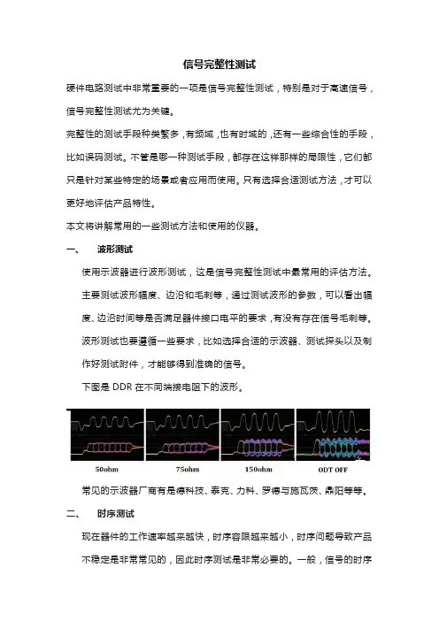
一、波形测试使用示波器进行波形测试,这是信号完整性测试中最常用的评估方法。
主要测试波形幅度、边沿和毛刺等,通过测试波形的参数,可以看出幅度、边沿时间等是否满足器件接口电平的要求,有没有存在信号毛刺等。
波形测试也要遵循一些要求,比如选择合适的示波器、测试探头以及制作好测试附件,才能够得到准确的信号。
下图是DDR在不同端接电阻下的波形。
常见的示波器厂商有是德科技、泰克、力科、罗德与施瓦茨、鼎阳等等。
二、时序测试现在器件的工作速率越来越快,时序容限越来越小,时序问题导致产品不稳定是非常常见的,因此时序测试是非常必要的。
一般,信号的时序测试是测量建立时间和保持时间,也有的时候测试不同信号网络之间的偏移,或者测量不同电源网络的上电时序。
测试时序基本都是采用的示波器测试,通常需要至少两通道的示波器和两个示波器探头(或者同轴线缆)。
下图是测量的就是保持时间:三、眼图测试眼图测试是常用的测试手段,特别是对于有规范要求的接口,比如USB、Ethernet、PCIE、HDMI和光接口等。
测试眼图的设备主要是实时示波器或者采样示波器。
一般在示波器中配合以眼图模板就可以判断设计是否满足具体总线的要求。
下图是示波器测试的一个眼图:四、抖动测试抖动测试现在越来越受到重视,常见的都是采用示波器上的软件进行抖动测试,如是德科技示波器上的EZJIT。
通过软件处理,分离出各个分量,比如总体抖动(TJ)、随机抖动(RJ)和固有抖动(DJ)以及固有抖动中的各个分量。
对于这种测试,选择的示波器,长存储和高速采样是必要条件,比如2M以上的存储器,20GSa/s的采样速率。
信号完整性常用的三种测试方法信号完整性是指在传输过程中信号能够保持原始形态和准确性的程度。
在现代高速通信和数字系统中,信号完整性测试是非常重要的工作,它能够帮助工程师评估信号的稳定性、确定系统的极限速率并发现信号失真的原因。
下面将介绍三种常用的信号完整性测试方法。
一、时域方法时域方法是信号完整性测试中最常见和最直观的方法之一、它通过观察信号在时间轴上的波形变化来评估信号的完整性。
时域方法可以检测和分析许多类型的信号失真,如峰值抖动、时钟漂移、时钟分布、幅度失真等。
时域方法的测试设备通常包括示波器和时域反射仪。
示波器可以显示信号的波形和振幅,通过观察波形的形状和幅度变化来判断信号完整性。
时域反射仪可以测量信号在传输线上的反射程度,从而评估传输线的特性阻抗和匹配度。
二、频域方法频域方法是另一种常用的信号完整性测试方法。
它通过将信号转换为频域表示,分析信号的频谱分布和频率响应来评估信号完整性。
频域方法可以检测和分析信号的频谱泄漏、频谱扩展、频率失真等。
频域方法的测试设备通常包括频谱分析仪和网络分析仪。
频谱分析仪可以显示信号的频谱图和功率谱密度,通过观察频谱的形状和峰值来评估信号完整性。
网络分析仪可以测量信号在不同频率下的响应和传输损耗,从而评估传输线的频率响应和衰减特性。
三、眼图方法眼图方法是一种特殊的信号完整性测试方法,它通过综合时域和频域信息来评估信号的完整性。
眼图是一种二维显示,用于观察信号在传输过程中的失真情况。
眼图可以提供信号的时钟抖动、峰值抖动、眼宽、眼深、眼高等指标。
眼图方法的测试设备通常包括高速数字示波器和信号发生器。
高速数字示波器可以捕捉信号的多个周期,并将其叠加在一起形成眼图。
通过观察眼图的形状和特征,工程师可以评估信号的稳定性和传输质量。
总结起来,时域方法、频域方法和眼图方法是常用的信号完整性测试方法。
它们各自具有独特的优势和适用范围,可以互相协作来全面评估信号的完整性。
在实际应用中,根据具体需求和测试对象的特点,选择合适的测试方法是非常重要的。
信号完整性测试指导书——Ver 2.0编写:黄如俭(sam Huang)钱媛(Tracy Qian)宋明全(Ivan Song)康钦山(Scott Kang)目录1. CLK Test (4)1.1 Differential Signal Test (4)1.2 Single Signal Test (7)2. LPC Test (8)2.1 EC Side Test (8)2.2 Control Sidse Test (9)3. USB Test (12)3.1 High Speed Test (12)3.2 Low Speed Test (13)3.3 Full Speed Test (13)3.4 Drop/Droop Test (14)4. VGA Test (16)4.1 R、G、B Signal Test (16)4.2 RGB Channel to Channel Skew Test (17)4.3 VSYNC and HSYNC Test (17)4.4 DDC_DATA and DDC_CKL Test (18)5. LVDS Test (19)5.1 Differential data signals swing Test (19)5.2 Checking Skew at receiver Test (20)5.3 Checking the offset voltage Test (21)5.4 Differential Input Voltage Test (23)5.5 Common Mode Voltage Test (24)5.6 Slew Rate Test (25)5.7 Data to Clock Timing Test (27)6. FSB Test (30)7. Serial Data(SATA/ESATA, PCIE, DMI,FDI)Test (33)8. HD Audio Test (35)8.1 Measurement at The Controller (35)8.2 Measurement at The Codec (36)9. DDR2 Test (39)9.1 Clock (39)9.2 Write (40)9.3 Read (42)10.Ethernet Test (44)11.SMbus Signal Test (45)12. HDMI Test (47)13. DisplayPort Test (48)1. CLK Test1.1 Differential Signal Test测试设备:示波器,两个差分探头,鼠标,键盘测试软件:3D MARK,负载测试步骤:(1)开启示波器预热30分钟,运行测试软件。

USB 2.0 Compliance Testing with Agilent Infiniium OscilloscopesApplication Note 1400Who Should Read This Application Note?Digital designers and developers working towards USB 2.0 compliance.IntroductionUniversal Serial Bus (USB) burst on the scene in 1995 delivering a revolutionary way to connect personal computers and devices. Allowing hot-plug capability, USB has introduced ease-of-use to the PC device market by providing a simple connection scheme and protocol for a wide variety of computer devices, ranging from keyboards and mice to high-bandwidth devices such as printers, scanners, and cameras.USB has now successfullyreplaced aging serial and parallel ports as the connection of choice for both device manufacturers and end users. Whereas cable length and device expansionwere limitations with older serial and parallel connections, they are no issue for USB. Amazingly,it allows devices to exist up to 30-meters away from the host, and allows up to 127 devices to be connected to a single host and port at once through a series of USB hubs. The ability to talk directly to devices or to devices through hubs allows for this incredible expansion B 1.1 worked best for slower human-interface devices such as mice and keyboards, with low-speed operating at 1.5-Mb/s and full-speed operating at12-Mb/s. Higher-bandwidth devic-es were severely limited by these relatively slow data transfer rates. As a result, the USB-Implementers Forum (USB-IF) introduced the fully backward compatible USB 2.0 in May 2000, which resulted in a 40-fold increase in datathroughput for hi-speed over full-speed. USB 2.0 operates at 480-Mb/s—ideal for devices such as video-conferencing cameras and high-resolution printers. For more information, see the official USB-IF (USB Interoperability Forum) website at .Basic SpecificationsAs listed previously, USB 2.0 comprises three different data transfer rates—low-speed,full-speed, and hi-speed.Four wires compose the cable system—V BUS, D+, D-, and ground. Devices may be either bus-powered, with 500-mA maximum bus current withdraw, or self-powered, meaning they have their own power supply.D- and D+ is a differential signal pair that serves as the primary information carrier between the host, hubs, and devices. USB 2.0 supports three different types of data transfer: interrupt, bulk, or isochronous. Control packets containing commands or query parameters may also be sent by the host.The flexibility inherent in USB is a direct result of the specifica-tions above and the stringent regulations and compliance testing mandated by the USB-IF. There are three kinds of compliance tests: framework test,interoperability test, and electri-cal test. This document onlydiscusses Infiniium’s electricaltest solution.Low, full, and hi-speed USBrequire compliance with thesignal quality, in-rush currentcheck, droop/drop and backdrive voltage electrical tests. Hi-speed requires compliance withan additional suite ofelectrical tests—hi-speed sig-nal quality, receiver sensitivity,CHIRP timing, and packetparameters. Older methods ofcompliance testing included firstcapturing the signals on a scope,then moving the data to a PC so itcould be cropped, stored in a .tsvformat, and finally analyzed inMATLAB®. The Agilent InfiniiumUSB Test Option is the first scopesolution in the industry that uti-lizes the official USB-IF MATLABscript. As the result, it providesan affordable, trustworthy, single-box, compliance solution—allow-ing you to say, as did one of ourcustomers, “I know I’m going topass!”23Full/Low-Speed Test SuiteAgilent test equipment has beenapproved by the USB-IF.Figure 1. Agilent Infiniium at official USB-IF Plugfest.The basic USB 2.0 electrical test suite includes signal quality,in-rush current check, and droop/drop tests. A SQiDD (Signal Quality inrush Droop Drop) fix-ture must be used for these tests. Agilent provides a SQiDD boardFull/Low-Speed Test Fixturethat is orderedseparately as part numberE2646A. The USB-IF exclusively uses the Agilent SQiDD board for official compliance testing.Figure 2. Agilent SQiDD board.Wire loopWire loop‘B’ Socket‘A’ Socket‘B’ Socket‘B’ Socket‘A’ Socket‘A’ SocketSwitchSwitch4Signal Quality TestUsing an oscilloscope to measure transceiver characteristics, the signal quality test looks at:• Signal eye• End of Packet (EOP) width • Signaling Rate • Rise/Fall Times• Cross-over Voltage Range • Consecutive Jitter • Paired JK Jitter • Paired KJ JitterSignal quality testing can beperformed for either upstream data or downstream data. In the case of upstream testing, signals travelling from the device to the host are captured and analyzed. Downstream testing performs just the opposite, capturing signals travelling from the host towards the device or terminating hub. Figure 3 shows a captured down-stream packet on the Infiniiumscope with the USB Test Option.Figure 3. Captured downstream packet.Signal Quality Test (continued)launched, other conditions mustalso be set in the software. Forsignal quality tests, these addi-tional conditions include tierand near end/far end. The tierrefers to the distance between thedevice and the host computer. Ifthe device is connected directly tothe host computer, the tier equals1. If the device is separated fromthe host computer by 3 hubs, thetier equals 4. Compliance testingmandates that testing occur ata minimum tier of 6; therefore,Agilent recommends that testsalways be performed with a tierFigure 4. Infiniium USB test menu.of 6. Test results may be storedin a data file on the Infiniium’sC: drive, or may also be stored toa USB flash drive.Infiniium displays all test resultsin an html format, including theeye diagram.Figure 5. Infiniium signal quality test results.5In-Rush Current Checkdictates that a surge of currentwill occur, followed by a lessersteady-state current level, whenpower is applied to a device.The hot-pluggable nature of USBrequires that the total inrushsurge current be tested to ensurethat it remains within the limitsfor the device. If the inrushcurrent does not remain withinits limits (100 mA), not only canit cause damage to the device, butit can also take power from otherdevices connected to the sameport.The USB 2.0 specification out-lines a total inrush surge currentlimit of 50-uC. A waiver is grant-ed at 150 μC.Figure 7. In-rush current spike.67Droop and Drop TestingBack-Drive Voltage TestDroop and drop testing proce-dures vary based on whether the device is self-powered or bus powered.Hosts and Self-Powered Hubs Drop testing measures the DC voltage drop across each load board attached to the SQiDD board. To get a good indication of voltage drop, the test is per-formed under two conditions—no load and load. Under no load testing, all downstream ports remain open, while the V BUS voltage test points on the SQiDD board are probed. Load testing tests the V BUS voltage test points with 500-mA loads applied to all downstream ports. The lowest measured loaded value should be used for the droop test.Droop testing involves measuring the AC voltage drop on V BUS that occurs when all but one port are under 500-mA loads; The unload-ed port is then connected to the SQiDD board. Once the instantan-cous AC voltage drop is captured on the display, markers are used to bracket the area between the lowest point and steady-state voltage point of V BUS . Infiniium then uses the bracketed data toperform the droop test.Figure 8. Droop setup for hosts and self-powered hubs.The droop test for bus-powered hubs again uses the 100-mA-load board. This load board is con-nected to all but one port on the bus-powered device. The SQiDD board is then attached to the unloaded port. Once again,markers are used to bracket the area between the lowest point on the captured data and the steady-state voltage. TheInfiniium then uses the bracketed data to run the drop test.Bus-Powered HubsDrop tests for bus-powered hubs use 100-mA load boards instead of the 500-mA load boards used in the self-powered hub proce-dure. These 100-mA boards are connected to all downstream ports. The V BUS voltage is then measured at the hub upstream port and at each downstream port. The lowest measured downstream value is used for the drop test.The back-drive voltage test is performed to ensure that a device only draws and does not sourcecurrent from V BUS on its upstream facing port at all times. If a device supplies current at this port, a number of consequences can occur, including hub enumerationfailure, PC boot failure, and motherboard failure. This test measures the DC voltages ofV BUS , D+, and D- before and after device enumeration. The voltages are then recorded on the back-drive voltage fixture. Any voltage exceeding 400-mV is considered a failure.8On the hi-speed USB Test Bed Computer, the USB hi-speedElectrical Test Tool is required.Figure 9. USB-IF hi-speed electrical test tool.Hi-Speed Electrical Test SuiteAn additional suite of tests was added to the USB 2.0 compliance procedure to accommodate the new hi-speed mode. These tests include hi-speed signal quality, receiver sensitivity, CHIRP timing, and packet parameter.Hi-Speed Electrical Test Tool9The hi-speed signal quality test utilizes the hi-speed signal quality board, as shown in Figure 10.The nomenclatures of the test points differ between the Agilent hi-speed test fixture and the Intel test fixture. The official USB test procedure is written with reference to Agilent’s test fixtures. Refer to Table 5, the cross-reference chart, whenusing Intel’s test fixture.Figure 10. Hi-speed signal quality boards (Agilent fixture andIntel fixture—device signal quality test).Hi-Speed Test Fixture10Hi-Speed Signal Quality TestInvoke the Hi-speed Electrical Test Tool software on Electrical Test bed computer and select TEST_PACKET to perform the sig-nal quality test. Figure 11 shows a hi-speed test packet captured on an Infiniium oscilloscope.Prior to testing, it must be deter-mined if the device incorporates a captive cable, or if it contains a series B or mini-B connector. During upstream tests, captive cables require that tests be run at the far end. B-connector cables require that tests be run at the near end. Figure 12 shows a hi-speed eye pattern result displayed on an Infiniiumoscilloscope.Figure 11. Hi-speed test packet.Figure 12. Hi-speed signal quality eye diagram.MonotonicityMonotonicity tests if a transmit-ted signal increases or decreases in amplitude without reversal in the opposite direction. The monotonicity characteristic of a signal can be viewed using the hi-speed signal quality eye template (Figure 12). There is no indepen-dent monotonicity test mandated by the USB-IF.Receiver SensitivityThe receiver sensitivity tests verify sensitivity of the receivers of a device on both the upstream and downstream data ports in noisy environments. The Agilent 81130A/81134A Pulse/Pattern Generator is used to emulate IN commands from the port to the device address 1. IN commands are sent from the computer to the device under test, which should be in an unsquelched mode. The noise is represented by a pre-set level, whereby a signal meeting and exceeding this level responds to the IN command with anNAK. All packets from the data generator must be NAK’d by the port under test. The amplitude of the data generator packets is then reduced in 20-mV increments as the test is run. The amplitude of these packets should be reduced until the NAK packets become infrequent. The data generator amplitude is then immediately increased to the point where the Figure 14. Receiver sensitivity test.Data generator packet Device responsegenerator packetPacket Parameters TestAnother test using the hi-speedsignal quality board tests thedevice packet parameters. Thehi-speed signal quality test boardallows for better reception of thepackets coming from the device.This test measures parameterssuch as sync field length, end ofpacket (EOP) width, and inter-packet gap.Figure 13. Device inter-packet gap.NAK packets are not intermittent. This indicates the points of minimum receiver sensitivity levels before squelch.When the device receives IN packets with a signal amplitude in excess of 150-mV, all packets should be NAK’d. When the device receives IN packetswith a signal amplitude below 100-mV, all packets should be squelched. A waiver is granted for squelch at +/- 50-mV for each level.11CHIRP Timing TestThe CHIRP test utilizes thehi-speed signal quality test fixture to measure timing and voltage on both upstream and downstream ports. The deviceis hot-plugged to the port andis immediately enumerated to capture the CHIRP handshake. Within the handshake, the CHIRP-K duration is measured to verify that it is within the 1.0-ms and 7.0-ms allowable latency. After the CHIRP K-J, K-J, K-J sequence, the device responds by turning on its hi-speed termina-tions. A drop of amplitude from800-mV nominal to 400-mV nominal occurs. The time between the beginning of thelast J in the CHIRP K-J, K-J, K-J sequence and the time whenthe device turn on initiates its hi-speed terminations must be mea-sured to verify that it is less than or equal to 500-μs.In addition to measuring thetime between the last J in CHIRP and the initiation of hi-speed termination, the CHIRPtest also measures device suspend/resume/reset timing as well as the K and J amplitudes.Figure 15. CHIRP test.Device’s chip latency(2.5 µs <-> 3 ms)Device hi-speedtermination ONFigure 16. Time between last J in CHIRP and hi-speed termination initiation.CHIRP K(1 ms <-> 7 ms)12Impedance Measurements In this test, differential time domain reflectometer (TDR) mea-surements are taken tomeasure the impedance of the hi-speed signaling path andactive terminations of the device under test. The TDR measure-ments are compared with the USB-IF specification require-ments. The device under testis powered, placed in SE0-NAK mode, and isolated from the system. D+ and D- are measuredto verify that they are 0-V ±10-mV.A 400-ps edge is then driven into the device. The resulting wave-form indicates whether or not the termination impedance and the through impedance meet the requirements. The TDR measure-ment is not required for compli-ance testing. A PASS signal quality test will suffice for the TDR measurement.Figure 17. TDR measurement.USB connectorTermination resistor1314SummaryAgilent provides a comprehen-sive, easy-to-use solution for USB compliance testing. The compli-ance testing that once took days now takes only minutes. The indi-vidualized test boards provideflexibility and affordability for the laboratory choosing to test facets of the USB specification simultaneously.In conclusion, the AgilentInfiniium USB Test Option has been described this way:“The term ‘God Send’ comes to mind. Before the arrival of this scope, a USB test was something to be avoided! It often required half a day to set up the test and an additional 30 minutes to massage the numbers into anacceptable MATLAB format.Needless to say only the minimum number of tests required was ever actually performed.“In a nutshell, this product has revolutionized the way in which we look at USB. We now have a designated test system that is reliable and easy to use and fast. The main result is that we can now provide real-time feedback, and the amount of testing we perform is probably up 30-fold or more. And as you may have guessed, the additional testing has turned up a myriad of inter-esting opportunities for future improvements. Just for fun we have even started looking at our competitor’s products!”MATLAB ® is a U.S. registered trademark of Math Works, Inc.Windows ® is a U.S. registered trademark of Microsoft Corporation.Agilent Technologies OscilloscopesMultiple form factors from 20 MHz to >90 GHz | Industry leading specs | Powerful applications15Remove all doubtOur repair and calibration services will get your equipment back to you, performing like new, when promised. You will get full value out of your Agilent equipment throughout its lifetime. Your equipment will be serviced by Agilent-trained technicians using the latest factory calibration procedures, automated repair diagnostics and genuine parts. You will always have the utmost confidence in your measurements.Agilent offers a wide range of additionalexpert test and measurement servicesfor your equipment, including initialstart-up assistance, onsite educationand training, as well as design, systemintegration, and project management.For more information on repair andcalibration services, go to:/find/removealldoubt/find/openAgilent Open simplifies the process of connecting and programming test systems to help engineers design, validate and manufacture electronic products. Agilent offers open connectivity for a broad range of system-ready instruments, open industry software, PC-standard I/O and global support, which are combined to more easily integrate test system development./find/emailupdates Get the latest information on the products and applications you select./find/agilentdirect Quickly choose and use your test equipment solutions with confidence.Agilent Email UpdatesAgilent DirectLXI is the LAN-based successor to GPIB, providing faster, more efficient connectivity. Agilent is a founding member of the LXI consortium./fi nd/usb2_compliance For more information on Agilent Technologies’ products, applications or services, please contact your local Agilent office. The complete list is available at:/fi nd/contactusAmericasCanada (877) 894-4414 Latin America 305 269 7500United States (800) 829-4444Asia Pacifi c Australia 1 800 629 485China 800 810 0189Hong Kong 800 938 693India 1 800 112 929Japan 0120 (421) 345K orea 080 769 0800Malaysia 1 800 888 848Singapore 1 800 375 8100Taiwan 0800 047 866Thailand 1 800 226 008Europe & Middle EastAustria 01 36027 71571Belgium 32 (0) 2 404 93 40 Denmark 45 70 13 15 15Finland 358 (0) 10 855 2100France 0825 010 700* *0.125 €/minute Germany 07031 464 6333****0.14 €/minuteIreland 1890 924 204Israel 972-3-9288-504/544Italy 39 02 92 60 8484Netherlands 31 (0) 20 547 2111Spain 34 (91) 631 3300Sweden 0200-88 22 55Switzerland 0800 80 53 53United Kingdom 44 (0) 118 9276201Other European Countries: /fi nd/contactusRevised: July 17, 2008Product specifi cations and descriptions in this document subject to change without notice.© Agilent Technologies, Inc. 2008Printed in USA, August 1, 20085988-6219EN。
集成电路中电源完整性与信号完整性分析哎呀,说起集成电路中的电源完整性和信号完整性分析,这可真是个让人又爱又恨的“家伙”。
就拿我之前经历的一件事儿来说吧。
有一次,我参与了一个小型电子设备的研发项目。
那时候,我们团队满心欢喜地设计好了整个集成电路的架构,觉得大功告成。
可谁知道,在实际测试的时候,问题接二连三地冒了出来。
先是电源方面,设备运行没多久,就出现了电压不稳定的情况。
这就好比你正在跑步,突然有人给你使绊子,让你的脚步变得踉踉跄跄。
我们开始仔细排查,发现是电源布线不合理,导致电流在传输过程中出现了损耗和波动。
再说说信号完整性。
明明发送出去的是清晰准确的信号,可接收端却总是出现误码和失真。
这感觉就像是你给朋友精心准备了一份礼物,结果快递给你弄破了包装,里面的东西也坏了。
那咱们先来说说电源完整性。
电源完整性简单来说,就是要确保集成电路中的电源供应稳定、干净,没有杂波和干扰。
这就像我们家里的电,如果电压一会儿高一会儿低,那电器能正常工作吗?肯定不行!在集成电路里也是一样,如果电源不稳定,那各个元器件就像失去了主心骨,没法好好干活。
比如说,在多层电路板的设计中,如果电源层和地层的间距不合理,就会产生寄生电容和电感。
这就好比在一条马路上,突然多了一些障碍物,让电流的通行变得不顺畅。
还有,电源分配网络的设计也至关重要。
如果电阻过大,电流就会遇到“堵车”,导致电压下降。
再讲讲信号完整性。
信号在集成电路中传播,就像是一场旅行。
如果路径不好,信号就会“迷路”或者“受伤”。
比如说,高速信号在传输线上传播时,如果传输线的特征阻抗不匹配,就会发生反射,这就像声音在空旷的山谷中回荡,影响了信号的质量。
还有串扰问题。
相邻的信号线就像住在隔壁的邻居,如果靠得太近,彼此之间就会互相干扰。
想象一下,你正在专心看书,旁边有人大声吵闹,你能静下心来吗?信号也是一样,被干扰了就没法准确传达信息。
为了保证电源完整性和信号完整性,我们在设计的时候要特别小心。

信号完整性验证个案分析就有关信号完整性方面的问题同大多数的电路板设计工程师们探讨,他们都会喋喋不休地说个不停,告诉你设计高速电路板是如何复杂如何危险。
他们会告诉你系统时钟超出50MHZ时,板上的信号互联会导入时序路径上的信号延时,而这些信号延时会制约板级设计的性能。
他们也会跟你描述传输线效应将如何迅速地导入类似于信号震荡、过冲和下冲这样严重的信号完整性问题,以及这些问题将如何威胁到设计的噪声容限和设计的单调一致性原理。
更有甚者信号串扰和电磁辐射的出现会严重破坏设计电路板的正常工作。
同样的问题可能得到不同的回答。
如果接触的恰恰是那些还在从事低速电路板设计的工程师,他们通常只是耸耸肩膀以示无奈。
低速电路板设计中应对潜在的信号完整性问题通常采取被动应付的传统策略,就是为设计制定合适的设计约束条件。
当一些特殊的信号通道已经出现象信号串扰或者电磁干扰这样一来严重的信号完整性问题时,通常设计工程师们总是为设计的某一部分甚至可能就是整个设计本身加入严格的物理约束。
即便这种解决方案还能满足一时之需,设计工程师也得为此付出昂贵的代价。
约束设计通常会提升最终的产品成本并且制约产品性能。
举例来说,设计工程师可能苦于找不到一个合适的位置来实现某一个特定的信号互联,而被迫增加信号板层。
然而在今天高度激烈的市场竞争中,能否做到成本最小、能否提供独到的产品性能往往意味着产品是成功还是失败。
最近一个著名的网络设备提供商的设计工程师采用Innoveda公司研发的信号完整性分析工具集XTK为他们研制的路由器产品上的一块电路板实施信号分析。
分析的结果令人震惊。
尽管该电路板工作正常,然而十分苛刻的设计规则导致实施该电路板设计需要24个电路板层,才可以避开信号完整性问题。
分析结果表明该设计严重过约束,事实上该电路板设计仅需要8个电路板层即可以加工实现,与此同时还不会介入信号完整性问题。
改进后的产品仅电路板的生产制造成本一项就节省费用高达两百万美元。
信号完整性测试规范和工作流程一、信号完整性测试规范1.测试范围:信号完整性测试应涵盖全部重要信号线,包括时钟信号、数据信号、控制信号、电源供应线等。
2.测试参数:测试参数包括但不限于信号功率、上升时间、下降时间、峰值电压、峰峰值电压、幅度稳定性、时序稳定性等。
3.测试方法:根据具体测试需求和设备条件,选择合适的信号完整性测试方法,如步进响应测试、脉冲响应测试、频率响应测试、时钟提前测试等。
4.测试设备:测试设备需要具备高精度、高速度、高带宽等特点,如示波器、信号发生器、信号注入器、信号线探针、信号整形器等。
5.测试环境:测试环境应符合实际应用场景,包括温度、湿度、电磁干扰等因素的考虑。
6.数据分析:对测试数据进行详细的分析和处理,包括波形展示、数据比对、波形参数提取、异常识别等。
7.测试标准:根据不同行业和应用领域,制定相应的信号完整性测试标准,如IEEE、IPC、JEDEC等,以确保测试结果的准确性和可靠性。
8.测试报告:根据测试结果生成详细的测试报告,包括测试方法、测试步骤、测试数据、异常情况分析、改进建议等。
二、信号完整性测试工作流程1.确定测试目标:根据设计需求和系统规格,确定需要测试的信号线和测试参数。
2.设计测试方案:根据测试目标和测试需求,设计相应的测试方案,包括测试方法、测试设备、测试环境等。
3.准备测试设备:根据测试方案,准备好所需的测试设备,确保其良好状态和准确性能。
4.连接测试回路:将被测试的电路板、电线、接插件等与测试设备连接起来,确保信号传输通畅。
5.设置测试参数:根据测试目标和测试方案,设置测试设备的相应参数,如示波器的触发电平、采样率、带宽等。
6.执行信号完整性测试:根据测试方案,执行信号完整性测试,记录测试数据和波形。
7.数据分析和处理:对测试数据进行详细分析和处理,包括波形展示、参数提取、异常识别等。
8.测试结果评估:根据测试数据和标准要求,对测试结果进行评估,确定是否合格。
信号系统功能综合测试方案综合测试联调步骤综合测试是对一个或多个子系统进行整体测试的过程,旨在验证系统在集成环境中是否能够按照预期的要求完全协同工作。
信号系统功能的综合测试方案主要包括以下步骤:1.确定测试目标:确定本次测试的目标和要求。
包括要测试的功能、性能指标、稳定性、安全性等方面。
2.梳理需求:根据系统的需求规格说明书和用户需求,将需要测试的功能点进行梳理和分类,明确每个功能点的预期结果。
3.搭建测试环境:根据系统的部署架构和配置要求,搭建符合实际情况的测试环境,包括硬件设备、操作系统、数据库等。
4.设计测试用例:根据测试目标和需求,设计相应的测试用例,包括正常场景、异常场景、边界场景等。
确保对系统的所有功能和交互进行全面覆盖。
5.编写测试脚本:将测试用例根据测试工具的要求进行编写,可以根据需要选择自动化测试还是手动测试,编写相应的脚本和测试数据。
6.执行测试用例:根据测试计划,执行测试用例。
对于自动化测试,可以通过测试工具来执行脚本;对于手动测试,测试人员需要按照预定的步骤进行测试。
7.记录测试结果:记录每个测试用例的执行结果,包括通过、失败、错误等。
对于失败和错误的用例,记录具体的错误信息和重现步骤。
8.分析和修复问题:对测试过程中发现的问题进行分析和修复。
对于功能上的问题,及时与开发人员沟通,共同找出解决方案并进行修改。
9.重复执行测试:根据修复后的版本,重新执行测试,验证修复的效果。
对于已通过的用例,可以选择部分重复执行,以加速测试过程。
10.性能和稳定性测试:在功能测试完成后,进行性能和稳定性测试,验证系统在大负载和长时间运行情况下的表现。
可以利用压力测试工具模拟大量用户并进行测试。
11.安全性测试:对于安全要求较高的信号系统,还需要进行安全性测试。
包括漏洞扫描、渗透测试等,确保系统的安全性能。
12.结果评估与报告:根据测试结果进行评估,包括功能覆盖率、问题修复率、性能指标等。
并撰写测试报告,详细记录测试过程、测试结果和问题列表。
信号完整性分析我们在滤除较为低频的噪声的时候,就应当选择电容值比较高的电容,想滤去频率较高的噪声,比如我们前面所说的EMI,则应该选择数值比较小的电容。
所以,在实际中,我们通常放置一个1uf到10uf左右的去耦电容在每个电源输出管脚处,来抑制低频成分,而选取0.01uf到0.1uf左右的去耦电容来滤除高频部分。
何为高速电路“高速电路”已经成为当今电子工程师们经常提及的一个名词,但究竟什么是高速电路?这的确是一个“熟悉”而又“模糊”的概念。
而事实上,业界对高速电路并没有一个统一的定义,通常对高速电路的界定有以下多种看法:有人认为,如果数字逻辑电路的频率达到或者超过45MHZ-50MHZ,而且工作在这个频率之上的电路已经占到了整个电子系统一定的份量(比如说1/3),就称为高速电路;也有人认为高速电路和频率并没有什么大的联系,是否高速电路只取决于它们的上升时间;还有人认为高速电路就是我们早些年没有接触过,或者说能产生并且考虑到趋肤效应的电路;更多的人则对高速进行了量化的定义,即当电路中的数字信号在传输线上的延迟大于1/2上升时间时,就叫做高速电路,本文也沿用这个定义作为考虑高速问题的标准。
此外,还有一个容易产生混淆的是“高频电路”的概念,“高频”和“高速”有什么区别呢?对于高频,很多人的理解就是较高的信号频率,虽然不能说这种看法有误,但对于高速电子设计工程师来说,理解应当更为深刻,我们除了关心信号的固有频率,还应当考虑信号发射时同时伴随产生的高阶谐波的影响,一般我们使用下面这个公式来做定义信号的发射带宽,有时也称为EMI发射带宽:F=1/(Tr*π),F是频率(GHz);Tr(纳秒)指信号的上升时间或下降时间。
通常当F>100MHz的时候,就可以称为高频电路。
所以,在数字电路中,是否是高频电路,并不在于信号频率的高低,而主要是取决于上升沿和下降沿。
根据这个公式可以推算,当上升时间小于3.185ns左右的时候,我们认为是高频电路。
信号完整性测试规范和工作流程(Ver0.9x)一.主要目的:信号完整性测试的思想是信号源输出,经过传输线到达信号末端(负载),信号本身的相对变化情况。
主要目的是验证PCB设计是否保证了信号在传输过程中能否保证其完整性,以信号的相对测试为主旨,信号本身8的绝对测试为辅。
信号比较的内容主要是信号的本征特性参数。
同时也部分验证电路原理设计的合理性。
也检验产品的性能符合国家有关标准的要求,比如3C、EMC、ESD等。
从定性参数的角度保证PCB设计达到了电路设计的要求,同时也保证产品的可靠性、一致性。
信号完整性测试一般是在线测试,因此很多测试参数在不同的工作模式下会有较大的差别。
一般情况下需要测试静态工作模式,但一些参数需要测试满负荷工作模式。
另外测试点的选择,特别是接地点的位置会对测试结果有很大的影响。
二.基本要求:要求测试准确、可靠、完善。
并要求有完整的测试报告。
这里的要求是一般通用性的要求,针对具体的产品、产品的不同阶段,可以提出不同的参数要求和具体的测试内容。
由于测试是在PCB板上(或称“在线”)的测试,因此一些测试条件和测试参数的定义条件可能会出现不一致的情况,因此规定:测试的基本状态在没有任何说明的情况下,认为是静态工作模式或额定正常工作模式。
如果在测试方法中有规定或说明的,以测试说明的条件为准。
在类型和参数中列出了比较详细全面的参数,但在测试中可能没有要求,因此,具体产品如果需要测试请加以特别说明。
一般规定:主要参数是必须测试的项目参数。
+三.类型和参数:3.1电源部分:3.1.1电源类型分为LDO电源、DC/DC电源。
3.1.2主要参数有:幅度、纹波、噪声。
3.1.3状态分为:额定负载、空载、轻载、重载、超载。
3.1.4保护能力:输出电流保护、输出电压保护、输入电压保护、热保护。
3.1.5其它参数:输入电压适应性、静态电流、关机电流(漏电流)。
3.2时钟信号:3.2.1时钟源分类:晶体时钟(正弦波时钟)、晶振时钟(方波时钟、钟振时钟)。
【信号完整性测试方法】时域测试(波形、眼图、抖动、TDR、时序)要求及仪器设备信号完整性测试方法简介信号完整性设计,在电路板设计过程中备受重视。
熟悉各类测试方法的特性,按照测试对象的特征和需求,选用合适些测试方法,对于选择方案,验证效果能够大大提高效率。
目前信号完整性的测试方法较多,从大的方向有频域测试、时域测试、其它测试。
(3类方法不是任何情况下都适合使用,信号完整性的测试方法,需要用到的仪器也很多。
)时域测试时域测试涵盖波形测试、眼图测试、抖动测试、TDR测试、时序测试。
01波形测试波形测试:是信号完整性测试最基础的方法,通常使用示波器进行测试。
测试波形的幅度、毛刺、边沿等。
通过测试波形的特征,分析幅度、边沿时间等指标是否满足要求。
波形测试需要遵循一定要求,才能保证测试误差尽量小。
⏹主机和探头一起配套的带宽要满足要求。
基板上测试系统的带宽应该在测试信号带宽的3倍以上。
在工程实践中,有的工程师随意找些探头就测试,不同厂家的探头匹配不同厂家的示波器,综合情况测试系统的误差就会很大。
⏹其次,需要注重细节。
如测试点一般选择在接收器件的附近,若条件限制无法测试,像BGA封装这类的器件,需要放在靠近Pin脚的PCB走线上或者Via上。
间隔接收器件PIn脚太远,信号发射,可能会促使测试结果和实际真实信号差异较大。
探头的接地线,也尽可能选择短的地线等。
⏹最后,应该考虑匹配。
主要关于使用同轴电缆测试的应用场景,同轴接到示波器上,负载常规是50Ω阻抗的直流耦合,对于有的电路,需要直流偏置,直接将测试系统接入会导致电路工作状态有影响,最终导致测试不到正常的波形。
02眼图测试眼图测试:针对有相关规范要求的接口(USB、SATA、HDMI、光接口)等。
通过具有MASK的示波器(含通用示波器、采样示波器、信号分析仪)。
这类示波器内部具有的时钟提取功能,能够显示眼图。
然而对于没有MASK的示波器,需要使用外接时钟实现触发。
常用信号完整性的测试手段作者:莫道春(Moore Mo)华为技术有限公司高速实验室主任信号完整性设计在产品开发中越来越受到重视,而信号完整性的测试手段种类繁多,有频域,也有时域的,还有一些综合性的手段,比如误码测试。
这些手段并非任何情况下都适合使用,都存在这样那样的局限性,合适选用,可以做到事半功倍,避免走弯路。
本文对各种测试手段进行介绍,并结合实际硬件开发活动说明如何选用,最后给出了一个测试实例。
信号完整性的测试手段很多,涉及的仪器也很多,因此熟悉各种测试手段的特点,以及根据测试对象的特性和要求,选用适当的测试手段,对于选择方案、验证效果、解决问题等硬件开发活动,都能够大大提高效率,起到事半功倍的作用。
信号完整性的测试手段信号完整性的测试手段主要可以分为三大类,如表1所示。
表中列出了大部分信号完整性测试手段,这些手段既有优点,但是也存在局限性,实际上不可能全部都使用,下面对这些手段进行一些说明。
1. 波形测试波形测试是信号完整性测试中最常用的手段,一般是使用示波器进行,主要测试波形幅度、边沿和毛刺等,通过测试波形的参数,可以看出幅度、边沿时间等是否满足器件接口电平的要求,有没有存在信号毛刺等。
由于示波器是极为通用的仪器,几乎所有的硬件工程师都会使用,但并不表示大家都使用得好。
波形测试也要遵循一些要求,才能够得到准确的信号。
首先是要求主机和探头一起组成的带宽要足够。
基本上测试系统的带宽是测试信号带宽的3倍以上就可以了。
实际使用中,有一些工程师随便找一些探头就去测试,甚至是A公司的探头插到B公司的示波器去,这种测试很难得到准确的结果。
其次要注重细节。
比如测试点通常选择放在接收器件的管脚,如果条件限制放不到上面去的,比如BGA封装的器件,可以放到最靠近管脚的PCB走线上或者过孔上面。
距离接收器件管脚过远,因为信号反射,可能会导致测试结果和实际信号差异比较大;探头的地线尽量选择短地线等。
最后,需要注意一下匹配。
USB信号完整性测试讲解USB 2.0 信号完整性测试需要使用示波器,大部分示波器使用大同小异,本文详细讲解USB2.0的信号完整性测量过程。
测试工具用于高速USB信号质量测试工具包括:1)使用SMA线缆的测试装置,如下图:该设备包括两个RF SMA (m) 垂直50 ohm 终端连接器和两个4 英寸USB A-B 电缆(E2646-61601)、一个USB 2.0 插头和USB 2.0 微型插头之间的转接插头,以及一条从主机端口给该装置供电的电缆。
下图为高速信号质量测试装置有连接SMA 电缆。
2)使用测试探头,如下图探头包括一对差分引线3)测试电缆:4)测试设备(主机)可以从USB Implementers Forum 网站的开发人员工具页下载高速电气测试工具包软件(USBHSET)。
USB设备高速信号质量测试流程操作1.在设备高速信号质量测试装置上,将TEST 开关(S1) 置于ON 位置。
验证黄色TEST LED 亮起。
2.在示波器前面板上,按下[Analyze] 分析键。
3.在"分析菜单"中,按下功能软键,选择USB 信号质量。
4.按下测试软键,选择设备高速信号质量测试。
5.按设置软键。
在"USB 信号质量"菜单中:a)按下测试连接软键,选择是使用单端(带SMA 电缆)还是差分探头连接。
b 如果使用差分连接,请按下源软键,选择连接到差分探头的模拟输入源通道。
b)如果使用单端(SMA 电缆)连接,请按下DP SMA 软键,选择连接到D+信号的模拟输入源通道。
然后,按下DN SMA 软键,选择连接到D- 信号的模拟输入源通道。
在4 通道示波器上,将强制您对D+ 和D- 信号使用不同的通道对。
这将提供最大采样率。
(通道1 和2 是一对,通道3 和4是另一对。
)通道示波器不支持使用单端SMA 电缆连接进行高速测试,因为采样率不符合所需的5 GSa/s。
c)按下测试类型软键,选择近端或远端。
信号完整性测试指导书——Ver 2.0编写:黄如俭(sam Huang)钱媛(Tracy Qian)宋明全(Ivan Song)康钦山(Scott Kang)目录1. CLK Test (3)1.1 Differential Signal Test (3)1.2 Single Signal Test (5)2. LPC Test (7)2.1 EC Side Test (7)2.2 Control Sidse Test (8)3. USB Test (11)3.1 High Speed Test (11)3.2 Low Speed Test (12)3.3 Full Speed Test (12)3.4 Drop/Droop Test (12)4. VGA Test (14)4.1 R、G、B Signal Test (14)4.2 RGB Channel to Channel Skew Test (14)4.3 VSYNC and HSYNC Test (15)4.4 DDC_DATA and DDC_CKL Test (15)5. LVDS Test (17)5.1 Differential data signals swing Test (17)5.2 Checking Skew at receiver Test (18)5.3 Checking the offset voltage Test (19)5.4 Differential Input Voltage Test (20)5.5 Common Mode Voltage Test (20)5.6 Slew Rate Test (21)5.7 Data to Clock Timing Test (23)6. FSB Test (26)7. Serial Data(SATA/ESATA, PCIE, DMI,FDI)Test (29)8. HD Audio Test (30)8.1 Measurement at The Controller (30)8.2Measurement at The Codec (31)9. DDR2 Test (34)9.1 Clock (34)9.2 Write (35)9.3 Read (37)10.Ethernet Test (39)11.SMbus Signal Test (40)12. HDMI Test (42)13. DisplayPort Test (43)1. CLK Test1.1 Differential Signal Test测试设备:示波器,两个差分探头,鼠标,键盘测试软件:3D MARK,负载测试步骤:(1)开启示波器预热30分钟,运行测试软件。
连接差分探头,鼠标,和键盘。
对示波器的probes和channals进行calibration和deskew。
(2)参照测试平台的芯片datasheet,使用Allegro SPB软件,在电路板上找出被测信号测试点,记录下过孔或芯片管脚的位置。
找出待测信号接收端的参数标准。
如图1.1图1.1(3)连接电路板的附属小板,显示屏,电源,将示波器和电路板共地。
开启电路板,正常进入系统,运行3D Mark。
(4)参照被测信号测试标准,在示波器(Agilent )的菜单选项中选择对应的测试项Frequency/Period/ Duty Cycle/High Time/ Low Time/cyc-cyc-jitter .Spec中有约束条件的要进行条件设置。
如图1.2图1.2(5)用一个差分探头连接差分信号测试点,调节示波器,抓取所需要的波形,并保存。
(6)清除之前的测试选项和波形。
再次从菜单选项中选择测试项。
Rise time/Fall time/Overshoot/Undershoot/High level/Low level(7)根据测试标准的要求,选择相应的探头。
如果要求使用单端探头,将探头的“+”端接信号测试点,“-”端接地;如果要求使用差分探头,将探头连接差分信号的两个测试点,调节示波器,抓取所需要的波形,并保存。
(8)Vcross的测试:a.用两个单端探头的“+”极分别连接clk信号的P/N极,“—”极连接差分信号测试点最近的地。
在同一屏幕上显示两个通道的波形,调整参数使两个通道的OFFSET,单位幅值相同,抓取密集波形。
调出marker,用两条横向的坐标分别卡出两条信号线交点(同一信号相同的边沿)的最大值和最小值。
如图1.3图1.3b.使用无限累积功能,抓取一个交点的累积波形。
调出Marker,用两条横向坐标轴分别卡出交点的最大值和最小值。
两条横项坐标轴的值就是V_cross的值。
如图1.4图1.4(9)Vcross detal的测试:依照Vcross的测试方法,测出Vcross的最大值和最小值,两值的差(即两条Marker值差的绝对值)就是Vcross detal.测试标准:将测得的数据与测试标准对照,判断测试结果是否在标准之内。
若在,则测试结果合格,定为PASS。
若不在标准之内,则测试结果不合格,定为FAIL。
注意事项:(1)测试时,要将示波器与电路板共地。
(2)测试Rise time/Fall time/Overshoot/Undershoot/ High level/Low level时,依据给定的标准选择使用差分探头或时单端探头。
(3)对于测试标准中有约束条件的测试项,要按照标准更改示波器的条件设置,测得的数据才可与标准值比对。
比如,对高电平和低电平范围的规定。
(4)信号的测试标准参考接收芯片端 datasheet 的数据。
1.2 Single Signal Test测试设备:示波器,两个单端探头,鼠标,键盘测试软件:3D MARK,负载测试步骤:(1)-(3)同差分信号测试。
(4)参照信号在接收芯片端的测试标准,从示波器测试软件的菜单选项中选择测试项。
Spec中有约束条件的要进行条件设置。
Frequency/Period/High Time/Low Time/Rise time/Fall time/Overshoot/Undershoot/ Duty Cycle/ Cycle to cycle Jitter/High level/Low level(5)用单端探头探接测试点,调节示波器旋钮,抓取所需要的波形,并保存。
测试标准:将测得的数据与测试标准对照,判断测试结果是否在标准之内。
若在,则测试结果合格,定为PASS。
若不在标准之内,则测试结果不合格,定为FAIL。
注意事项:(1)对于测试标准中有约束条件的测试项,要按照标准更改示波器的条件设置,测得的数据才可与标准值比对。
比如,对高电平和低电平范围的规定。
(2)信号的测试标准参考接收芯片端 datasheet 的数据。
2. LPC Test2.1 EC Side Test测试设备:示波器,两个单端探头,鼠标,键盘测试步骤:(1)开启示波器预热30分钟,运行测试软件。
连接单端探头,鼠标,和键盘。
对示波器的probes和channals进行calibration和deskew。
(2)参照电路图,使用Allegro SPB软件,找出线路最长和最短的LPC数据信号LPC_AD,记录下待测信号的位置。
找出待测信号在EC芯片端的参数标准。
如图2.1。
图2.1 at receiver of EC(3)连接电路板的LCD和电源,将示波器和电路板共地。
开启电路板,正常进入系统.(4)用两个单端探头分别连接LPC_CLK信号和LPC_AD信号在EC芯片端的测试点,调节示波器旋钮,待设置完成后,重新启动计算机以抓取波形。
(5)调出Marker其mark point按照SPEC来定义,测出所需参数值。
如图2.2图2.2 at receiver of EC2.2 Control Sidse Test测试设备:示波器,两个单端探头,鼠标,键盘测试步骤:(1)开启示波器预热30分钟,运行测试软件。
连接单端探头,鼠标,和键盘。
对示波器的probes和channals进行calibration和deskew。
(2)参照芯片的datasheet,使用Allegro SPB软件,找出线路最长和最短的LPC数据信号LPC_AD,记录下待测信号的位置。
找出待测信号在Control端的参数标准。
如图2.3。
图2.3 at receiver of ISCH(3)连接电路的LCD和电源,将示波器和电路板共地。
开启电路板,正常进入系统.(4)用两个单端探头分别连接LPC_CLOUT信号测试点和LPC_AD信号测试点,调节示波器旋钮,待设置完成后,重新启动计算机以抓取波形。
(5)调出Marker其mark point按照SPEC来定义,测出所需参数值.如图2.4图2.4 at receiver of ISCH测试标准:将测得的数据与测试标准对照,判断测试结果是否在标准之内。
若在,则测试结果合格,定为PASS。
若不在标准之内,则测试结果不合格,定为FAIL。
注意事项:(1)对于测试标准中有约束条件的测试项,要按照标准更改示波器的条件设置,测得的数据才可与标准值比对。
比如测量波形的数据时,Test point 要根据datasheet设定。
(2)信号的测试标准参考接收芯片端芯片 datasheet 的数据。
3. USB Test3.1 High Speed Test测试设备:示波器(MSO90404A),1168A,E2678A,E2649(USB测试夹具),USB Cable(若干)。
测试软件:USB一致性测试软件,USBHSET software。
测试步骤:(1)打开示波器,预热30分钟左右。
(2)运行一致性测试软件,进入软件Set Up设置页面,将Device Test Point设置为Host,Test Method设置为Matlab。
图3.1(3)Select Tests设置,选择High Speed Test。
(4)Configure设置,选择测试通道,特征参数为High Speed Near End。
(5)按照Connect测试界面提示的连接方法,选择相应的测试夹具,进行连接。
(6)确认连接无误后,运行测试。
(7)查看测试报告,保存测试报告。
3.2 Low Speed Test测试设备:示波器(MSO90404A),2*N2873A,E2649(USB测试夹具),Low Speed Device,USB Cable(若干)。
测试软件:USB一致性测试软件测试步骤:(1)运行一致性测试软件,进入软件Set Up设置页面,将Device Test Point设置为Host,Test Method设置为Matlab。